Table of Contents
Advertisement
Specifications
n AMPLIFIER SECTION
RMS output power
THD 10%, both channels driven
1 kHz
(Low channel)
10 kHz
(High channel)
80 Hz
(Subwoofer channel)
Total power output
PMPO
FTC output power
THD 10%, both channels driven
100 Hz-3 kHz
(Low channel)
3 kHz-10 kHz
(High channel)
50 Hz-100 Hz
(Subwoofer channel)
Total FTC power
n FM/AM TUNER, TERMINALS SECTION
Preset station
Frequency Modulation (FM)
Frequency range
75 W per channel (5 Ω)
70 W per channel (5 Ω)
160 W (8 Ω)
450 W
4000 W
59 W per channel (5 Ω)
57 W per channel (5 Ω)
130 W (8 Ω)
362 W
FM 15 stations
AM 15 stations
87.9 - 107.9 MHz (200 kHz steps)
87.5 - 108.0 MHz (100 kHz steps)
SA-AK631PL
Colour
(S)... Silver Type
Sensitivity
S/N 26 dB
Antenna terminal(s)
Amplitude Modulation (AM)
Frequency range
Sensitivity
S/N 20 dB (at 1000 kHz)
Audio performance (Amplifier)
Input sensitivity/Input impedance
Aux
Phone jack
Terminal
Mic jack
Terminal
n CASSETTE DECK SECTION
Track system
Heads
Record/playback
Erasure
Motor
Recording system
Erasing system
Tape speed
Overall frequency response (+3 dB, -6 dB at DECK OUT)
NORMAL
S/N ratio
© 2004 Matsushita Electric Industrial Co. Ltd.. All
rights
reserved.
distribution is a violation of law.
ORDER NO. MD0412590C3
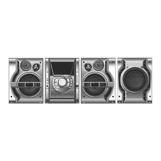
CD Stereo System
2.5 µV (IHF)
75 Ω (unbalanced)
520 - 1710 kHz (10 kHz steps)
250 mV,14.7 kΩ
Stereo, 3.5 mm jack
0.7mV, 680 Ω
Mono, 3.5 mm
4 track, 2 channel
Solid permalloy head
Double gap ferrite head
DC servo motor
AC bias 100 kHz
AC erase 100 kHz
35 Hz - 14 kHz
50 dB (A weighted)
Unauthorized
copying
2.2 µV
560 µV/m
4.8 cm/s
and
Advertisement
Table of Contents

Related Manuals for Panasonic SA-AK631PL


Summary of Contents for Panasonic SA-AK631PL
-
Page 1: Specifications
ORDER NO. MD0412590C3 CD Stereo System SA-AK631PL Colour (S)... Silver Type Specifications n AMPLIFIER SECTION Sensitivity 2.5 µV (IHF) RMS output power S/N 26 dB 2.2 µV THD 10%, both channels driven Antenna terminal(s) 75 Ω (unbalanced) 1 kHz Amplitude Modulation (AM) 75 W per channel (5 Ω) -
Page 2: Table Of Contents
SA-AK63 1PL Wow and flutter 0.18 % (WRMS) Audio output (Disc) Fast forward and rewind time Approx. 120 seconds with Number of channels 2 (Stereo) (FL,FR) C-60 cassette tape n GENERAL n DISC SECTION Power Supply AC 120 V, 60Hz Discs played [8 cm or 12 cm] Power consumption 255 W... - Page 3 SA-AK63 1PL 12.4. Micon ROM Checksum and Version Display Mode 17.4. (D) Transformer P.C.B. 13 Measurements and Adjustments 17.5. (E) CD Detect P.C.B., (F) Spindle Position P.C.B., (G) CD 13.1. Cassette Deck Section Loading P.C.B. & (K) Tuner Pack P.C.B. 13.2.
-
Page 4: Before Repair And Adjustment
SA-AK63 1PL 1 Before Repair and Adjustment Disconnect AC power, discharge Power Supply Capacitors C5820 and C5840 through a 10Ω, 5W resistor to ground. DO NOT SHORT-CIRCUIT DIRECTLY (with a screwdriver blade, for instance), as this may destroy solid state devices. After repairs are completed, restore power gradually using a variac, to avoid overcurrent. -
Page 5: Prevention Of Electro Static Discharge (Esd) To Electrostatically Sensitive (Es) Devices
SA-AK63 1PL 3 Prevention of Electro Static Discharge (ESD) to Electrostatically Sensitive (ES) Devices Some semiconductor (solid state) devices can be damaged easily by electricity. Such components commonly are called Electrostatica lly Sensitive (ES) Devices. Examples of typical ES devices are integrated circuits and some field- effect transistors and semiconductor “chip”... -
Page 6: Handling Precautions For Traverse Deck
SA-AK63 1PL 5 Handling Precautions For Traverse Deck The laser diode in the traverse deck (optical pickup) may break down due to potential difference caused by static electricity of clothes or human body. So, be careful of electrostatic breakdown during repair of the traverse deck (optical pickup). ·... -
Page 7: Precaution Of Laser Diode
SA-AK63 1PL 6 Precaution of Laser Diode CAUTION: This unit utilizes a class 1 laser. Invisible laser radiation is emitted from the optical pickup lens. Wavelength: 780nm When the unit is turned on: 1. Do not look directly into the pick up lens. 2. -
Page 8: Accessories
SA-AK63 1PL 7 Accessories Remote Control FM Antenna AC Cord AM Loop Antenna... -
Page 9: Operation Procedures
SA-AK63 1PL 8 Operation Procedures... - Page 10 SA-AK63 1PL...
-
Page 11: Disassembly And Assembly Of Main Component
SA-AK63 1PL 9 Disassembly and Assembly of Main Component “ATTENTION SERVICER” Some chassis components may have sharp edges. Be careful when disassemblin g and servicing. 1. This section describes procedures for checking the operation of the major printed circuit boards and replacing the main components. -
Page 12: Gear For Servicing (Jig) Information
SA-AK63 1PL 9.2. Gear for servicing (jig) Information 1. This unit has a gear which is used for checking items (Open/Close of disc tray, up/down operation of traverse unit by manually) when servicing. 2. For preparation of gear (for servicing), perform the procedures as follows. 3. -
Page 13: Disassembly Of Top Cabinet
SA-AK63 1PL 9.3. Disassembly of Top Cabinet Step 1 Remove 2 screws at each side and 5 screws at rear panel. Step 2 Lift up both sides of the top cabinet, push the top cabinet towards the rear and remove the top cabinet. 9.4. - Page 14 SA-AK63 1PL Step 2 Release the 2 claws, and then remove the CD lid cover. Step 6 Press the POWER button to turn the power off. · [Opening the disc tray manually (Using service tools)] Step 3 Repeat Step 2 but rotate the gear tools in anti-clockwise direction.
-
Page 15: Disassembly Of Rear Panel
SA-AK63 1PL 9.5. Disassembly of Rear Panel · Follow the (Step 1) - (Step 2) of Item 9.3 - Disassembly of Top Cabinet Step 1 Remove 7 screws and disconnect wire CN2810 (Fan) at rear cabinet as shown. 9.6. Disassembly of CD Mechanism Unit ·... -
Page 16: Disassembly Of Main P.c.b
SA-AK63 1PL 9.7. Disassembly of Main P.C.B. · Follow the (Step 1) - (Step 2) of Item 9.3 - Disassembly of Top Cabinet · Follow the (Step 1) - (Step 6) of Item 9.4 - Disassembly of CD Lid · Follow the (Step 1) of Item 9.5 - Disassembly of Rear Panel ·... -
Page 17: Disassembly Of Power P.c.b
SA-AK63 1PL · Replacement of Power Amplifier IC Step 1 Desolder the terminals of Power Amplifier IC and replace the component. 9.9. Disassembly of Power P.C.B. · Follow the (Step 1) - (Step 2) of Item 9.3 - Disassembly of Top Cabinet ·... -
Page 18: Disassembly Of Transformer P.c.b
SA-AK63 1PL · Replacement of the Power Amplifier IC/ Voltage Regulator Step 3 Unsolder the terminals of Power Amp IC, transistor and replace the components. Step 4 Fix back the cut portion with a screw as shown. Step 1 Remove 2 screws fixed to the Power Amplifier IC and 1 screw to Voltage Regulator. -
Page 19: Disassembly Of Front Panel Unit
SA-AK63 1PL 9.11. Disassembly of Front Panel Unit · Follow the (Step 1) - (Step 2) of Item 9.3 - Disassembly of Top Cabinet · Follow the (Step 1) - (Step 6) of Item 9.4 - Disassembly of CD Lid ·... -
Page 20: Cd Mechanism Main Component Replacement Procedures
SA-AK63 1PL Step 5 Tilt the cassette mechanism unit in the direction of arrow (1), and then remove it in the direction of arrow (2). · For replacement of Deck Mechanism P.C.B. Step 6 Remove 3 screws. Step 7 Unsolder the motor terminals. Step 8 Remove Deck Mechanism P.C.B. - Page 21 SA-AK63 1PL Caution: When removing or inserting the traverse deck avoid touching the OPU lens and pressing onto the turntable. Step 8 Remove 3 screws. Step 9 Unsolder the motor terminals (4 points). Step 4 With pressing the claw (A), rotate the hexagonal wrench clockwise.
- Page 22 SA-AK63 1PL Step 11 Remove the pin. · Note for installation of the CD servo P.C.B. Step 12 Release the claw, and then remove the traverse deck ass’y. Note: · Installation for traverse deck ass’y Be careful not to lose the 3 floating spring because those will also be removed on removal of the traverse deck ass’y.
- Page 23 SA-AK63 1PL Step 4 Force the disc tray fully. Step 3 Force the claw of timing lever. Step 5 With pressing the claw (B) in the direction of arrow (1), force the connection lever in the direction of arrow (2). 9.13.2.
- Page 24 SA-AK63 1PL Step 6 Insert the gear with hexagonal wrench into the hole. Step 9 With forcing the left guide bar manually because the left guide bar interfers with claw, draw the disc tray. [Installation of the disc tray after replacement] Step 7 Rotate the hexagonal wrench in the direction of arrow, and then open the disc tray fully.
- Page 25 SA-AK63 1PL NOTE: Force the right guide bar of tray base manually not to move upwards. Step 4 Holding the disc tray manually, push the disc tray in the direction of the arrow. 9.13.3. Disassembly and reassembly for mechanism base drive unit Step 1 Remove 3 screws.
- Page 26 SA-AK63 1PL Step 9 Pressing the claw (B) in the direction of arrow (1), force the connection lever in the direction of arrow (2). Step 6 Install the tray lock spring to hook temporary. Step 7 Release the claw, and then remove the tray lock. Step 8 Release the claw, and then remove the rear lock.
- Page 27 SA-AK63 1PL Step 13 Remove the traverse relay gear, traverse cam gear and drive gear. Step 11 Lift up the left end of spindle base unit in the direction of arrow (1), and then remove the unit in the direction of arrow (2).
- Page 28 SA-AK63 1PL Step 3 Rotate the disc lever in the direction of arrow (1), draw the disc lever. NOTE: Hold the loading stopper ass’y manually bacause it is flipped by spring. NOTE: Take care not to lose the disc lever spring. Step 6 Remove the cushion spring.
- Page 29 SA-AK63 1PL Step 8 Release the 2 claws, and then remove the relay gear A. Step 9 Release the 2 claws, and then remove the spindle shaft. Step 12 Squeeze the shaft of lower hook, and then draw it. Step 13 Rotate the lower spindle in the direction of arrow until Step 10 Remove the lower spindle spring with tweezers.
- Page 30 SA-AK63 1PL spread the hold bars of loading stopper and remove the Step 1 Install the traverse cam gear. UP/DOWN base. Step 2 Rotate the traverse cam gear to the direction of arrow. [Installation for loading stopper ass’y] Step 1 Align the claw of loading stoppers ass’y with the slot of spindle base.
- Page 31 SA-AK63 1PL Step 4 Install the slide plate 2 to the mechanism base, and then match to the connection lever. Step 7 Move the slide plate 1 to forward fully. Step 5 Install the slide plate 1 to the mechanism base, and then match to the connection leve and align the trapezoid tooth Step 8 Install the rear lock.
- Page 32 SA-AK63 1PL Step 13 Install the gear holder, and then tighten the screw (a). Step 11 Remove the tray lock spring from hook,and then latch to the tray lock. Step 12 Install the UP/DOWN gear, change gear, change gear spring, pulley gear and belt in the order of (1) - (5). Step 14 Install the tray base, traverse ass’y, mechanism cover and upper plate.
- Page 33 SA-AK63 1PL 9.13.4. Replacement for the motor ass’y P.C.B. Step 7 Release the claw (B), and then remove the motor ass’y. [Notice for motor ass’y installation] 1. Locate the name plate of motor to the traverse ass’y. 2. Align the hole of motor with the ribs. Step 1 Install the belt temporarily.
- Page 34 SA-AK63 1PL 9.14. Replacement for the pinch roller ass’y and head block · Follow the (Step 1) - (Step 2) of Item 9.3 - Disassembly of Top Cabinet · Follow the (Step 1) - (Step 6) of Item 9.4 - Disassembly of CD Lid ·...
-
Page 35: Replacement For The Deck Motor Ass
SA-AK63 1PL 9.15. Replacement for the Deck motor ass’y, capstan belt A, capstan belt B and winding belt · Follow the (Step 1) - (Step 2) of Item 9.3 - Disassembly of Top Cabinet · Follow the (Step 1) - (Step 6) of Item 9.4 - Disassembly of CD Lid ·... - Page 36 SA-AK63 1PL Step 7 Put the capstan belt A temporarily as shown below. Step 2 Put the winding belt on the pulley temporarily. Step 3 Install the flywheel F. Step 4 Put the winding belt on the flywheel F. Step 5 Install the winding lever and spring while pressing the winding arm in the direction of arrow.
- Page 37 SA-AK63 1PL Step 10 Remove 3 screws. Step 11 Put the capstan belt B as shown below. Step 12 Put the capstan belt A on the motor ass’y pulley.
-
Page 38: Replacement For The Cassette Lid Ass
SA-AK63 1PL 9.16. Replacement for the cassette lid ass’y · Follow the (Step 1) - (Step 2) of Item 9.3 - Disassembly of Top Cabinet Step 1 Lift up the lever upward, open the cassette lid ass’y. (For DECK1 and DECK2) Step 2 Push up the cassette lid ass’y in the direction of arrow. -
Page 39: Rectification For Tape Jam Problem
SA-AK63 1PL 9.17. Rectification for tape jam problem · Follow the (Step 1) - (Step 2) of Item 9.3 - Disassembly of Top Cabinet Step 1 If a cassette tape cannot be removed from the deck (the tape is caught by the capstan or pinch roller during playback or recording), rotate the flywheel F in the direction of the arrow to remove it. -
Page 40: Checking For Major P.c.bs
SA-AK63 1PL 10 Checking for major P.C.Bs Note: Checking of all major P.C.Bs (Main P.C.B., Panel P.C.B., Transformer P.C.B., Deck P.C.B., Deck Mechanism P.C.B., Sub- Power P.C.B. and Power P.C.B.) can be carried out using below procedures. For the disassemblin g procedures, refer to Section 9. 10.1. -
Page 41: Checking Of Transformer P.c.b
SA-AK63 1PL 10.2. Checking of Transformer P.C.B. 1. Remove Top Cabinet and Rear Panel. 2. Remove CD Lid. 3. Disassemble CD Mechanism Unit. 4. Connect FFC wires (CN2801 & CN2805) from CD Mechanism Unit. -
Page 42: Checking Of Panel, Deck & Deck Mechanism P.c.b
SA-AK63 1PL 10.3. Checking of Panel, Deck & Deck Mechanism P.C.B. 1. Remove Top Cabinet. 2. Remove CD Lid. 3. Disassemble CD Mechanism Unit. 4. Remove volume knob at Front Panel Unit. 5. Disassemble Panel P.C.B. 6. Disassemble Deck Mechanism Unit. 7. -
Page 43: Checking Of Power P.c.b
SA-AK63 1PL 10.4. Checking of Power P.C.B. 1. Remove Top Cabinet and Rear Panel. 2. Remove CD Lid. 3. Disassemble CD Mechanism Unit. 4. Remove 3 screws at Transformer P.C.B.. 5. Remove 2 screws at heat sink and 1 screw at Power P.C.B. 6. -
Page 44: Self-Diagnostic Function
SA-AK63 1PL 11 Self-Diagnostic Function 11.1. Self-diagnostic display This unit is equipped with a self-diagnost ic display function which, will display an error code corresponding to the problem occuring. Use this function when performing checking maintenance on the unit. 11.2. How to enter the Self-Diagnostic Function 11.3. -
Page 45: To Clear All Error Code
SA-AK63 1PL 3. Press to close the tray. 4. Press “CD DIRECT PLAY (5)” and wait until the tray is open. 5. Press and remove the CD. 6. Press to close the tray. 7. Press “n/STOP” to indicate Error Code. ·... - Page 46 SA-AK63 1PL 11.8.3. Power supply related error detection Abnormal Items Error Display Method of Detection POWER AMP output abnormal During normal operation, if DCDET becomes ‘L’, normal POWER OFF process shall not be executed, PCNT shall be switched to ‘L’ immediately.
-
Page 47: Cd Test Mode Function
SA-AK63 1PL 12 CD Test Mode Function This CD test mode is provided to check CD unit without connecting to changer loading mechanism. This mode shall operate CD PLAY with CD unit being connected only and CD Automatic Alignment result is shown on FL display. 12.1. -
Page 48: Micon Rom Checksum And Version Display Mode
SA-AK63 1PL · It shall move up one counter when the above operations ends. The counter will reset to 00000 when 99999 is reached. · To exit CD aging test mode, press button, the tray will return to its PLAY position and power will be off. 12.4. -
Page 49: Measurements And Adjustments
SA-AK63 1PL 13 Measurements and Adjustments 13.1. Cassette Deck Section standard value. Bias voltage for Deck 2 14±4mV (Normal) · Measurement Condition Erase voltage for Deck 2 80mV (Normal) − − − − Make sure head, capstan and press roller are clean. −... -
Page 50: Alignment Points
SA-AK63 1PL 9. Set AM-SG to 520kHz. 10. Receive 520kHz in the unit. 11. Adjust L2602 (OSC) so that the EVM-DC value is with 1.1±0.5V. Fig.6 13.2.2. AM RF Adjustment 1. Connect the instrument as shown in Fig. 7. 2. Set the unit to AM mode. 3. -
Page 51: Block Diagram
SA-AK63 1PL 14 Block Diagram OPTICAL PICKUP SEMICONDUCTOR LASER Q7601 LASER POWER DRIVE PHOTO DETECTOR IC7003 AN8739SBTE2 FOCUS COIL/TRACKING COIL/ TRAVERSE MOTOR/ SPINDLE MOTOR DRIVE /RST RESET SIGNAL GENERATOR FOCUS FOCUS COIL COIL DRIVE TRACKING COIL TRACKING COIL DRIVE TRAVERSE M7301 TRVP MOTOR... - Page 52 SA-AK63 1PL TO MAIN BLOCK X7201 NTEST IOMODE CD_RST NRST TXTCK MICRO COMPUTER TIMING GENERATOR DSL/PLL/VCO INTERFACE TXTD DQSY RFVDD (SBCK) EFM DEMODULATION SUBCODE (SUBC) VREF SPINDLE SYNC INTERPOLATION INTERFACE SERVO CIRC ECC (TXNCLDCK) CDROM ECC A, B, C, D, E, F 30~35 A,B,C,D,E,F FLAG...
- Page 53 SA-AK63 1PL AM ANT FM ANT Z2620 CF2601 CF2602 Q1 (RF AMP) Q2601 MIXER IF AMP D2602 L2602 L2601 BUFFER (FM) DECODER RM AMP BUFFER PHASE PILOT CANCEL STEREO LEVEL S-CURVE SWITCH AM/FM COMP BUFFER TUNING DRIVE PILOT IC2601 X2602 LA1833NMNTLM Z2602 FM/AM IF AMP,...
- Page 54 SA-AK63 1PL FL6601 FROM POWER FL DISPLAY TRANSFORMER 50~84 7~14, 30~37 16~23, 1~4, 25~51 53~64 IC6601 C0HBB0000039 FL DRIVER C0GAM0000005 MOTOR DRIVE OUT1 OUT2 POWER SUPPLY CONTROL PLLDA Q2907 STAT SWITCH PUSH Q2936 CD MOTOR PUSH SUPPLY ST/DO SWITCH OPEN PLLCLK Q2906 BLKCK...
- Page 55 SA-AK63 1PL IC1001 AN7348S-E1 P.B EQ/REC AMP/ ALC/TPS AMP 24(23) (DECK 1) P.B. HEAD 1(2) 20(5) 22(3) 21(4) 17(8) (DECK 2) R/P HEAD 18(7) LOGIC L/H NOR/CrO & HI/LO LOGIC RIPPLE LOGIC REJECTION REC/PB Q6501, Q6502 JK6501 Q2978 SWITCH (DECK 2) ERASE HEAD L1002 BIAS OSC...
- Page 56 SA-AK63 1PL IC2804 7(8) B1(2) C0AABA000009 DUAL OP-AMP Q2181 (Q2281) 22(21) 2(6) 13(14) OUT1(2) JK2801 HPF FREQ E1(2) 1(7) FILTER 3(5) SWITCH Q2142 (Q2242) 9(10) CD SIGNAL C1(2) CONTROL IC2806 C0ABBB000244 DUAL OP-AMP 5(6) IC2803 A1(2) C1BB00000732 AUDIO SOUND PROCESSOR 32(31) REC1(2) HP_L(R)
- Page 57 SA-AK63 1PL IC2810 C0ABBB000244 DUAL OP-AMP SUBW FILTER Q2553 Q2551 SUBWOOFER SW_LV1 LEVEL SWITCH CONTROL DC_DET Q2554 Q2552 SUBWOOFER SW_LV2 LEVEL SWITCH CONTROL HP_SW SYNC MUTE_H...
- Page 58 SA-AK63 1PL 16(15) 3(6) -IN2 1(2) OUT 2 1(2) HIGH CH (6 W) IC5801 JK5851 (JK5852) RSN315H42C-P POWER HIC 7(9) 13(12) -IN1 1(2) OUT 1 1(2) LOW CH (6 W) 4(2) +VCC 1(2) FILTER 5(1) -VCC 1(2) 4(1) 10(14) D5814 IN GND AC DET AC DET...
-
Page 59: Voltage Measurement
SA-AK63 1PL 15 Voltage Measurement... - Page 60 SA-AK63 1PL...
-
Page 61: Schematic Diagram
SA-AK63 1PL 16 Schematic Diagram (All schematic diagrams may be modified at any time with the Caution ! development of the new technology) IC, LSI and VLSI are sensitive to static electricity. Note: Secondary trouble can be prevented by taking care during : Push switch repair. -
Page 62: A) Cd Servo Circuit
SA-AK63 1PL 16.1. (A) CD Servo Circuit SCHEMATIC DIAGRAM - 1 : +B SIGNAL LINE : CD-DA SIGNAL LINE OPTICAL PICKUP CIRCUIT CD SERVO CIRCUIT Q7601 LASER DIODE B1ADCF000001 R7601 C7601 C7670 C7204 C7203 LASER POWER DRIVE 6.3V33 6.3V220 Q7601 R7650 LD GND NBOUT... - Page 63 SA-AK63 1PL SCHEMATIC DIAGRAM - 2 : +B SIGNAL LINE : CD SIGNAL LINE : CD-DA SIGNAL LINE CD SERVO CIRCUIT C7626 C7625 C7224 C7223 6.3V220 6.3V100 R7217 C7225 1000P C7226 R7211 1000P R7218 R7221 C7231 C7230 6.3V220 R7212 C7234 C7233 C7232 16V10...
-
Page 64: B) Main (Tuner) Circuit
SA-AK63 1PL 16.2. (B) Main (Tuner) Circuit SCHEMATIC DIAGRAM - 3 : +B SIGNAL LINE : FM SIGNAL LINE : AM SIGNAL LINE : FM/AM SIGNAL LINE : FM OSC SIGNAL LINE : AM OSC SIGNAL LINE MAIN (TUNER) CIRCUIT R2604 Q2606 TUNER PACK CIRCUIT... -
Page 65: B) Main Circuit
SA-AK63 1PL 16.3. (B) Main Circuit SCHEMATIC DIAGRAM - 4 : PLAYBACK SIGNAL LINE : AUX SIGNAL LINE : +B SIGNAL LINE : -B SIGNAL LINE : RECORD SIGNAL LINE : MAIN SIGNAL LINE MAIN CIRCUIT Q2980 Q2978 B1GDCFJJ0023 B1GDCFJJ0023 DECK MOTOR SWITCH CR02 SWITCH... -
Page 66: Main Circuit
SA-AK63 1PL SCHEMATIC DIAGRAM - 5 : CD SIGNAL LINE : +B SIGNAL LINE PANEL CIRCUIT : -B SIGNAL LINE (CN6601) ON : MAIN SIGNAL LINE SCHEMATIC DIAGRAM-10 MAIN CIRCUIT CN2806 36 35 34 33 32 31 30 29 28 27 26 25 15 14 13 12 11 10 R2006 C2752... - Page 67 SA-AK63 1PL SCHEMATIC DIAGRAM - 6 : -B SIGNAL LINE : +B SIGNAL LINE TO FAN UNIT MAIN CIRCUIT CN2810 R2595 R2414 R2420 R2591 R2338 D2332 330K C2415 B0ADCC000002 R2415 R2413 R2337 C2334 R2333 C2332 470K 0.22 R2331 R2419 R2412 5.6K C2414 C2413...
- Page 68 SA-AK63 1PL SCHEMATIC DIAGRAM - 7 : +B SIGNAL LINE MAIN CIRCUIT VREF+ R2827 R2830 64 63 MCLK MCLK RESTSW /RESTSW CHG_HLF CHG_HLF R2834 DCDET CHG_CW CHG_CW DCDET CHG_CCW PCONT CHG_CCW PCONT/EFP_/CE CHG_SW1 CHG_SW1 CHG_SW2 CHG_SW2 CHG_PLR EE_DAT CHG_PLR EE_DAT EE_CLK CHG_AD2 R2856...
- Page 69 SA-AK63 1PL SCHEMATIC DIAGRAM - 8 : +B SIGNAL LINE : AUX SIGNAL LINE : MAIN SIGNAL LINE : -B SIGNAL LINE : CD SIGNAL LINE : PLAYBACK SIGNAL LINE : RECORD SIGNAL LINE : FM/AM SIGNAL LINE MAIN CIRCUIT D2951 B0BC7R500001 C2952...
-
Page 70: C) Panel Circuit
SA-AK63 1PL 16.4. (C) Panel Circuit SCHEMATIC DIAGRAM - 9 : +B SIGNAL LINE : MAIN SIGNAL LINE : -B SIGNAL LINE PANEL CIRCUIT SYS6V S6210 S6310 R6458 DECK1 ENTER 4.7K OPEN R6310 D6458 S6209 B3AAA00000583 S6309 POWER KEY3 TITLE SEARCH R6309 S6301... -
Page 71: Panel Circuit
SA-AK63 1PL SCHEMATIC DIAGRAM - 10 : +B SIGNAL LINE : -B SIGNAL LINE : MAIN SIGNAL LINE PANEL CIRCUIT MICSW L6502 R6506 C6505 R6503 2.2K C6510 0.047 50V1 R6501 R6509 C6509 C6506 C6501 0.01 C6503 0.01 50V1 C6504 0.047 L6501 R6505 330K... -
Page 72: D) Transformer Circuit
SA-AK63 1PL 16.5. (D) Transformer Circuit SCHEMATIC DIAGRAM - 11 : +B SIGNAL LINE : -B SIGNAL LINE TRANSFORMER CIRCUIT D5950-D5953, D5970-D5973 B0EAMM000038 VCC+ D5952 D5950 VCC- D5972 C5960 D5970 POWER D5973 D5971 CIRCUIT AC GND D5953 (H5950/ D5951 T5950 W5950) ON G4C7AFD00014 R5965... - Page 73 SA-AK63 1PL 16.6. (E) CD Detect Circuit, (F) Spindle Position Circuit, (G) CD Loading Circuit & (L) Sub-Power Circuit SCHEMATIC DIAGRAM - 12 : +B SIGNAL LINE : -B SIGNAL LINE C0GAM0000005 MOTOR DRIVE 0.01 50V5.6P 100K CD DETECT B0BA4R600003 CIRCUIT PLUNGER BOTTOMSW...
- Page 74 SA-AK63 1PL 16.7. (H) Power Circuit SCHEMATIC DIAGRAM - 13 : +B SIGNAL LINE : -B SIGNAL LINE : MAIN SIGNAL LINE POWER CIRCUIT IC5801 IC5801 RSN315H42C-P POWER HIC A_GND -VCCM SUB-POWER RIGHT CIRCUIT CHANNEL AC_DET SPEAKER (H5004/W004) HIGH R5857 -VCC C5801 JK5851...
- Page 75 SA-AK63 1PL 16.8. (I) Deck Circuit & (J) Deck Mechanism Circuit SCHEMATIC DIAGRAM -14 : +B SIGNAL LINE : PLAYBACK SIGNAL LINE : RECORD SIGNAL LINE DECK CIRCUIT C1038 R1055 C1057 220P C1034 2.2K 1000P 50V3.3 C1044 10V33 R1101 R1100 R1015 C1032 0.018...
- Page 76 SA-AK63 1PL SCHEMATIC DIAGRAM - 15 : PLAYBACK SIGNAL LINE : +B SIGNAL LINE : RECORD SIGNAL LINE MAIN CIRCUIT (CN2803) ON SCHEMATIC DIAGRAM-4 DECK CIRCUIT CN1001 14 13 12 11 10 R1098 R1057 R1060 2.2K R1097 R1091 R1092 W1002 R1049 R1084 Q1017...
-
Page 77: Printed Circuit Board
SA-AK63 1PL 17 Printed Circuit Board Note: Circuit board diagrams may be modified at any time with the development of new technology. 17.1. (A) CD Servo P.C.B. CD SERVO P.C.B (REPX0443A) C7670 R7217 C7223 C7601 C7106 C7105 W7011 R7212 TP29 TP22 C7204 W7040... -
Page 78: B) Main P.c.b
SA-AK63 1PL 17.2. (B) Main P.C.B. MAIN P.C.B (REPX0442N) CN2810 W2257 TO FAN R2940 W2258 CN2805 Q2706 W2259 R2709 D2705 Q2704 W2260 R2715 Q2705 W2261 W2248 Q2936 D2704 W2265 W2249 D2936 D2703 W2262 R2702 R2858 R2860 Q2701 W2250 Q2937 W2263 R2859 C2813 W2243... - Page 79 SA-AK63 1PL W2257 Q2901 R2902 W2258 C2902 W2259 R2910 Q2902 W2515 W2260 W2261 D2901 W2265 CN2801 W2262 R2860 W2263 W2266 R2859 R2903 W2268 R2917 C2814 D2904 W2267 R2918 W2208 W2269 W2905 Q2906 W2275 W2504 W2508 W2276 W2270 W2904 Q2907 W2277 R2929 C2999 W2271...
-
Page 80: C) Panel P.c.b
SA-AK63 1PL 17.3. (C) Panel P.C.B. PANEL P.C.B (REPX0474B) SENSOR FL6601 49 50 W6993 C6631 C6623 C6481 Z6481 S6101 W6107 OPEN/CLOSE IC6601 J6481 W6005 C6635 W6006 R6102 S6102 S6110 S6309 R6111 S6107 TITLE LEFT SEARCH W6045 W6044 W6046 S6103 S6109 S6310 W6079 RIGHT... - Page 81 SA-AK63 1PL FL6601 CN6601 R6458 11 13 15 17 19 21 23 25 27 29 31 33 35 W6102 8 10 12 14 16 18 20 22 24 26 28 30 32 34 36 J6902 D6458 W6089 W6075 S6301 W6083 W6076 W6063 POWER...
-
Page 82: D) Transformer P.c.b
SA-AK63 1PL 17.4. (D) Transformer P.C.B. TRANSFORMER P.C.B (REPX0468E) CAUTION RISK OF ELECTRIC SHOCK AC VOLTAGE LINE. PLEASE DO NOT TOUCH THIS P.C.B 125V 4A T5951 C5962 SUB-TRANSFORMER R5957 Q5952 C5963 W5938 Q5953 RL5950 R5951 W5920 W5989 C5952 W5995 D5972 T5950 W5988 C5955... - Page 83 SA-AK63 1PL 17.5. (E) CD Detect P.C.B., (F) Spindle Position P.C.B., (G) CD Loading P.C.B. & (K) Tuner Pack P.C.B. CD LOADING P.C.B (REP2578A-N) OPEN PUSH PUSH SPINDLE POSITION P.C.B CD DETECT P.C.B (REP2578A-N) (REP2578A-N) LOAD TUNER PACK P.C.B (REP1999B)
- Page 84 SA-AK63 1PL 17.6. (H) Power P.C.B. & (L) Sub-Power P.C.B. POWER P.C.B (REPX0447C) H5950/W5950 Q5801 Q5802 Q5803 Q5804 W5872 IC5801 R5814 C5809 W5811 D5801 R5828 R5822 R5823 W5841 C5442 C5801 R5250 C5804 R5802 R5813 C5811 W5810 C5241 C5243 C5242 R5803 J5835 W5849 C5806...
- Page 85 SA-AK63 1PL IC5801 W5841 C5442 C5801 R5250 W5845 C5241 C5243 C5242 C5441 W5856 JK5851 W5842 W5874 R5249 R5862 R5449 W5855 W5844 R5247 C5440 W5847 RIGHT W5848 2-LG C5240 CHANNEL W5843 D5802 SPEAKER W5839 C5443 W5854 W5838 4-HG J5254 R5450 C5249 W5837 R5452 R5255...
- Page 86 SA-AK63 1PL 17.7. (I) Deck P.C.B. & (J) Deck Mechanism P.C.B. DECK P.C.B DECK MECHANISM P.C.B (REPX0331D) (REPX0321B) R1024 IC1004 C1006 C1009 R1027 CS1002 TP10 TO R/P HEAD Q1003 J1002 L1002 TP11 R1004 R1001 Q1007 W1002 C1002 C1026 J1003 MOTOR TP12 S951 C1021...
-
Page 87: Wiring Connection Diagram
SA-AK63 1PL 18 Wiring Connection Diagram FM ANT H5950/ AM ANT W5950 JK2601 JK2801 CN5801 TUNER PACK To Fan CD LOADING P.C.B P.C.B CN2809 CN2810 SOLDER SIDE MAIN P.C.B SOLDER SIDE CN2805 CD DETECT P.C.B SOLDER SIDE POWER P.C.B 13 14 SOLDER SIDE BLACK CN2808... - Page 88 SA-AK63 1PL 19 Illustration of IC’s, Transistors and Diodes C0AABA000009 C0HBB0000039 (64P) C1AA00000612 RSN315H42C-P (18P) C2CBJG000561 (100P) MN6627953HB (80P) AN7348S-E1 (24P) LA1833NMNTLM (24P) LC72131MDTRM (20P) C1BB00000732 (32P) RSN35H2B-P (14P) C0ABBB000244 CNB13030R2AU AN8739SBTE2 B1AAGC000007 C0GAM0000005 B1GACFGG0004 2SB0709AHL B1ACKD000004 B1AAAC000011 2SD0601AHL B1AAKD000009 B1AAAD000013 B1ADCF000001 B1AARC000002...
-
Page 89: Terminal Function Of Ic
SA-AK63 1PL 20 Terminal Function of IC’s 20.1. IC7002 (MN6627953HB) Servo Pin No. Mark Function AVDD2 Analog circuit power supply 2 processor/ Digital signal OUTL LCH output signal processor/ Digital filter/ D/A AVSS1 Audio output circuit GND 1 N.C. No Connection converter AVDD1 Power supply 1 for analog... -
Page 90: Ic2801 (C2Cbjg000561) System Microprocessor
SA-AK63 1PL Pin No. Mark Function Pin No. Mark Function Motor driver (2) forward- action MUTE_H HIC Mute output MUTE_A Audio Mute Motor driver (3) reverse- action EE_CS/EFP_/EP EEPROM Chip Select output Crystal oscillating circuit input (f = EE_CLK EEPROM Clock 16.9344MHz) EE_DAT EEPROM Data... - Page 91 SA-AK63 1PL Pin No. Mark Function VREF Reference for A-D (5V) AVcc Analog Power Supply Input Demo Selector (H= default demo on, L= default demo off.)
-
Page 92: Troubleshooting Guide
SA-AK63 1PL 21 Troubleshooting Guide... -
Page 93: Parts Location And Replacement Parts List
SA-AK63 1PL 22 Parts Location and Replacement Parts List Notes: · Important safety notice: Components identified by mark have special characteristic s important for safety. Furthermore, special parts which have purposes of fire-retardent (resistors), high-quality sound (capacitors), low noise (resistors), etc are used. When replacing any of these components, be sure to use only manufacturer’s specified parts shown in the parts list. -
Page 94: Deck Mechanism (Raa3412-S)
SA-AK63 1PL 22.1. Deck Mechanism (RAA3412-S) 22.1.1. Deck Mechanism Parts Location... - Page 95 SA-AK63 1PL...
-
Page 96: Deck Mechanism Parts List
SA-AK63 1PL 22.1.2. Deck Mechanism Parts List Ref. No. Part No. Part Name & Description Remarks CASSETTE DECK RED0071 R/P HEAD BLOCK UNIT RED0072 P/B HEAD BLOCK UNIT RDG0300 REEL BASE GEAR RDG0301 WINDING RELAY GEAR RDK0026 MAIN GEAR RDR0029-3 RELAY PULLEY RDV0033-4 WINDING BELT... -
Page 97: Cd Loading Mechanism (Rd-Dac026-S)
SA-AK63 1PL 22.2. CD Loading Mechanism (RD-DAC026-S) 22.2.1. CD Loading Mechanism Parts Location... - Page 98 SA-AK63 1PL...
-
Page 99: Cd Loading Mechanism Parts List
SA-AK63 1PL 22.2.2. CD Loading Mechanism Parts List Ref. No. Part No. Part Name & Description Remarks Ref. No. Part No. Part Name & Description Remarks TRAVERSE DECK XTN2+6G SCREW RMX0141 PUSH SPACER RML0517 TIMING LEVER RMQ0749 UPPER SPINDLE RML0516 PLUNGER LEVER RHM0001 MAGNET... -
Page 100: Cabinet
SA-AK63 1PL 22.3. Cabinet 22.3.1. Cabinet Parts Location... - Page 101 SA-AK63 1PL...
-
Page 102: Electrical Parts List
SA-AK63 1PL 22.3.2. Cabinet Parts List Ref. No. Part No. Part Name & Description Remarks Ref. No. Part No. Part Name & Description Remarks CABINET AND CHASSIS RKFX0126- 1S1 CASS LID R RKMX0105- S TOP CABINET L6FALEFH0030 RMBX0036 CASS OPEN SPRING REEX0202 10P FFC (PANEL) RMCX0021... - Page 103 SA-AK63 1PL Ref. No. Part No. Part Name & Description Remarks Ref. No. Part No. Part Name & Description Remarks Q5953 B1AACF000064 TRANSISTOR D5973 B0EAMM000038 DIODE Q6411 B1ACKD000004 TRANSISTOR D6456 B3AAA0000583 DIODE Q6415 B1ACKD000004 TRANSISTOR D6457 B3AAA0000583 DIODE Q6421 B1GACFLL0007 TRANSISTOR D6458 B3AAA0000583...
- Page 104 SA-AK63 1PL Ref. No. Part No. Part Name & Description Remarks Ref. No. Part No. Part Name & Description Remarks CN7001 RJS2A8616 16P FPC CONNECTOR JK5851 K4BC04B00078 JK SPEAKER CN7002 RJS1A9316 16P FFC CONNECTOR JK5852 K4BC06B00046 JK SPEAKER JK5950 K2AB2B000007 JK AC INLET CP6401 K1MN10B00104...
- Page 105 SA-AK63 1PL Ref. No. Part No. Part Name & Description Remarks Ref. No. Part No. Part Name & Description Remarks ERDS2TJ391T 390 1/4W R2152 ERJ3GEY0R00V 0 1/16W ERDS2TJ684T 680K 1/4W R2154 ERJ3GEYJ104V 100K 1/16W R952 ERDS2TJ821T 820 1/4W R2166 ERJ3GEYJ330V 33 1/16W R953 ERDS2TJ393T...
- Page 106 SA-AK63 1PL Ref. No. Part No. Part Name & Description Remarks Ref. No. Part No. Part Name & Description Remarks R2413 ERJ3GEYJ683V 68K 1/16W R2618 ERJ3GEYJ332V 3.3K 1/16W R2414 ERJ3GEYJ103V 10K 1/16W R2619 ERJ3GEYJ332V 3.3K 1/16W R2415 ERJ3GEYJ683V 68K 1/16W R2620 ERJ3GEYJ473V 47K 1/16W...
- Page 107 SA-AK63 1PL Ref. No. Part No. Part Name & Description Remarks Ref. No. Part No. Part Name & Description Remarks R2861 ERJ3GEYJ101V 100 1/16W R5448 ERJ3GEYJ153V 15K 1/16W R2862 ERJ3GEYJ101V 100 1/16W R5449 ERJ3GEYJ683V 68K 1/16W R2867 ERJ3GEYJ104V 100K 1/16W R5450 ERJ3GEYJ683V 68K 1/16W...
- Page 108 SA-AK63 1PL Ref. No. Part No. Part Name & Description Remarks Ref. No. Part No. Part Name & Description Remarks R6103 ERDS2TJ102T 1K 1/4W R7221 ERJ3GEYJ101V 100 1/16W R6104 ERDS2TJ122T 1.2K 1/4W R7253 ERJ3GEYJ100V 10 1/16W R6105 ERDS2TJ182T 1.8K 1/4W R7254 ERJ3GEYJ102V 1K 1/16W...
- Page 109 SA-AK63 1PL Ref. No. Part No. Part Name & Description Remarks Ref. No. Part No. Part Name & Description Remarks C1058 ECJ1VB1H102K 1000P 50V C2402 ECJ1VC1H470J 47P 50V C1059 ECJ1VB1H103K 0.01 50V C2411 ECJ1VB1A184K 0.18 10V C2101 ECJ1VB1C105K 1 16V C2412 ECJ1VB1A154K 0.15 10V...
- Page 110 SA-AK63 1PL Ref. No. Part No. Part Name & Description Remarks Ref. No. Part No. Part Name & Description Remarks C2643 ECJ1VB1H682K 6800P 50V C5758 ECJ1VB1H222K 2200P 50V C2644 ECJ1VB1H682K 6800P 50V C5760 ECJ1VB1H104K 0.1 50V C2647 ECJ1VB1H102K 1000P 50V C5762 ECJ1VB1H104K 0.1 50V...
-
Page 111: Packing Materials & Accessories Parts List
SA-AK63 1PL Ref. No. Part No. Part Name & Description Remarks Ref. No. Part No. Part Name & Description Remarks C7203 ECEA0JKA221I 220 6.3V C7244 ECJ1VB1C153K 0.015 16V C7204 ECJ1VB1C104K 0.1 16V C7253 ECJ1VB1H471K 470P 50V C7216 ECJ1VB1H681K 680P 50V C7263 ECJ1VB1C104K 0.1 16V... -
Page 112: Packaging
SA-AK63 1PL 22.6. Packaging PRT0412 D/S/J/N/A/E...