
Related Manuals for Panasonic KX-NS0154


Summary of Contents for Panasonic KX-NS0154
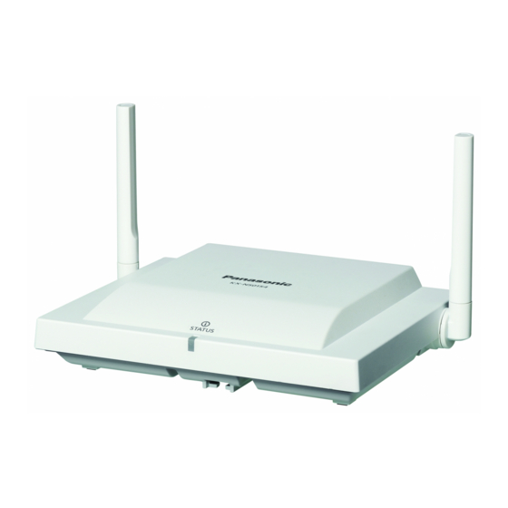
- Page 1 ORDER NO. KMS1411116CE DECT 4-Channel IP Cell Station Unit KX-NS0154 Model No. (for , U.S.A., Canada, Mexico) © Panasonic System Networks Co., Ltd. 2014 Unauthorized copying and distribution is a violation of law.
-
Page 2: Table Of Contents
KX-NS0154 TABLE OF CONTENTS PAGE PAGE 13.1. Main Board ------------------------------------------------ 27 1 Safety Precautions -----------------------------------------------3 1.1. For Service Technicians ----------------------------------3 13.1.1. No.1 ---------------------------------------------------- 27 1.2. Caution--------------------------------------------------------3 13.1.2. No.2 ---------------------------------------------------- 28 2 Warning --------------------------------------------------------------3 13.1.3. No.3 ---------------------------------------------------- 29 2.1. About Lead Free Solder (PbF: Pb free) --------------3 13.1.4. -
Page 3: Safety Precautions
KX-NS0154 1 Safety Precautions 1. Before servicing, unplug the AC power cord to prevent an electric shock. 2. When replacing parts, use only the manufacturer's recommended components. 3. Check the condition of the power cord. Replace if wear or damage is evident. -
Page 4: Suggested Pbf Solder
KX-NS0154 2.1.1. Suggested PbF Solder There are several types of PbF solder available commercially. While this product is manufactured using Tin, Silver, and Copper, (Sn+Ag+Cu), you can also use Tin and Copper, (Sn+Cu), or Tin, Zinc, and Bismuth, (Sn+Zn+Bi). Please check the manufac turer's specific instructions for the melting points of their products and any precautions for using their product with other materials. -
Page 5: Specifications
KX-NS0154 3 Specifications IP-CS Specification Items Description 4 channel CS Type Narrowband Supported Audio DECT Radio Method MGCP VoIP Signalling Protocol IP Port Number Flexible Setting Yes (through Web application) Local Setting Yes (through Web application) Site Survey Mode Yes (through Web application) -
Page 6: Technical Descriptions
KX-NS0154 4 Technical Descriptions 4.1. Block Diagram... -
Page 7: Main Processer
4.3. Power Supply Circuit KX-NS0154 support 2 way power supply; AC adaptor and PoE (Power over Ethernet). 9V is supplied from AC adaptor through JK701. 48V is supplied from ethernet through JK302, and it is converted to 12V by IC303. -
Page 8: Clock Circuit
KX-NS0154 4.5. Clock Circuit 4.5.1. System Clock Main system clock (13.824MHz) is generated from X501, and Oscillation circuit consists of X501 and IC501. This clock is used for basic clock of IC501's all internal clock and RF. This clock is supplied to IC100 and IC503 via buffer IC (IC704). -
Page 9: Rf Circuit
KX-NS0154 4.8. RF Circuit RF Transmission A digital audio signal and control signal from LAN is received by DVF99 (IC100) in a cell station. Then data goes to RFIC (IC501) through SPI and TDM signal, and it's modulated to 1.9 GHz RF signal. The RF signal is ampli- fied and fed to a selected antenna by antenna diversity. -
Page 10: Location Of Controls And Components
KX-NS0154 5 Location of Controls and Components 5.1. Names and Locations 6 Installation Instructions Refer to 16. Appendix (P.61). -
Page 11: Firmware Update
KX-NS0154 7 Firmware update 7.1. Firmware update The firmware of NS0154 is stored in NS1000 1. Log in to WEB MC of NS1000. 2. Select “Maintenance” “System Control” “1.Program Update” “1.Download Program File” “1.Manual” 3. The item of “Look in” is set as “Local PC”, and a firmware file name is specified. -
Page 12: Service Mode
KX-NS0154 8 Service Mode 8.1. How to Change MAC Address Label (Procedure after Replacing the Main P.C.B.) When replacing the Main P.C.B., customer data shall be renewed before sticking the included MAC/Address. 8.1.1. Replacing Main P.C.B. Note: (*1) : If you reuse defective P.C.B. for another repairing unit by repairing. Peel off the CS-ID and MAC address label on original bottom cabinet and keep them with defective P.C.B.. -
Page 13: Troubleshooting Guide
KX-NS0154 9 Troubleshooting Guide 9.1. No Power... -
Page 14: No Operation
KX-NS0154 9.2. No Operation Note: Refer to waveform (1) - (7) in Waveform (P.32) . (*1) Adjust clock after changing X201, X501, C237, C238, C556, C557. Refer to 11. Measurements and Adjustments (P.19) - Page 15 KX-NS0154 Note: Refer to waveform (8) - (11) in Waveform (P.33) .
- Page 16 KX-NS0154 Note: Refer to waveform (12) - (14) in Waveform (P.33) .
-
Page 17: System Check
KX-NS0154 9.3. System Check Note: Refer to waveform (15) - (18) in Waveform (P.33 and P.34) . -
Page 18: Disassembly And Assembly Instructions
KX-NS0154 10 Disassembly and Assembly Instructions 10.1. Disassembly Instructions 1. Remove the 4 screws (A), and remove the Bottom Cabinet. 2. Remove the Solder on Cable of the Main Board by the Soldering iron. 3. Remove the Main Board from the Top Cabinet. -
Page 19: Measurements And Adjustments
KX-NS0154 11 Measurements and Adjustments 11.1. USB Test Mode The various tests are avialbale by using USB communication with your PC. Following tests are described in this service manual. • Clock Adjustment (P.22) Note: Make sure that you have installed USB driver on your Windows PC before starting test mode. - Page 20 KX-NS0154 11.1.1.3. PC Setting Preparation: • PC • Base Unit / Handset 1. Install the TeraTerm Install the "teraterm-x.xx.exe" (x.xx = version) to your PC from internet site. Refer to the "readme" of the TeraTerm for installation process etc. 2. Setting the TeraTerm Before setting the TeraTarm: USB ports 3 to 16 are available but Teraterm (version 2.3) sets to use only the USB ports 3 and 4 by default.
- Page 21 KX-NS0154 2-3. Select "Save setup" from "Setup" menu and overwrite TERATERM.INI. Note: • Once you install USB driver and test mode application, it is unnecessary to do it again.
-
Page 22: Clock Adjustment
11.2. Clock Adjustment 1. Supply power fom AC adaptor. *Fig.1 2. Connect a USB cable to PC and KX-NS0154** after 10 seconds from Power on ... from Power on, then execute Teraterm on 3. Input User ID and Password. User ID : root Password : P!1230!N 4. -
Page 23: Miscellaneous
KX-NS0154 12 Miscellaneous 12.1. Terminal guide of ICs, Transistors and Diodes C0EBE0000444, C0DBGYY00905 C1ZBZ0003969 C1CB00004203 PNWIAS0154CE,PNWIBS0154CE, C1CB00003680 C2HBCY000134 B1CFNN000001 C0DBAYY00932, B1HBCFA00028 C0ABAA000068 PQVTDTC123E Anode Cathode Cathode Anode B3ABB0000296 B3AAB0000347 B3AEB0000153 Cathode Cathode Anode Anode B0JCML000007, B0BC06800004, DB2X41400L B0JCPL000004, B0JCNE000008 B0EDER000009... -
Page 24: How To Replace A Flat Package Ic
KX-NS0154 12.2. How To Replace a Flat Package IC Even if you do not have the special tools (for example, a spot heater) to remove the Flat IC, with some solder (large amount), a sol- dering iron and a cutter knife, you can easily remove the ICs that have more than 100 pins. -
Page 25: How To Replace The Llp (Leadless Leadframe Package) Ic And Ic Ground Plate
KX-NS0154 12.3. How to Replace the LLP (Leadless Leadframe Package) IC and IC ground plate 12.3.1. Preparation • PbF (: Pb free) Solder • Soldering Iron Tip Temperature of 700 F ± 20 F (370 C ± 10 C) Note: We recommend a 30 to 40 Watt soldering iron. -
Page 26: How To Remove A Solder Bridge (Doesn't Apply To Ic Ground Plate.)
KX-NS0154 12.3.5. How to Remove a Solder Bridge (Doesn't apply to IC ground plate.) When a Solder Bridge is found after soldering the bottom of the IC, remove it with a soldering iron. -
Page 27: Schematic Diagram
KX-NS0154 13 Schematic Diagram 13.1. Main Board 13.1.1. No.1... - Page 28 KX-NS0154 13.1.2. No.2...
- Page 29 KX-NS0154 13.1.3. No.3...
- Page 30 KX-NS0154 13.1.4. No.4...
- Page 31 KX-NS0154 13.1.5. No.5...
-
Page 32: Waveform
KX-NS0154 13.2. Waveform 13.2.1. No.(1)-(7) (1) RESET(IC201) (2) PCLK−DVF OSC=13.824MHz (IC100) Power on At the time of power supply ON RESET(Pin4) R211 13.824MHz (3) PLL CLK =13.824MHz (IC301) (4) RF IC CLK = 13.824MHz(IC501) R559(IC501 side) TP(PCLK) 13.824MHz 13.824MHz (5) RF OPAMP CLK =13.824MHz(IC704) -
Page 33: (8)-(15)
KX-NS0154 13.2.2. No.(8)-(15) (8)RF(IC501) RESET at Power ON (9)RF ROM IF(IC502) At the time of power supply ON At the time of power supply ON /CS(Pin1) R505 DO(Pin2) CLK(Pin6) (10)EC(IC503) RESET (11)EC ROM IF(IC504) At the time of power supply ON... -
Page 34: (16)-(18)
KX-NS0154 13.2.3. No. (16)-(18) (16)SPI EC(IC503)-DVF(IC100) (17)TDM RF(IC501)-DVF(IC100) At the time of power supply ON At the time of power supply ON DI(R549) CLK(R728) CLK(R727) FSYNC(R729) DO(R316) DTX(R317) DRX(R508) CS(R318) (18)TDM EC(IC503)-DVF(IC100) CLK(R732) FSYNC(R730) DTX(R731) DRX(R541) -
Page 35: Printed Circuit Board
C219 C218 C127 C210 R542 C229 L207 C230 L208 C225 L203 L101 C205 C106 C226 L204 R103 C228 L206 C113 C227 L205 C114 C110 C109 C115 C105 3.2V 1.85V C104 C107 C111 C112 C116 D101 KX-NS0154 MAIN BOARD Bottom View... -
Page 36: Bottom View
C357 L202 C310 USBP1 R729 USBN1 R106 USB_DG1 R110 R316 C118 KX-NS0154 C702 C103 C117 L701 R733 L702 R102 C716 C715 IC101 C714 C304 C713 C726 C727 JK301 C303 PNLB2296Z IC703 IC702 C728 C729 Q104 KX-NS0154 MAIN BOARD Component View... -
Page 37: Appendix Information Of Schematic Diagram
KX-NS0154 15 Appendix Information of Schematic Diagram Note: 1. DC voltage measurements are taken with an oscilloscope or a tester with a ground. 2. The schematic diagrams and circuit board may be modified at any time with the development of new technology. -
Page 38: Exploded View And Replacement Parts List
KX-NS0154 16 Exploded View and Replacement Parts List 16.1. IC Data 16.1.1. IC100 (DVF99) Pin No. Terminal Name Contents of Control I/O setting Remark MEMXA2_EXTINT4 not used MEMXA3_LCDGP0 not used DDR_REF2 DDR Reference Voltage Input DDRDQS1_N DDR Data Strobe 1 Negative... - Page 39 KX-NS0154 Pin No. Terminal Name Contents of Control I/O setting Remark MEMXA14_BA1_LCDD8 not used MEMXA16 not used DDRDQ9 DDR Data DDRDQ13 DDR Data DDRDQ15 DDR Data DDRDM0 DDR Data Mask DDRRST_N DDR Reset Active Low (Not used) DDRCKE DDR Clock Enable...
- Page 40 KX-NS0154 Pin No. Terminal Name Contents of Control I/O setting Remark PLL3_DVDD PLL3 Digital SPI1DI SPI2 Serial Data In JTAG Clock JTAG Data In EXTINT15_SYNCPORT IC501 SPI handshake RF_RADIO_EN_EXTINT9 IC503 SPI handshake MAIN_CLK_OUT DVF-DCX(IC503) handshake for SPI MEMXD8_LCDD12 PHY RESET...
- Page 41 KX-NS0154 Pin No. Terminal Name Contents of Control I/O setting Remark MEMXD2_LCDD4 Not used VDDIO_RGMII RGMII I/O VDDIO General I/O GND Connection GND Connection GND Connection GND Connection GND Connection GND Connection PLL3_AVDD PLL3 Analog IF_EN_AD TDM-DTX for IC503 IF_DATA_AD...
- Page 42 KX-NS0154 Pin No. Terminal Name Contents of Control I/O setting Remark VREF Reference Voltage Powered by VCCA for Filtering MICPWR0 Microphone Power 0 Output SINGIN1 Input of Single-ended In Amplifier 1 (Not used) DCIN2 DC A/D Input 2 (Not used)
- Page 43 KX-NS0154 Pin No. Terminal Name Contents of Control I/O setting Remark NFLCLE_MEMXA25 NFL Command Latch NFLD2_QDQ1 NFL Data EXTINT2_CLK_OUT GPIO (Not used) KEY_ROW4 Trace (Not used) KEY_COL3 DIP SW detect KEY_ROW5 Trace (Not used) SD_D0 SDMMC Data (Not used) RSTN...
-
Page 44: Ic101 (Ddr2)
KX-NS0154 16.1.2. IC101 (DDR2) Pin No. Terminal Name Contents of Control I/O setting Remark Power Supply No connect Ground VSSQ DQ Ground #UDQS Data Store VDDQ DQ Power Supply DQ14 Data Inputs/Outputs VSSQ DQ Ground Input Data Mask UDQS Data Store... - Page 45 KX-NS0154 VSSQ DQ Ground Data Inputs/Outputs Data Inputs/Outputs VSSQ DQ Ground Data Inputs/Outputs VDDL DLL Power Supply VREF Rference Voltage Ground VSSDL DLL Ground Clock Power Supply Clock Enable Command Inputs #RAS Command Inputs Clock On Die Termination No connect...
-
Page 46: Ic102 (Nand Flash Memory)
KX-NS0154 16.1.3. IC102 (NAND Flash Memory) Pin No. Terminal Name Contents of Control I/O setting Remark No connect No connect No connect No connect No connect No connect R/B# Ready/Busy Open-Drain Read Enable Chip Enable No connect No connect Core power supply... -
Page 47: Ic302 (Phy)
KX-NS0154 16.1.4. IC302 (PHY) Pin No. Terminal Name Contents of Control I/O setting Remark EXTRES Connect to GND via 12.4kɹ resistor TEST (Not used) P0TXP LAN Interface Positive Output P0TXN LAN Interface Negative Output P0AGND1 Analog GND P0RXP LAN Interface Positive Intput... -
Page 48: Ic501 (Dcx81 (Rf & Dsp))
KX-NS0154 16.1.5. IC501 (DCX81 (RF & DSP)) Pin No. Terminal Name Contents of Control I/O setting Remark QSPI data pin 2 QSPI data pin 0 GPIO26 / XD3 GPIO Output (Not used) GPIO27 / XD2 GPIO Output (Not used) I/O supply voltage... - Page 49 KX-NS0154 VCC_FE_IF FE & IF supply VCC_PA PA supply BAL_OUT2 Balun output P BAL_OUT1 Balun output N TX_SW DPDT switch Tx input ANT1 Antenna 1 port GND_RF RF ground ANT2 Antenna 2 port TEST Test mode control RX_SW DPDT switch Rx output...
-
Page 50: Ic502 (Serial Flash Memory)
KX-NS0154 16.1.6. IC502 (Serial Flash Memory) Pin No. Terminal Name Contents of Control I/O setting Remark Chip select Serial data W# / Vpp / DQ2 Serial data Ground Serial data Clock HOLD#/DQ3 Serial data Device core power supply... -
Page 51: Ic503 (Dcx81 (Dsp))
KX-NS0154 16.1.7. IC503 (DCX81 (DSP)) Pin No. Terminal Name Contents of Control I/O setting Remark QSPI data pin 2 QSPI data pin 0 GPIO26 / XD3 GPIO Output (Not used) GPIO27 / XD2 GPIO Output (Not used) I/O supply voltage... - Page 52 KX-NS0154 VCC_PA PA Supply BAL_OUT2 Not used BAL_OUT1 Not used TX_SW Not used ANT1 Not used GND_RF RF ground ANT2 Not used TEST Not used RX_SW Not used LNA_INN Not used LNA_INP Not used ATST_N Analog test N (Not used)
-
Page 53: Ic504 (Serial Flas Memory)
KX-NS0154 16.1.8. IC504 (Serial Flas Memory) Pin No. Terminal Name Contents of Control I/O setting Chip select Serial data W# / Vpp / DQ2 Serial data Ground Serial data Clock HOLD#/DQ3 Serial data Device core power supply... -
Page 54: Cabinet And Electrical Parts Location
KX-NS0154 16.2. Cabinet and Electrical Parts Location PCB1 SCREW Ref. No. Figure (Φ 26x14mm) -
Page 55: Accessories And Packing Material
KX-NS0154 16.3. Accessories and Packing Material... -
Page 56: Replacement Parts List
KX-NS0154 16.4. Replacement Parts List 16.4.2. Accessory and Packing Materials Note: Safety Ref. Part No. Part Name & Description Remarks 1. RTL (Retention Time Limited) The marking (RTL) indicates that the Retention Time is PQHE5004Y SCREW XWG35FJ WASHER limited for this item. - Page 57 KX-NS0154 Safety Ref. Part No. Part Name & Description Remarks Safety Ref. Part No. Part Name & Description Remarks L211 J0JBC0000107 IC FILTER L301 J0JBC0000107 IC FILTER (RESISTORS) L302 J0JBC0000107 IC FILTER L201 ERJ2GE0R00 L303 J0JBC0000107 IC FILTER L508 ERJ2GE0R00...
- Page 58 KX-NS0154 Safety Ref. Part No. Part Name & Description Remarks Safety Ref. Part No. Part Name & Description Remarks R341 ERJ2GEJ511 R710 ERJ2GEJ104 100k R342 ERJ2GEJ103 R711 ERJ2GEJ104 100k R343 ERJ2RKF1242 12.4k R712 ERJ2RKF4701 4.7k R344 ERJ12YJ390H R713 ERJ2RKF3901X 3.9k...
- Page 59 KX-NS0154 Safety Ref. Part No. Part Name & Description Remarks Safety Ref. Part No. Part Name & Description Remarks C223 ECUE1C104KBQ C508 ECUV1A225KBV C224 ECUE1C104KBQ C509 ECUE1H100DCQ C225 ECUE1C104KBQ C510 ECUE1H100DCQ C226 ECUE1C104KBQ C511 ECUE1H1R5CCQ C227 ECUE1C104KBQ C512 ECUE1H1R5CCQ C228...
- Page 60 KX-NS0154 Safety Ref. Part No. Part Name & Description Remarks (FUSES) F301 K5H302Y00003 FUSE F302 K5H302Y00003 FUSE F701 K5H312200002 FUSE (OTHER) PNMC1106Z MAGNETIC SHIELD...
-
Page 61: Appendix
KX-NS0154 17 Appendix The extract from an Operating Instructions. KXNS0154... - Page 62 2 Overview LED Indications Color Status Green (4 channels — Stand-by (no active calls) without activation Slow Flashing Talking (active calls, channels available) Moderate Flashing All channels busy Blue (8 channels — Stand-by (no active calls) with activation key Slow Flashing Talking (active calls, channels available) Moderate Flashing All channels busy...
- Page 63 You can download the Site Planning Tool from the following Web site to estimate the number of CSs required for your installation area and their approximate installation locations. http://panasonic.net/pcc/support/pbx/ The Site Planning Tool for LAN synchronization is different from the Site Planning Tool for Air synchronization.
- Page 64 3 Deployment Procedure Pass the cable through the groove of the unit in one of the following three ways. To a Switching Hub/PoE To a Switching Hub/PoE To a Switching Hub/PoE Connecting the AC adaptor cord to the unit Installation Guide...
- Page 65 3 Deployment Procedure Pass the cord through the groove of the unit in one of the following three ways. To AC Adaptor To AC Adaptor To AC Adaptor Connecting the Unit to the Network Temporarily install the unit in the best site as defined in Site Planning, connect the unit to a nearby hub. [LAN Synchronization only] LAN synchronization should be diagnosed in advance when connecting to a network that does not comply with recommendations 1 and 2 in "5.3 Recommended Network Configuration".