Advertisement
CONTENTS(目次)
SPECIFICATIONS (総合仕様) ....................................3
PANEL LAYOUT ( パネルレイアウ ト) ..............................6
DIMENSIONS (寸法図) ...............................................7
JACK AND PLUG LIST ( 端子と プラ グ一覧) ..................8
CIRCUIT BOARD LAYOUT ( ユニ ッ ト レ イ アウ ト) ..............9
DISASSEMBLY PROCEDURE (分解手順) ............... 10
LSI PIN DESCRIPTION (LSI端子機能表) ................. 18
CIRCUIT BOARDS (シー ト基板図) .............................21
INSPECTION (検査) ............................................32/61
MEASUREMENT ( 測定) ......................................53/82
UPDATING FIRMWARE (ファームウ ェアのアッ プデー ト) ...60/89
DEVICE BACKUP (デバイ ス バッ クアッ プ) ..................90
PA
012180
POWER AMPLIFIER
SERVICE MANUAL
SERVICE MANUAL
(PXアンプの初期化) ..................................................92
FUNCTION LIST ( 機能一覧) .......................................94
MESSAGE LIST ( メ ッ セー ジ リ ス ト) . ...........................96/97
START-UP SEQUENCE (起動シーケンス) ........... 99/100
ENDING SEQUENCE (終了シーケンス) .............101/102
PARTS LIST
BLOCK DIAGRAM (ブロ ッ クダイアグラム)
LEVEL DIAGRAM (レベルダイアグラム)
WIRING (結線図)
CIRCUIT DIAGRAM (回路図)
Copyright (c) Yamaha Corporation. All rights reserved. PDF
PX10
PX8
PX5
PX3
HAMAMATSU, JAPAN
'16.10
Advertisement
Chapters

Related Manuals for Yamaha PX10


Summary of Contents for Yamaha PX10
-
Page 1: Table Of Contents
INSPECTION (検査) ..........32/61 LEVEL DIAGRAM (レベルダイアグラム) MEASUREMENT ( 測定) ........53/82 WIRING (結線図) UPDATING FIRMWARE (ファームウ ェアのアッ プデー ト) ...60/89 CIRCUIT DIAGRAM (回路図) DEVICE BACKUP (デバイ ス バッ クアッ プ) ....90 012180 HAMAMATSU, JAPAN Copyright (c) Yamaha Corporation. All rights reserved. PDF ’16.10... - Page 2 IMPORTANT NOTICE This manual has been provided for the use of authorized Yamaha Retailers and their service personnel. It has been assumed that basic ser- vice procedures inherent to the industry, and more specifically Yamaha Products, are already known and understood by the users, and have therefore not been restated.
-
Page 3: Specifications(総合仕様
1.5 msec User Amplifier Preset(ユーザーアンププリセット) 8 user amplifier presets Factory Speaker Preset (出荷時スピーカープリセット) Speaker presets for Yamaha passive speakers Analog input XLR-3-31 × 2, 1/4" PHONE(TRS) × 2 Speakers Neutrik speakON NL4 × 2, binding post × 2 pairs, 1/4" PHONE(TS) × 2 Connectors (端子)... - Page 4 PX10/PX8/PX5/PX3 • Current draw and thermal dissipation (消費電流と熱放散) Test signal: Pink noise (bandwidth limited from 22 Hz to 22 kHz), 1 Btu = 1,055.06 J = 0.252 kcal, (W) × 0.86 = kcal (テスト信号:ピンクノイズ (22 Hz から 22 kHz に帯域制限 )、1 BTU = 1,055.06 J = 0.252 kcal、1 W = 0.86 kcal) PX10 ● Line current (A) Watt (W) Thermal dissipation (線電流) (電力) (熱放散) 100 V/50 Hz Power consumption (In) Power consumption (Out) Watts dissipated 100 V Btu/h kcal/h (消費電力)...
- Page 5 PX10/PX8/PX5/PX3 ● Line current (A) Watt (W) Thermal dissipation (線電流) (電力) (熱放散) 100 V/50 Hz Power consumption (In) Power consumption (Out) Watts dissipated 100 V Btu/h kcal/h (消費電力) (消費電力) (放散電力) Idle (アイ ドル) 8Ω/ch 1/8 out 4Ω/ch 8Ω/ch 1/3 out 4Ω/ch...
-
Page 6: Panel Layout(パネルレイアウト
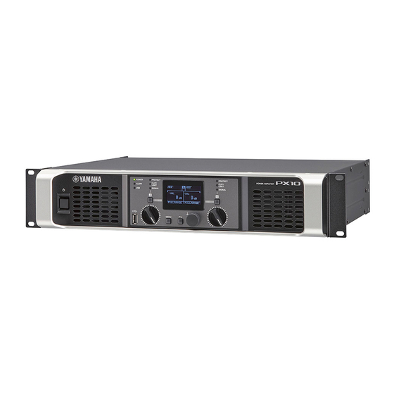
PX10/PX8/PX5/PX3 PANEL LAYOUT(パネルレイアウト) • Front Panel (フロントパネル) q Power button q 電源ボタン w [POWER] indicator w [POWER]インジケーター e [ALERT] indicator e [ALERT]インジケーター r [USB] indicator r [USB]インジケーター t [CLIP/LIMIT] indicators t [CLIP/LIMIT]インジケーター y [SIGNAL] indicators y [SIGNAL]インジケーター u [PROTECT] indicators u [PROTECT]インジケーター... -
Page 7: Dimensions(寸法図
PX10/PX8/PX5/PX3 • Rear Panel (リアパネル) !6 [INPUT] A/B connectors !6 [INPUT] A/B端子 !7 [SPEAKERS] A/B terminals !7 [SPEAKERS] A/B端子 !8 AC IN connector !8 AC IN端子 !9 Exhaust ports !9 排気口 DIMENSIONS(寸法図) unit : mm (単位)... -
Page 8: Jack And Plug List(端子とプラグ一覧
PX10/PX8/PX5/PX3 JACK AND PLUG LIST(端子とプラグ一覧) • XLR jack ( XLR端子) • Binding post connector (バインディングポスト端子) XLR type 3-31 jack. (XLR型3-31タイプの端子です。 ) • Without plugs ( プラグなしの場合) Remove about 15 mm of insulation from the end of each The polarity is shown below (IEC60268). -
Page 9: Circuit Board Layout(ユニットレイアウト
PX10/PX8/PX5/PX3 CIRCUIT BOARD LAYOUT(ユニットレイアウト) • Top view (上から見た図) AC INLET (ACインレッ ト) AUDIO ACIN DC FAN DC FAN (DCファ ン) (DCファ ン) • Front view (前面から見た図)... -
Page 10: Disassembly Procedure(分解手順
PX10/PX8/PX5/PX3 DISASSEMBLY PROCEDURE(分解手順) Caution: 注意事項 • Install the binding tie and the cord clamp in the same way • インシュロックタイ、 束線止めは、 取り外す前と同じように取り as they were before removal. 付けてください。 • Pay attention not to insert and install the FFC cable to the • FFCケーブルの表... - Page 11 PX10/PX8/PX5/PX3 <Top view (上面) > AC INLET Priority screw (2nd) (ACインレット) (優先ネ ジ 2) [350] [860] [440] [520] [440] Priority screw (1st) (優先ネ ジ 1) AUDIO CB902 CB901 [340] ACIN [630] Priority screw (2nd) Priority screw (1st) (優先ネ ジ 2) [470A] [520] (優先ネ ジ 1)...
- Page 12 OUT circuit board. (Fig. 2) 5-4 PSシートを外します。 ( 3 項参照) Remove the PS circuit board. (See procedure 3.) 5-5 PX10/PX8 のみ PX10/PX8 only [850]のプラスチックリベット 2 個を外して、 ダクト Remove the two (2) plastic rivets marked [850]. The duct AMPを外します。 ( 図4)...
- Page 13 PX10/PX8/PX5/PX3 Set AUDIO circuit board with bending FFC guard. (FFCガー ド を曲げながらAUDIOシー ト を取り付けて く だ さ い。 ) [850] DUCT AMP (ダク トAMP) FFC GUARD (FFCガー ド) Fit the tabs of duct amp into the slots of sub chassis.
- Page 14 PX10/PX8/PX5/PX3 Priority screw (1st) (優先ネ ジ 1) Priority screw (3rd) [100] (優先ネ ジ 3) Priority screw (1st) Priority screw (4th) (優先ネ ジ 1) (優先ネ ジ 4) [960] POWER SWITCH KNOB (PSWノ ブ) Priority screw (2nd) (優先ネ ジ 2) FRONT PANEL [940] ASSEMBLY (FパネルAss y) KNOB ENCDR (ノ...
- Page 15 PX10/PX8/PX5/PX3 <Rear view (背面) > Priority screw (1st) [720] (優先ネ ジ 1) Priority screw (3rd) (優先ネ ジ 3) SHIELD ACIN (シール ドACIN) [720] Priority screw (2nd) (優先ネ ジ 2) RACK ANGLE (ラ ッ ク金具) [1020] [750] Priority screw (2nd) Priority screw (3rd) (優先ネ ジ 2)...
- Page 16 PX10/PX8/PX5/PX3 FFC GUARD : PX5/PX3 onry (FFCガー ド : PX5/PX3のみ) [40] DC FAN (DCファ ン) DC FAN (DCファ ン) [40] HOLDER FFC (ホルダーFFC) FPN CS (with ENC circuit board) [880] Priority screw (2nd) (優先ネ ジ 2) [80] [90] [140] HEXAGONAL NUT Attach the holder FFC so as to match (六角ナッ...
- Page 17 PX10/PX8/PX5/PX3 DC FAN 12. DCファン (所要時間 : 約9 分) (Time required: About 9 minutes) 12-1 Remove the eight (8) screws marked [40]. The DC fans 12-1 [40]のネジ 8 本を外して、 左右のDCファンを外しま can then be removed. (Fig. 8) す。 ( 図8) Remove the along with the FFC guard is the PX5 / PX3.
-
Page 18: Lsi Pin Description (Lsi端子機能表
PX10/PX8/PX5/PX3 LSI PIN DESCRIPTION(LSI 端子機能表) AK4382AVT (X0661A00) DAC (Digital to Analog Converter) ............... 18 LPC1820FBD144,551 (YF570B00) MCU (Microcontroller Unit) ............19 NJW1194V(TE1) (X8355A00) 2-CHANNEL ELECTRONIC VOLUME ..........18 PCM1804DBR (X6872A01) ADC (Analog to Digital Converter) ............18 YDA177-VZ (YF978A00) DIGITAL POWER AMPLIFIER ..............20 YSS952-QZE2A (YE441A00) DSP(SPR-2) (Digital Signal Processor) ..........20... - Page 19 PX10/PX8/PX5/PX3 LPC1820FBD144, 551 (YF570B00) MCU (Microcontroller Unit) FPN (PN) : IC103 NAME FUNCTION NAME FUNCTION General purpose digital input/output pin I2S0_RX_MCLK S receive master clock GPIO2 ADC input channel 1 I2S0_RX_WS Receive Word Select ADC0_1 General purpose digital input/output pin...
- Page 20 PX10/PX8/PX5/PX3 YSS952-QZE2A (YE441A00) DSP (SPR-2) (Digital Signal Processor) AUDIO: IC410 NAME FUNCTION NAME FUNCTION GPIO5 OPEN Leave this pin open GPIO4 General-purpose I/O pins DVSS GPIO3 IRQ_N Interrupt request output pin to the host controller DVDD18 Core power supply DVSS...
-
Page 21: Circuit Boards (シー ト基板図
PX10/PX8/PX5/PX3 CIRCUIT BOARDS(シート基板図) ACIN Circuit Board (YG871D0) ........22/23 AUDIO Circuit Board (YG852E0) ........24/25 ENC (PN) Circuit Board (YH533B0) ........21 FPN (PN) Circuit Board (YH533B0)........26 OUT Circuit Board (YG853E0) ..........27 PF (PN) Circuit Board (YH533B0) ......... 30 PS Circuit Board (YG872D0) .......... -
Page 22: Acin Circuit Board (Yg871D0)
PX10/PX8/PX5/PX3 ACIN Circuit Board to PS-CB209 to PSW-W302A/B/C to PS-CB208 A’ AC-INLET A’ Component side (部品側) 2NA-ZT09720... - Page 23 PX10/PX8/PX5/PX3 ACIN Circuit Board B’ B’ Pattern side (パターン側) 2NA-ZT09720...
-
Page 24: Audio Circuit Board (Yg852E0)
PX10/PX8/PX5/PX3 Scale: 80/100 AUDIO Circuit Board INPUT A INPUT B to PF-CB405 Component side (部品側) 2NA-ZT09660... - Page 25 PX10/PX8/PX5/PX3 Scale: 80/100 AUDIO Circuit Board Pattern side (パターン側) 2NA-ZT09660...
-
Page 26: Fpn (Pn) Circuit Board (Yh533B0)
PX10/PX8/PX5/PX3 FPN (PN) Circuit Board to USB-CB306 to ENC-CB302 Component side (部品側) to AUDIO-CB402 N.C. N.C. not installed to VOL-W301 to PF-W401 to DISPLAY Pattern side (パターン側) 2NA-ZT09640... -
Page 27: Out Circuit Board (Yg853E0)
PX10/PX8/PX5/PX3 OUT Circuit Board SPEAKERS A SPEAKERS B to AUDIO-W801A/B/C/D to AUDIO-W802A/B/C/D Component side (部品側) Pattern side (パターン側) 2NA-ZT09710... -
Page 28: Ps Circuit Board (Yg872D0)
PX10/PX8/PX5/PX3 PS Circuit Board to AUDIO-CB802 to AUDIO-CB806 to PF-CB401 to AUDIO-CB801 to ACIN-CB102 to ACIN-CB101 Component side (部品側) 2NA-ZT09780... - Page 29 PX10/PX8/PX5/PX3 PS Circuit Board Pattern side (パターン側) 2NA-ZT09780...
-
Page 30: Pf (Pn) Circuit Board (Yh533B0)
PX10/PX8/PX5/PX3 PF (PN) Circuit Board to PS-W203 to AUDIO-W401 to DC FAN to DC FAN to FPN-CB304 Component side (部品側) Pattern side (パターン側) USB (PN) Circuit Board to FPN-CB106 Component side (部品側) Pattern side (パターン側) 2NA-ZT09640... -
Page 31: Vol (Sub) Circuit Board (Yg978E0)
PX10/PX8/PX5/PX3 VOL (SUB) Circuit Board VOLUME A VOLUME B to FPN-CB103 Component side (部品側) Pattern side (パターン側) 2NA-ZT09940... -
Page 32: Inspection (検査
PX10/PX8/PX5/PX3 INSPECTION Preparation Modes for Activation 1-1. Equipment 2-1. Service inspection mode • USB Memory This activation mode is to perform Service inspection. • Connect a FAT32 formatted USB2.0 memory Turn on while pushing the [MENU] key, the [A] key and the [B] key simultaneously. - Page 33 PX10/PX8/PX5/PX3 Service inspection 4-1. How to connect Refer to the “1-2. How to connect” (Page 32) of Inspection section. 4-2. How to activate Refer to the “2-1. Service inspection mode” (Page 32) of Inspection section. If powered on with service inspection mode successfully, during Power On sequence, all LEDs light up simultaneously for a few seconds.
- Page 34 PX10/PX8/PX5/PX3 Inspection item 5-1. USB 5-2. Information 5-1-1. USB Bus, USB0-ID 5-2-1. Firmware version Contents The state of FAT32 fi le system currently recorded on Contents A version number inspects visual agreement. the USB memory is inspected. Advance preparation None. Advance preparation Confi...
- Page 35 PX10/PX8/PX5/PX3 5-2-3. AUDIO-ID 5-2-6. PS-ID0 Variable (PCB PN Assembly only) Contents An AUDIO-ID inspects automatically that it is in This is not tested for service inspection of PX amplifi er. agreement with an expected value. Advance preparation None. 5-2-7. PS-ID1 Contents An PS-ID1(from PCB PS) inspects visually agreeing 〈...
- Page 36 PX10/PX8/PX5/PX3 5-3. Statistics (Service only) 5-3-1. Browsing 5-3-2. Clear Contents The operating condition statistic of amplifier is Contents After exchanging the following parts, a related inspected visually. statistic is cleared manually. Refer to Statistics list. Exchanged parts Item to clear...
- Page 37 PX10/PX8/PX5/PX3 5-4. DP200 (IC601) 5-4-1. I2C Bus 5-4-4. V-SENSE OUTVA,OUTVB Contents Via I2C Bus which is a communication path with a Contents When the output voltage of amplifier without load microcomputer, it inspects automatically using the is normal, it inspects automatically that the value register of DP200.
- Page 38 PX10/PX8/PX5/PX3 5-4-9. /CLIP-B OFF 5-4-5. I-SENSE OUTIA,OUTIB Contents When the output current of amplifier with rated This is not tested for service inspection of PX amplifi er. load is normal, it inspects automatically that the value of the OUTIA or OUTIB register of DP200 is 5-4-10.
- Page 39 PX10/PX8/PX5/PX3 5-5. Temperature 5-6. SPI Flash (IC104) 5-6-1. SPI Bus 5-5-1. AMP-A OTP_PS Flag PROT*_N Contents Read JEDEC ID (9Fh) command is written to the This is not tested for service inspection of PX amplifi er. SPI Flash device for data (IC104), and it inspects automatically that the following ID can be read.
- Page 40 PX10/PX8/PX5/PX3 5-7. DSP (IC104) 5-7-1. I2C Bus 5-7-2. /DSP-IRQ Contents Via I2C Bus which is a communication path with a Contents The function to assert a /DSP-IRQ signal is microcomputer, it inspects automatically using the automatically inspected via the register of DSP.
- Page 41 PX10/PX8/PX5/PX3 5-8. Analog 5-7-3. DSP-STATUS 5-8-1. /CFG1 (+14dBu) Contents The function to monitor a DSP-STATUS signal is Contents Measure the output characteristic of ChA/ChB on automatically inspected via the register of DSP. condition of the following. PX10 Advance preparation None. Input Sensitivity...
- Page 42 PX10/PX8/PX5/PX3 5-8-2. CFG2 (+4dBu) 5-8-3. CFG3 (Minimum volume) Contents Measure the output characteristic of ChA/ChB on Contents Measure the output characteristic of ChA/ChB on condition of the following. condition of the following. PX10 PX10 Input Sensitivity +4dBu Input Sensitivity +14dBu...
- Page 43 PX10/PX8/PX5/PX3 5-8-4. CFG4 (Boost mode) 5-8-5. /DSP-MUTE ON Contents Measure the output characteristic of ChA/ChB on Contents Measure the output level in the state where the condition of the following. /DSP-MUTE signal was asserted. PX10 Regarding criteria for measurement, refer to “2-2. inspection”...
- Page 44 PX10/PX8/PX5/PX3 5-9. LCD 5-8-6. /DSP-MUTE OFF 5-9-1. Parallel Bus Contents Measure the output level in the state where the Contents A parallel bus is automatically inspected by writing, /DSP-MUTE signal was negated. reading, comparing with the LCDC display data RAM in the LCD module on the following two Regarding criteria for measurement, refer to “2-2.
- Page 45 PX10/PX8/PX5/PX3 5-9-2. Panel 5-9-3. LCD-CONT (Contrast, Service Only) Contents Inspect the LCD panel visually. Contents Inspect the LCD contrast visually. The following 16 patterns are displayed every 400 Confirm the change of the minimum → maximum msec. → center luminance visually.
- Page 46 PX10/PX8/PX5/PX3 5-10. FAN 5-9-4. LCD-BL (Backlight) 5-10-1. Turn (Final Assy only) Contents Inspect the LCD backlight visually. This is not tested for service inspection of PX amplifi er. Confirm the change of the minimum → maximum → center luminance visually.
- Page 47 PX10/PX8/PX5/PX3 5-11. LED 5-10-3. Minimum speed 5-11-1. In order Contents In service inspection mode : It inspects rotating Contents Inspect visually as follows. visually 1) In order of the following, observe the LED lights up every 400msec. Advance preparation None. 〈 Service inspection screen 〉...
- Page 48 PX10/PX8/PX5/PX3 5-12. Tact switch 5-12-1. In order Contents According to directions of a screen, a semiautomatic inspection is conducted by pushing fi ve switches in following order. It is failure, when the switch which should be pushed on the next is not displayed after pushing a switch, or...
- Page 49 PX10/PX8/PX5/PX3 5-13. Rotary encoder 5-13-1. Rotate Left 5-13-2. Rotate Left Contents A semiautomatic inspection is conducted by turning Contents A semiautomatic inspection is conducted by turning a rotary encoder to the three lefts (counterclockwise a rotary encoder to the three rights (clockwise rotation).
- Page 50 PX10/PX8/PX5/PX3 5-14. Rotary potentiometer 3) If SIGNAL LED of both A/B lights up, it means that voltage 5-14-1. VOL-ALT positive acquisition of this position was completed. This is not tested for service inspection of PX amplifi er. 5-14-2.VOL-ALT negative This is not tested for service inspection of PX amplifi er.
- Page 51 PX10/PX8/PX5/PX3 When a [BACK] switch is pushed: When it returns to a maximum position: The fault location at the time of FAIL VR301, VR302 5-14-4.Confirm & Save 2 Contents In “5-14-3. Calibration 2”, it is inspected semi- automatically whether the voltage value read for every click is right.
- Page 52 PX10/PX8/PX5/PX3 2) The index of the rotary potentiometer of both A/B is aligned 5-15 Power off with the minimum position as follows. Contents Inspect the shutdown of the power supply when It will end, if the both SIGNAL LED lights up.
-
Page 53: Measurement ( 測定
PX10/PX8/PX5/PX3 MEASUREMENT Measurement condition 1-1. Environment 1-4. Caution for measurement environment Normal temperature: 5 to 40 degrees Connected chart when classD amplifi er (PX amplifi er) is Normal humidity: 30 to 90% measure Note) [the following measurement conditions are permitted if measurement result is in the inspection Insert AUX-0025 between classD amplifi... - Page 54 PX10/PX8/PX5/PX3 Therefore, the connection method with the interchangeability Flow of signal and output method of PX amplifi er that can correspond to any amplifier output method is preferable. The above-mentioned connection method can be compatible for the amplifier output with the single end output and the bridge output, and apply any audio analyzer.
- Page 55 ② THD=0.1% or less. When the sine wave of 1kHz is input to the input terminal, and the following table outputs are obtained, total harmonics distortion is measured. ① PX10 500W 38.3dBu ② PX10 10W 21.3dBu PX8 400W 37.3dBu PX8 10W 21.3dBu PX5 250W 35.3dBu...
- Page 56 PX10/PX8/PX5/PX3 2-2-5. DSP-MUTE noise level Measurement condition Criteria All channel Select “Analog > CFG1 ( +14dBu ) ” with Service inspection mode. PX10 -52dBu or less Measured mode / 8Ω MODE -53dBu or less -54dBu or less The signal of -10dBu is input to input terminal.
- Page 57 PX10/PX8/PX5/PX3 2-2-8. DP200 V-SENSE,I-SENSE Calibration Measurement condition Criteria Select “Analog > CFG1 ( +14dBu ) ” with Service inspection mode. The test program judge ‘PASS’ or ‘FAIL’ automatically. Measured mode / 8Ω MODE ※ When the calibration is completed successfully, it is outputted as PASS.
- Page 58 PX10/PX8/PX5/PX3 2-2-12. Maximum Output ( STEREO Mode ) ( 8Ω Mode/1 channel drive ) Measurement condition Criteria All channel Select “Analog > CFG1 ( +14dBu ) ” with Service inspection mode. PX10 More than 253Vp-p Measured mode / 8Ω MODE...
- Page 59 PX10/PX8/PX5/PX3 Setups at the time of maximum output measurement This item shall be tested with each measurement condition load resistances for each output terminals. The burst signal described in the following fi gure is applied to each input terminals.
-
Page 60: Updating Firmware (ファームウ ェアのアッ プデー ト
PX10/PX8/PX5/PX3 UPDATAING FIRMWARE Preparation 1-1. Equipment 1-4. Attention You must not turn off the power supply of PX amplifier • USB Memory (FAT32 or FAT16 format) until update is completed. When you turn on the power supply of PX amplifier on ※ Copy the fi rmware fi le ( PX̲PROG.BIN) to the ... - Page 61 PX10/PX8/PX5/PX3 検査 1. 準備 2. 起動モード 1-1. 機材 2-1. サービス検査モード • USBメモリー このモードは、 サービス検査用です。 • FAT32フォーマットされたUSB2.0メモリー [MENU]キー、 [A]キー、 [B]キーを同時に押した状態で 電源を入れます。 1-2. 接続方法 接続図 USBメモリーをパネル上のUSBポートに差します。 [A] キー [B] キー [MENU] キー [ ] (バッ ク) キー メ イ ンノ ブ 3. 検査項目一覧 ※ ○ : 検査する/× : 検査しない...
- Page 62 PX10/PX8/PX5/PX3 4. サービス検査 4-1. 接続方法 検査の 「1-2. 接続方法」 ( 61ページ) を参照してくださ い。 4-2. 起動方法 検査の 「2-1. サー ビス検査モー ド」 ( 61ページ) を参照して く だ さ い。 サー ビス検査モー ド に移行する と、 すべてのLEDが数秒間 同時に点灯し ます。 4-3. 検査画面 本体LCD。 カテゴ リ 選択画面。...
- Page 63 PX10/PX8/PX5/PX3 5. 検査項目 5-1. USB 5-2. Information 5-1-1. USB Bus, USB0-ID 5-2-1. Firmware version 内容 USBメモリーに記録されているFAT32ファイルシ 内容 ファームウェアバージョンの目視検査をします。 ステムの状態を検査します。 事前準備 なし。 事前準備 USBメモリーが装着されていることを確認しま す。 〈サービス検査画面〉 〈サービス検査画面〉 目視確認します。 FAIL時の故障個所 ファームウェアが正しくバージョンアップされていま せん。 5-2-2. SERIES-ID 内容 PCB PNからのSERIES-IDを目視検査します。 事前準備 なし。 〈サービス検査画面〉 FAIL時の故障個所 USB Bus(USB-DP, USB-DN, VBUS-EN, IC301, IC302), USB0-ID 5-1-2. VBUS (PCB PN Assy only)...
- Page 64 PX10/PX8/PX5/PX3 5-2-3. AUDIO-ID 5-2-6. PS-ID0 Variable ( PCB PN Assy only) 内容 PCB AUDIOからのAUDIO-IDと、 期待値との合致を サービス検査では実施しません。 自動検査します。 事前準備 なし。 5-2-7. PS-ID1 内容 PCB PSからのPS-ID1と、 PX本体の仕向けとの合致 〈サービス検査画面〉 を目視します。 事前準備 なし。 〈サービス検査画面〉 パネル印刷されたモデル名と合致するか、 目視確認します。 FAIL時の故障個所 接続されているPCB AUDIOの種別が違います。 以下の表を使用して、 PX本体の仕向けと合致するか目視確 または、 AUDIO-ID周辺回路の故障です。 認します。 PS-ID1 仕向け European model 5-2-4. AUDIO-ID Variable ( PCB PN Assy only) British model サービス検査では実施しません。 Korean model Chinese model U.S.A. model...
- Page 65 PX10/PX8/PX5/PX3 5-3. 統計 (サービス検査専用) 5-3-1. Browsing 5-3-2. Clear 内容 アンプの使用状況統計値を、 目視で確認します。 内容 以下の部品交換に伴い、 関連する統計値を手動でク 統計値一覧を参照します。 リアします。 交換部品 クリア対象 統計値一覧 パラメータ 意味 クリア対象 SW301 Rotary encoder 回転回数 Power ON 電源オン回数 VR301 Rotary potentiometer 回転回数 Encoder 回転回数 VR302 Rotary potentiometer 回転回数 Attenuator-A 回転回数 Attenuator-B 回転回数 PCB PS /PS-HI-TEMP 回数...
- Page 66 PX10/PX8/PX5/PX3 5-4. DP200 ( IC601) 5-4-1. I2C Bus 5-4-4. V-SENSE (OUTVA,OUTVB) 内容 マイコンとの通信経路であるI2Cバス経由で、 DP200 内容 無負荷アンプ出力が規定電圧を出力している状態に のレジスタを用い自動検査します。 おいて、 DP200のOUTVAレジスタ及びOUTVBレジ スタの値が判定範囲内であることを自動検査しま 事前準備 なし。 す。 〈サービス検査画面〉 事前準備 1. PXアンプの出力端子に8Ωのダミー抵抗を接 続します。 2. 正弦波 1kHzをPXアンプの入力端子に入力し ます。 3. アンプ出力を250W@8Ωに調整します。 〈サービス検査画面〉 左端の✽は、 選択カーソルです。 左端の✽は、 選択カーソルです。 FAIL時の故障個所...
- Page 67 PX10/PX8/PX5/PX3 5-4-5. I-SENSE (OUTIA,OUTIB) 5-4-10. V-SENSE,I-SENSE Calibration 内容 定格負荷アンプ出力が規定電流を出力している状態 内容 この検査は、 A、 Bごとに分けて、 実行します。 において、 DP200のOUTIAレジスタ及びOUTIBレ 無負荷アンプ出力が規定電圧を出力し、 定格負荷ア ジスタの値が判定範囲内であることを自動検査しま ンプ出力が規定電流を出力している状態において、 す。 DP200のOUTVxレジスタとOUTIxレジスタの値を 同時にキャリブレーションして、 それぞれの補正値を 事前準備 1. PXアンプの出力端子に8Ωのダミー抵抗を接 自動計算します。 補正値はFlashメモリに保存します。 続します。 (x=AまたはB) 2. 正弦波 1kHzをPXアンプの入力端子に入力し ます。 事前準備 1. PXアンプの出力端子に8Ωのダミー抵抗を接 ...
- Page 68 PX10/PX8/PX5/PX3 5-5. Temperature 5-6. SPI Flash ( IC104) 5-5-1. AMP-A (OTP̲PS Flag PROT*̲N) 5-6-1. SPI Bus サービス検査では実施しません。 内容 データ用SPI Flash(IC104)に、 Read JEDEC ID(9Fh) コマンドをライトし、 以下のIDがリードできること を自動検査します。 Memory Type : 40h 5-5-2. AMP-B (T-SENSE) Capacity : 14h 内容 アンプBch温度センサー出力信号T-SENSEが、 妥当 な範囲にあるかを自動検査します。 事前準備 なし。 正常時の判定範囲 : 240mV(5℃)〜1010mV(50℃) 注意事項 ファームウェア用QSPI Flash(IC102)の検査は...
- Page 69 PX10/PX8/PX5/PX3 5-7. DSP (IC104) 5-7-1. I2C Bus 5-7-2. /DSP-IRQ 内容 マイコンとの通信経路であるI2Cバス経由で、 DSPの 内容 DSPのレジスタ経由で、 /DSP-IRQ信号アサートを レジスタを自動検査します。 自動検査します。 事前準備 なし。 事前準備 なし。 〈サービス検査画面〉 〈サービス検査画面〉 左端の✽は、 選択カーソルです。 左端の✽は、 選択カーソルです。 FAIL時の故障個所 FAIL時の故障個所 I2C Bus(SCL-SPR, SCA-SPR) /DSP-IRQ...
- Page 70 PX10/PX8/PX5/PX3 5-8. Analog 5-7-3. DSP-STATUS 5-8-1. /CFG1 (+14dBu) 内容 DSPのレジスタ経由で、 DSP-STATUS信号を自動 内容 下記条件にて、 ChA/ChBの出力特性を計測します。 検査します。 PX10 Input Sensitivity +14dBu 事前準備 なし。 DP200 E-VOL -2dB -3dB 〈サービス検査画面〉 NJW1194 E-VOL +6dB Peak Limiter 1/8 Power Limiter CLIP Limiter AMP Prot Gain Slicer 計測の判断基準については、 測定項目 「2-2. 検査」 ( 83ペー ジ)を参照してください。 事前準備 なし。 左端の✽は、 選択カーソルです。 〈サービス検査画面〉...
- Page 71 PX10/PX8/PX5/PX3 5-8-2. CFG2 ( +4dBu) 5-8-3. CFG3 ( Minimum volume) 内容 下記条件にて、 ChA/ChBの出力特性を計測します。 内容 下記条件にて、 ChA/ChBの出力特性を計測します。 PX10 PX10 Input Sensitivity +4dBu Input Sensitivity +14dBu DP200 E-VOL -2dB -3dB DP200 E-VOL MUTE NJW1194 E-VOL +16dB NJW1194 E-VOL -4dB Peak Limiter Peak Limiter 1/8 Power Limiter 1/8 Power Limiter CLIP Limiter CLIP Limiter AMP Prot Gain AMP Prot Gain Slicer Slicer 計測の判断基準については、 測定項目 「2-2. 検査」 ( 83ペー...
- Page 72 PX10/PX8/PX5/PX3 5-8-4. CFG4 ( Boost mode) 5-8-5. /DSP-MUTE ON 内容 下記条件にて、 ChA/ChBの出力特性を計測します。 内容 /DSP-MUTEアサート状態での、 出力レベルを計測 します。 PX10 Input Sensitivity +14dBu 計測の判断基準については、 測定項目 「2-2. 検査」 ( 83ペー DP200 E-VOL ジ)を参照してください。 NJW1194 E-VOL +6dB 事前準備 出力特性計測治具を準備します。 Peak Limiter 1/8 Power Limiter 〈サービス検査画面〉 CLIP Limiter AMP Prot Gain Slicer ※/AMP-MUTE-B信号のみアサートする。 計測の判断基準については、 測定項目 「2-2. 検査」 ( 83ペー...
- Page 73 PX10/PX8/PX5/PX3 5-9. LCD 5-8-6. /DSP-MUTE OFF 5-9-1. Parallel Bus 内容 /DSP-MUTE ネゲート状態での、 出力レベルを計測 内容 LCDモジュール内のLCDC表示データRAMに、 以下 します。 の2条件でライト/リード/比較することで、 パラ レルバスを自動検査します。 計測の判断基準については、 測定項目 「2-2. 検査」 ( 83ペー (1) (2) ジ)を参照してください。 Page address Column address H 事前準備 出力レベル計測治具を準備します。 Column address L 注意事項 DSP特性はフラット。 Data 〈サービス検査画面〉 事前準備 なし。 注意事項 比較は、 表示領域外のRAMを使用するため、 検査...
- Page 74 PX10/PX8/PX5/PX3 5-9-2. Panel 5-9-3. LCD-CONT (Contrast, Service Only) 内容 LCDパネルの目視検査をします。 内容 LCDコントラストの目視検査をします。 以下の16パターンを400msec毎に表示します。 最小輝度→最大輝度→中央輝度の変化を目視確認を します。 Display Pattern Data (1) (9) Normal Solid 0000.. 事前準備 なし。 (2) (10) Normal Solid 1111.. (3) (11) Normal Check 0101.. 〈サービス検査画面〉 (4) (12) Normal Check 1010.. (5) (13)...
- Page 75 PX10/PX8/PX5/PX3 5-10. FAN 5-9-4. LCD-BL ( Backlight) 5-10-1. Turn ( Final Assy only) 内容 LCDバックライトの目視検査をします。 サービス検査では実施しません。 最小輝度→最大輝度→中央輝度の変化を目視確認を します。 6-10-2. Maximum speed 事前準備 なし。 内容 サービス検査では、 回転の目視検査をします。 〈サービス検査画面〉 事前準備 なし。 〈サービス検査画面〉 左端の✽は、 選択カーソルです。 左端の✽は、 選択カーソルです。 計測はせず、 バックライト点灯目視検査のみおこないます。 メインノブを押すことで、 バックライトが切り替わります。 FAIL時の故障個所 3回切り替わったら、 検査が終了します。 FAN-CONT信号周辺、 FAN FAIL時の故障個所 LCD-BL, LCD module...
- Page 76 PX10/PX8/PX5/PX3 5-11. LED 5-10-3. Minimum speed 5-11-1. In order 内容 サービス検査では、 回転の目視検査をします。 内容 下記、 目視検査します。 1) 以下の順序で400msec毎の点灯を確認します。 事前準備 なし。 〈サービス検査画面〉 2) 全点灯を確認します。 3) 全消灯を確認します。 事前準備 なし。 〈サービス検査画面〉 左端の✽は、 選択カーソルです。 FAIL時の故障個所 FAN-CONT信号周辺、 FAN 目視検査します。 FAIL時の故障個所 POW-LD, ALRT-LD, USB-LD, PROTA-LD, LIMA-LD, SIGA-LD PROTB-LD, LIMB-LD, SIGB-LD D309, D310, D311, D301, D302, D303, D306, D307, D308...
- Page 77 PX10/PX8/PX5/PX3 5-12. Tact switch 5-12-1. In order 内容 画面指示に従い以下の順序で5つのスイッチを押し て、 半自動検査します。 スイッチを押しても、 次のスイッチを押す指示にな らない場合、 またはスイッチを押していないのに、 FAIL時の故障個所 次のスイッチを押す指示に進んでしまう場合は、 故 /SELA-SW, /MENU-SW, /BACK -SW, /ENC-SW, 障です。 /SELB-SW SW302, SW304, SW305, SW301, SW303 事前準備 なし。 〈サービス検査画面〉...
- Page 78 PX10/PX8/PX5/PX3 5-13. Rotary encoder 5-13-1. Rotate Left 5-13-2. Rotate Right 内容 ロータリーエンコーダーを左 (反時計回り) に3ク 内容 ロータリーエンコーダーを右 (時計回り) に3クリッ リック回し、 半自動検査します。 ク回し、 半自動検査します。 左回転が検知できない場合は、 故障と判定します。 右回転が検知できない場合は、 故障と判定します。 事前準備 なし。 事前準備 なし。 〈サービス検査画面〉 〈サービス検査画面〉 FAIL時の故障個所 FAIL時の故障個所 ENC-A, ENC-B ENC-A, ENC-B SW301 SW301...
- Page 79 PX10/PX8/PX5/PX3 5-14. ロータリー可変抵抗器 3) A/B両方のSIGNAL LEDが点灯したら、 この位置の電圧 5-14-1. VOL-ALT positive 取得が完了します。 サービス検査では実施しません。 5-14-2. VOL-ALT negative サービス検査では実施しません。 5-14-3. Calibration 2 内容 ばらつきが大きいクリック付きロータリー可変抵抗 器の、 すべてのクリック毎の電圧を取得します。 次のクリック位置の電圧取得のため、 2) 3)を繰り返します。 事前準備 A/B両方のロータリー可変抵抗器を、 最大位置 4) ロータリー可変抵抗器の位置が最小位置に到達したら終 に設定します。 了します。 終了は、 SIGNAL LEDの消灯で確認できます。 1) 実行を開始すると、 A/B両方のSIGNAL LEDが点灯しま 注意事項 一度に2クリック以上回してしまった場合、 こ す。 の時点ではエラー表示できず、 最小位置に到達 SIGNAL LEDは、 「 回転許可」 を意味します。...
- Page 80 PX10/PX8/PX5/PX3 [BACK]スイッチを押した時の状態 : 最大位置に戻した時の状態 : FAIL時の故障個所 VR301, VR302 5-14-4. Confi rm & Save 2 内容 5-14-3. Calibration 2 でクリック毎に読み込んだ電 圧値が正しいか、 半自動検査します。 正しい場合、 クリック位置毎の電圧値を、 Flashメモ リに保存します。 クリック毎の電圧値は、 この検査内では保存されません。 事前準備 5-14-3. Calibration 2 を実施後、 一時的に保持されるだけです。 A/B両方のロータリー可変抵抗器を、 以下のよ 5-14-4 Confi rm & Save 2で一括保存されます。 うに最大の位置に合わせます。 正しく回しても終了しない場合は、 ロータリー可変抵抗器 の故障が考えられます。 〈サービス検査画面〉 1 ) 実 行 を 開 始 す る と 、 電 圧 が 正 し い 場 合 、 A / B 両 方 の...
- Page 81 PX10/PX8/PX5/PX3 5-15. Power off 2) A/B両方のアッテネータを、 以下のように最小の位置に 内容 POFF-REQをアクティブにして、 電源のシャットダ 合わせます。 ウンを検査します。 SIGNAL LEDが消灯したら正常終了。 このとき、 /PWR-OFFが発生することも自動検査し クリック位置毎の電圧値が、 Flashメモリに保存されます。 ます。 事前準備 なし。 注意事項 サービス検査において、 電源スイッチはオンの まま、 電源がシャットダウンされます。 目視検査終了後、 手動で電源スイッチをオフに します。 PWR-OFFが規定時間になっても応答がなかっ た場合は、 FAIL となります。 〈サービス検査画面〉 〈サービス検査画面〉 左端の✽は、 選択カーソルです。...
- Page 82 PX10/PX8/PX5/PX3 測定 1. 測定条件 1-1. 環境 1-4. 測定環境に対する注意事項 常温 : 5 〜 40℃ D級アンプ(PXアンプ)のオーディオ性能測定時の推 常湿 : 30 〜 90% 奨接続図 注 意 ) 測 定 結 果 が 検 査 範 囲 内 で あ れ ば 、 温 度:5 〜 40℃, 湿度 : 20 〜 90%の測定条件で可とします。...
- Page 83 PX10/PX8/PX5/PX3 出力をもつアンプ出力に対して互換性があり、 どの PXアンプの信号の流れと出力方式 ようなオーディオアナライザでも適用できます。 外乱の影響をできる限り排除するために、 被測定ア ンプとアナライザの筺体間を短くして接続してくだ さい。 また、 出力は必ずフローティングにして測定してく ださい。 (負荷側の片方を接地しない。 オシロスコープでモニ ターするときは、 シャーシグランドを基準にして行 います) 〈図2〉 PXアンプでは出力方式はBTL固定になっています。 (図2) 2. 電気的特性 2-1. 準備 2-1-1. 負荷抵抗 各出力端子の負荷抵抗は下記に従います。 8Ωモード : 8Ω±1% (定格750W 以上) 2Ωモード : 2Ω±1% (定格250W 以上) 2-1-2. 入力信号 ...
- Page 84 PX10/PX8/PX5/PX3 2-2-2. 周波数特性 測定条件 判断基準 サービス検査モードで、 Analog > CFG1 ( +14dBu) を選択します。 測定値を(A1)として記録します。 測定モード/8Ω モード 入力端子に1kHz、 -11dBuの正弦波を入力し、 出力レベルを測定します。 入力端子に20Hz、 -11dBuの正弦波を入力し、 出力レベルを測定します。 A1を基準に0±1dBの範囲内であること測定します。 入力端子に20kHz、 -11dBuの正弦波を入力し、 出力レベルを測定します。 A1を基準に0±1dBの範囲内であること測定します。 2-2-3. 全高調波歪率測定 測定条件 判断基準 サービス検査モードで、 Analog > CFG1 ( +14dBu) を選択します。 全チャンネル ① THD=0.3%以下 (half power) 測定モード/8Ω モード ② THD=0.1%以下 (10W) 入力端子に1kHz の正弦波を入力し、 以下表の出力を得た時、 全高調波歪率を 測定します。 ① PX10 500W 38.3dBu ② PX10 10W 21.3dBu ...
- Page 85 PX10/PX8/PX5/PX3 2-2-5. DSP-MUTE ノイズレベル 測定条件 判断基準 全チャンネル サービス検査モードで、 Analog > CFG1 ( +14dBu) を選択します。 PX10 -52dBu 以下 測定モード/8Ω モード -53dBu 以下 -54dBu 以下 入力端子に-10dBu の信号を入力します。 -55dBu 以下 サービス検査モードで、 Analog > DSP-MUTE ONを選択します。 ※測定には20kHz のローパスフィルタを使用します。 ※検査終了後に項目 /DSP-MUTE OFF を実行します。 2-2-6. 出力ノイズレベル 測定条件 判断基準 全チャンネル サービス検査モードで、 Analog > CFG1 ( +14dBu) を選択します。 PX10 -54dBu 以下 測定モード/8Ω モード -55dBu 以下 -56dBu 以下 Ach/Bchの両方の入力を100〜150Ω抵抗で終端します。 -57dBu 以下 ※測定には20kHz のローパスフィルタを使用します。 2-2-7. クロストーク 測定条件...
- Page 86 PX10/PX8/PX5/PX3 2-2-8. DP200 V-SENSE,I-SENSE キャリブレーション 測定条件 判断基準 サービス検査モードで、 Analog > CFG1 ( +14dBu) を選択します。 テストプログラムにより自動判定を行います。 測定モード/8Ω モード ※ キャリブレーションが正常に完了すると、 PASSと出力されます。 アンプ出力を250W@8Ωに調整します。 サービス検査モードで、 DP200 > V&I Calib-A、 DP200 > V&I Calib-Bを 選択します。 ※ 1 チャンネルづつドライブします。 2-2-9. DP200 V-SENSEの確認 測定条件 判断基準 サービス検査モードで、 Analog > CFG1 ( +14dBu) を選択します。 テストプログラムにより自動判定を行います。 測定モード/8Ω モード アンプ出力を250W@8Ωに調整します。 サービス検査モードで、 DP200 > V-SENSE-A、 DP200 > V-SENSE-Bを 選択します。 ※ 1 チャンネルづつドライブします。 2-2-10. DP200 I-SENSEの確認 測定条件 判断基準 サービス検査モードで、 Analog > CFG1 ( +14dBu) を選択します。...
- Page 87 PX10/PX8/PX5/PX3 2-2-12. 最大出力 (ステレオモード) ( 8Ωモード/1チャンネルドライブ) 測定条件 判断基準 全チャンネル サービス検査モードで、 Analog > CFG1 ( +14dBu) を選択します。 PX10 253Vp-p 以上 測定モード/8Ω モード 227Vp-p 以上 179Vp-p 以上 「最大出力測定時の設定条件」 (88ページ) を参照してください。 139Vp-p 以上 ※ 1 チャンネルづつドライブします。 2-2-13. 最大出力 (ステレオモード) ( 2Ωモード/1チャンネルドライブ) 測定条件 判断基準 全チャンネル サービス検査モードで、 Analog > CFG1 ( +14dBu) を選択します。 PX10 105.9Vp-p 以上 測定モード/2Ω モード 98.0Vp-p 以上 89.5Vp-p 以上...
- Page 88 PX10/PX8/PX5/PX3 最大出力測定時の設定条件 この試験の際には各出力端子に各々の測定条件の負荷抵抗を接続します。 下図のようなバースト信号を入力端子に印加したとき、 出力されるバースト信号の最後の1波(Vburst)が判定基準の判定値 にします。 オシロスコープにて信号を読み取るときには信号の輝線の中央にて測定します。 チャンネル毎に単独で検査を行います。 500ミ リ秒 バース ト 1ミ リ秒 拡大図 バース ト信号の最後の1波を測定する。 輝線の中央を測定し ます。 20ミ リ秒 信号 カーソル (参考) この検査項目はパワーアンプの出力能力をテストするためのものです。 それぞれのチャンネルのゲインから計算し、 適切 な入力レベルを設定してください。 信号発生器や測定器の精度を考慮し、 判定値の下限値が出力されることが期待される入力レベルよりもさらに0.5dB程度 大きな入力レベルでテストすることを推奨します。 3. ...
- Page 89 PX10/PX8/PX5/PX3 ファームウェアのアップデート 1. 準備 1-1. 機材 1-4. 注意 • USBメモリー (FAT32 または FAT16 フォーマット) アップデートが終了するまで、 USBメモリーを抜か ないでください。 ※ファームウェアファイル (PX̲PROG.BIN) を、 アップデートが終了するまで、 電源オフしないでく USBメモリーのルートディレクトリにコピーします。 ださい。 以下の条件で電源オンしても、 アップデートモード には遷移しません。 1-2. 接続方法 通常モードで起動します。 ( エラーは表示されません。 ) 接続図 • USBメモリーを差していない。 検査の 「1-2. 接続方法」 ( 61ページ) を参照してくださ • USBメモリーが故障している。 い。...
-
Page 90: Device Backup (デバイ ス バッ クアッ プ
PX10/PX8/PX5/PX3 DEVICE BACKUP (デバイス バックアップ) 1. Insert a USB Memory in a PX's USB port. 1. USBメモリーをパネル上のUSBポートに差します。 2. If the PX amplifier is Basic mode, switch 2. ベーシックモードの場合は、 アドバンストモードに Advanced mode. 切り替えます。 2-1. Press the [MENU] key to enter the MENU ... - Page 91 Saves all the setting data in the device to a USB 本体内のすべての設定データをUSBメモリーに memory. 保存します。 ② RESTORE FROM USB ② RESTORE FROM USB Restores setting data stored in a USB memory. USBメモリーに保存した設定データを読み込み ます。 NOTE 注意 The PX10/PX8 cannot recall settings stored on the PX5/PX3のパワーブーストモードで保存し PX5/PX3 in the Power Boost mode. た設定をPX10/PX8で呼び出すことはできま せん。...
-
Page 92: Initializing The Px Amplifier (
PX10/PX8/PX5/PX3 INITIALIZING THE PX AMPLIFIER (PXアンプの初期化) Backup the user data before the device 初期化をおこなう前にユーザーデータのバッ ク is initialized. アップをおこなってく ださい。 (Refer to DEVICE BACKUP section (Page (デバイス バッ クアップ項目 (90ページ) 参照。 ) 90).) There are three ways to initialize the PX amplifier. - Page 93 PX10/PX8/PX5/PX3 すべてのユーザーデータを初期化 To initialize all the user data ● ● 1. Turn on while pressing the [A] key. 1. [A]キーを押しながら電源を入れます。 2. Rotate the main knob to select “ALL” and press the 2. メイン ノブを回して 「ALL」 を選択し、 メイン ノブを押し main knob.
-
Page 94: Function List ( 機能一覧
PX10/PX8/PX5/PX3 FUNCTION LIST (機能一覧) Amplifier CH LINK/ preset CH COPY Parameter Initial value Basic mode Advanced mode applied applied (パラメ ーター) (初期値) (ベーシ ッ クモー ド) (ア ドバンス トモー ド) (アンプ (CH LINK/ プリセッ ト対象) CH COPY対象) Not configurable Sensitivity: +4 dBu, +14 dBu... - Page 95 PX10/PX8/PX5/PX3 Amplifier CH LINK/ preset CH COPY Parameter Initial value Basic mode Advanced mode applied applied (パラメ ーター) (初期値) (ベーシ ッ クモー ド) (ア ドバンス トモー ド) (アンプ (CH LINK/ プリセッ ト対象) CH COPY対象) Not available CH LINK — — — (使用でき ません)...
-
Page 96: Message List ( メ ッ セー ジ リ ス ト
(*: channel name) speaker cables. Install an appropriate USB flash drive. Refer to Yamaha Pro USB:COMPATIBLE DEVICES NOT FOUND A USB flash drive has not been installed. Audio global website (http://www.yamahaproaudio.com/) for tested USB flash drive. - Page 97 PX10/PX8/PX5/PX3 メッセージリスト 番号 メッセージ 症状 対策 電源をいったんオフに して、 6秒以上間隔を空けてから電源をオン に して く だ さ い。 問題が解決しない場合、 初期化を実行する と解決 01‒06 SYSTEM ERROR 機器が正常に起動 していません。 する場合があ り ます。 それでも解決しない場合は、 ヤマハ修理ご相 談センターにご連絡く だ さ い。 USBメ モ リ ー を使ってプリ セ ッ ト ファ イルを ロー ド して く だ さ い。...
- Page 98 PX10/PX8/PX5/PX3 START-UP SEQUENCE ⇒ ⇒ ⇒ ⇒ ⇒ ⇒ ⇒ ⇒ ⇒ ⇒ ⇒ ⇒ ⇒ ⇒ ⇒ ⇒ ⇒ ⇒ ⇒ ⇒ ⇒ ⇒ ⇒ ⇒ ⇒ ⇒ ⇒ ⇒ ⇒ ⇒ ⇒ ⇒ ⇒ ⇒ ⇒ ⇒ ⇒ ⇒...
-
Page 99: Start-Up Sequence (起動シーケンス
PX10/PX8/PX5/PX3 起動シーケンス ⇒ ⇒ ⇒ ⇒ ⇒ ⇒ ⇒ ⇒ ⇒ ⇒ ⇒ ⇒ ⇒ ⇒ ⇒ ⇒ ⇒ ⇒ ⇒ ⇒ ⇒ ⇒ ⇒ ⇒ ⇒ ⇒ ⇒ ⇒ ⇒ ⇒ ⇒ ⇒ ⇒ ⇒ ⇒ ⇒ ⇒ ⇒... - Page 100 PX10/PX8/PX5/PX3 ENDING SEQUENCE ⇒ ⇒ ⇒ ⇒ ⇒ ⇒ ⇒ ⇒ ⇒ Program Section ︵ ︶ POW-LD OUTPUT PROTA-LD OUTPUT PROTB-LD OUTPUT SIGA-LD OUTPUT SIGB-LD OUTPUT LIMA-LD OUTPUT LIMB-LD OUTPUT ALRT-LD OUTPUT USB-LD OUTPUT SSP0 /EVOL-CS OUTPUT SSP1 /FLA-CS OUTPUT...
-
Page 101: Ending Sequence (終了シーケンス
PX10/PX8/PX5/PX3 終了シーケンス ⇒ ⇒ ⇒ ⇒ ⇒ ⇒ ⇒ ⇒ ⇒ Program部 ︵ 変 統 デ 統 デ 更 計 ー 計 ー 値 タ 値 タ を 書 書 ス 込 込 タ 開 終 ︶ ン 始 了... - Page 102 POWER AMPLIFIER PARTS LIST CONTENTS(目次) OVERALL ASSEMBLY (総組立) ............2 FRONT PANEL ASSEMBLY (FパネルAss'y) ........8 ELECTRICAL PARTS (電気部品) ..........9-29 Notes : DESTINATION ABBREVIATIONS A : Australian model O : Chinese model B : British model P : Brazilian model C : Canadian model Q : South-east Asia model D : German model...
- Page 103 PX10/PX8/PX5/PX3 OVERALL ASSEMBLY (総組立) 1120 1120 x3 1120 x3 1110 PX10/PX8 PX10/PX8 1010 1020 Front chassis assembly : See page 3. (フロ ン ト シ ャー シAssʼy) Front panel assembly : PX5/PX3 See page 8. (FパネルAssʼy) PX5/PX3 1020 x3 1010...
- Page 104 PX10/PX8/PX5/PX3 (フロン ト シ ャーシAssʼy) 160 x2 80 x4 The hexagonal nut come with (六角ナッ トは、 の付属品です。 ) 110 x4 70aa 170 x2 (背面) The hexagonal nut and washer come with The hexagonal nut come with (六角ナッ ト と ワ ッ シ ャーは、 の付属品です。 )...
- Page 105 PX10/PX8/PX5/PX3 (付属品) (キャ ップUSB) (プラグフ ッ ク金具) (電源コー ド) (変換アダプター) Only J destination. (J仕向けのみ) (本体へのラベルの貼り付け。 ) TOP COVER (O仕向け) (O仕向け) L110 ( ト ッ プカバー) L420 L430 (ラベルPW) (ラベルAC) REAR VIEW (背面) (E仕向け) (O仕向け) L400 (CCCラベル) L410 L160 (海抜制限ラベル) (EACラベル)...
- Page 106 S タ イ ト + B I N D ZT09720 0 CIRCUIT BOARD ACIN A C I N シ ー ト PX10: J Z T 0 9 74 0 0 CIRCUIT BOARD ACIN A C I N シ ー ト PX10: E,B,K,O...
- Page 107 線 止 め (ZA95500) ZT09660 0 CIRCUIT BOARD AUDIO A U D I O シ ー ト PX10 ZT09670 0 CIRCUIT BOARD AUDIO A U D I O シ ー ト PX8 ZT09680 0 CIRCUIT BOARD AUDIO A U D I O シ ー ト PX5...
- Page 108 PX10/PX8/PX5/PX3 PART NO. DESCRIPTION 部 品 名 REMARKS REF NO. L110 LABEL NAME PLATE 10 ラ ベ ル 銘 板 1 0 O (ZU69140) L110 LABEL NAME PLATE 8 ラ ベ ル 銘 板 8 J (ZV03950) L110 LABEL NAME PLATE 8 ラ...
- Page 109 y 3 PX3 (ZQ31000) ZP49790 0 FRONT PANEL 10 BLACK F パ ネ ル 1 0 印 刷 品 PX10 ZQ30920 0 FRONT PANEL 8 BLACK F パ ネ ル 8 印 刷 品 PX8 ZQ30930 0 FRONT PANEL 5 BLACK F ...
- Page 110 電 気 部 品 PX10/PX8/PX5/PX3 ZT09720 0 CIRCUIT BOARD ACIN A C I N シ ー ト PX10: J (YG871D0) Z T 0 9 74 0 0 CIRCUIT BOARD ACIN A C I N シ ー ト PX10: E,B,K,O (YG871D0)
- Page 111 0.6800 250V J FC P P コ ン C673 ZP32360 0 ELECTROLYTIC CAPACITOR 390.00 160.0V SUTO ケ ミ コ ン PX10/PX8 -676 ZP32360 0 ELECTROLYTIC CAPACITOR 390.00 160.0V SUTO ケ ミ コ ン PX10/PX8 C673 ZP32350 0 ELECTROLYTIC CAPACITOR 470.00 100.0V SUTO ケ...
- Page 112 PX10/PX8/PX5/PX3 AUDIO PART NO. DESCRIPTION 部 品 名 REMARKS REF NO. C452 WB57250R POLYESTER FILM CAPACITOR (CHIP) 0.0100 16V J RECT. チ ッ プ マ イ ラ ー C453 US625101 CERAMIC CAPACITOR (CHIP) 0.100 10V K RECT. チ ッ プ セ ラ( B J )...
- Page 113 PX10/PX8/PX5/PX3 AUDIO PART NO. DESCRIPTION 部 品 名 REMARKS REF NO. C828 WJ592701 MONOLITHIC CERAMIC CAPACITOR(CHIP) 100P 250V J KAKUTE チ ッ プ 積 層 セ ラ コ ン C833 Z V 0114 0 0 MONOLITHIC CERAMIC CAPACITOR(CHIP) 0.4700 250V X7R KA チ...
- Page 114 ッ プ 抵 抗 R447 RF457150 CARBON RESISTOR (CHIP) 15.0K D 1608 チ ッ プ 抵 抗 PX10 R447 RF456560 CARBON RESISTOR (CHIP) 5.6K D RECT. チ ッ プ 抵 抗 PX8 R447 RF456221 CARBON RESISTOR (CHIP) 2.2K D RECT.
- Page 115 ッ プ 抵 抗 R631 RD357391 CARBON RESISTOR (CHIP) 39.0K 63M J RECT. チ ッ プ 抵 抗 PX10/PX8 R631 RD35730 0 CARBON RESISTOR (CHIP) 30.0K 63M J RECT. チ ッ プ 抵 抗 PX5/PX3 R632 RD357471 CARBON RESISTOR (CHIP) 47.0K 63M J RECT.
- Page 116 PX10/PX8/PX5/PX3 AUDIO PART NO. DESCRIPTION 部 品 名 REMARKS REF NO. R833 Z T 12 2 7 0 0 CARBON RESISTOR (CHIP) 0.008 2W J KAKUTE チ ッ プ 抵 抗 -836 Z T 12 2 7 0 0 CARBON RESISTOR (CHIP) 0.008 2W J KAKUTE...
- Page 117 チ ッ プ セ ラ( B ) C677 US063331 CERAMIC CAPACITOR (CHIP) 3300P 50V K RECT. チ ッ プ セ ラ( B ) PX10/PX8 -679 US063331 CERAMIC CAPACITOR (CHIP) 3300P 50V K RECT. チ ッ プ セ ラ( B ) PX10/PX8...
- Page 118 PX10/PX8/PX5/PX3 AUDIO PART NO. DESCRIPTION 部 品 名 REMARKS REF NO. D403 WY163301 ZENER DIODE UDZV5.6B ツ ェ ナ ー ダ イ オ ー ド D404 WY163501 ZENER DIODE UDZV6.8B ツ ェ ナ ー ダ イ オ ー ド D411 WR148500 SCHOTTKY BARRIER DIODE (CHIP) RB521S-30TE61 TE シ...
- Page 119 ッ プ 抵 抗 R655 RD358151 CARBON RESISTOR (CHIP) 150.0K 63M J RECT. チ ッ プ 抵 抗 PX10/PX8 R655 RD358101 CARBON RESISTOR (CHIP) 100.0K 63M J RECT. チ ッ プ 抵 抗 PX5/PX3 R656 RD358151 CARBON RESISTOR (CHIP) 150.0K 63M J RECT.
- Page 120 ッ プ 抵 抗 R752 RF355390 CARBON RESISTOR (CHIP) 390.0 D 1608 チ ッ プ 抵 抗 PX10 R752 RF355221 CARBON RESISTOR (CHIP) 220.0 D 1608 チ ッ プ 抵 抗 PX8/PX5 R752 RF356471 CARBON RESISTOR (CHIP) 4.7K D 1608 チ...
- Page 121 ッ プ 抵 抗 R882 RD15422R CARBON RESISTOR (CHIP) 22.0 1/4 J TP チ ッ プ 抵 抗 PX10/PX8 -885 RD15422R CARBON RESISTOR (CHIP) 22.0 1/4 J TP チ ッ プ 抵 抗 PX10/PX8 R882 RD15468R CARBON RESISTOR (CHIP) 68.0 1/4 J TP チ...
- Page 122 PX10/PX8/PX5/PX3 OUT and PN (FPN CS/PF CS/USB CS) PART NO. DESCRIPTION 部 品 名 REMARKS REF NO. TE902 V818170R RECEPTACLE CONNECTOR 4P NL4MD-H レ セ プ タ ク ル 4 P SPEAKER B (SpeakON) TE903 WK560900 SPEAKER TERMINAL 4P MST-204V1-01 WC LF ス...
- Page 123 PX10/PX8/PX5/PX3 PN (FPN CS/PF CS/USB CS ) PART NO. DESCRIPTION 部 品 名 REMARKS REF NO. C406 US662101 CERAMIC CAPACITOR (CHIP) 100P 50V J RECT. チ ッ プ セ ラ( C H ) C407 US064102 CERAMIC CAPACITOR (CHIP) 0.0100 50V K RECT.
- Page 124 PX10/PX8/PX5/PX3 PN (FPN CS/PF CS/USB CS ) PART NO. DESCRIPTION 部 品 名 REMARKS REF NO. R165 RD454390 CARBON RESISTOR (CHIP) 39.0 63M J RECT. チ ッ プ 抵 抗 R168 RD450 0 01 CARBON RESISTOR (CHIP) 0.00 63M J RECT.
- Page 125 PX10/PX8/PX5/PX3 PN (FPN CS/PF CS/USB CS ) PART NO. DESCRIPTION 部 品 名 REMARKS REF NO. XL101 QUARTZ CRYSTAL UNIT (CHIP) 12MHz DSX321G 水 晶 振 動 子 (WK19260) C102 US625101 CERAMIC CAPACITOR (CHIP) 0.100 10V K RECT. チ ッ プ セ ラ( B J )...
- Page 126 SW305 WE952000 TACT SWITCH SKRGAED010 タ ク ト S W Back (HOME) ZT09780 0 CIRCUIT BOARD P S シ ー ト PX10: J (YG872D0) ZT09790 0 CIRCUIT BOARD P S シ ー ト PX10: U,T,P (YG872D0) ZT0980 0 0 CIRCUIT BOARD P S...
- Page 127 4.7K 2W J 酸 化 金 属 被 膜 抵 抗 * RY201 ZR10160 0 RELAY DC 948-1A-12DP リ レ ー T201 YG762B00 POWER TRANSFORMER DENANHOU A ス PX10/PX8: J 電 源 ト ラ ン T201 YG764B00 POWER TRANSFORMER CE A 電...
- Page 128 WE665600 FAST RECOVERY DIODE (CHIP) RF101L2STE25 TE ファストリカバリーダイオード D230 WY164900 ZENER DIODE UDZV27B ツ ェ ナ ー ダ イ オ ー ド PX10/PX8 D230 WY163200 ZENER DIODE UDZV5.1B ツ ェ ナ ー ダ イ オ ー ド PX5/PX3 D231 WY164900 ZENER DIODE UDZV27B ツ...
- Page 129 PX10/PX8/PX5/PX3 PART NO. DESCRIPTION 部 品 名 REMARKS REF NO. Q210 VV556401 TRANSISTOR 2SC2412K Q,R,S TP ト ラ ン ジ ス タ 2 S C Q212 VV6550 0 0 DIGITAL TRANSISTOR (CHIP) DTA114EKA TP デ ジ タ ル ト ラ ン ジ ス タ...
- Page 130 ッ プ 抵 抗 R281 RF457150 CARBON RESISTOR (CHIP) 15.0K D 1608 チ ッ プ 抵 抗 PX10 R281 RF456560 CARBON RESISTOR (CHIP) 5.6K D RECT. 抗 PX8 チ ッ プ 抵 R281 RF456221 CARBON RESISTOR (CHIP) 2.2K D RECT.
- Page 131 CONTENTS (目次) BLOCK DIAGRAM (ブロックダイアグラム) ......3 LEVEL DIAGRAM (レベルダイアグラム) PX3 ..................4 PX5 ..................5 PX8 ..................6 PX10 ..................7 WIRING (結線図) ............... 8 CIRCUIT DIAGRAM (回路図) ACIN ..................9 AUDIO (001-003) ...............10-12 OUT ..................13 PN (FPN, ENC, USB, PF) ..........14-16 FPN (001-002)...
- Page 132 PX10/PX8/PX5/PX3 Notation for Circuit Diagrams (回路図表記上の注意) 1. How to identify inter-sheet connectors (シー ト間コネ クタの読み方について) SYNC 001:Q10 Signal name This indicates the location of the counter inter-sheet connector. (The alphabet indicates horizontal direction and the number (信号名) indicates vertical direction) 対応するシート間のコネクタのあるロケーションを示します。...
- Page 133 ■BLOCK DIAGRAM (PX10/PX8/PX5/PX3) PX10/PX8/PX5/PX3 IC602(8P) IC606(8P) IC420(4P) AUDIO IC602(8P) ※1:1,2,8,10,14,19,20,32, SPEAKERS 35,35,41,60,66,67,71 IC605(8P) JK901 8,20,31 JK401 PHONE IC403(8P) IC409(8P) ※1 IC808(8P) IC605(8P) 42 43 L901 INPUT TE901 IC418(8P) IC410(32P) CH A IC422 SpeakON (32P) IC417 IC612(16P) (28P) JK403 JK402 IC810(8P)
- Page 134 ■PX3 LEVEL DIAGRAM (PX10/PX8/PX5/PX3) PX10/PX8/PX5/PX3 SPEAKERS JK901/JK902 JK401/JK402 IC601(80P) TE901/TE902 IC422 IC410(32P) IC403(8P) IC409(8P) (32P) IC417(28P) IC416(16P) IC418(8P) IC411(8P) TE903 IC607(4P) JK403/JK404 ■PX3 LEVEL DIAGRAM (PX10/PX8/PX5/PX3) 28CA1-2001158970-2...
- Page 135 ■PX5 LEVEL DIAGRAM (PX10/PX8/PX5/PX3) PX10/PX8/PX5/PX3 SPEAKERS JK901/JK902 JK401/JK402 IC601(80P) TE901/TE902 IC422 IC410(32P) IC403(8P) IC409(8P) (32P) IC417(28P) IC416(16P) IC418(8P) IC411(8P) TE903 IC607(4P) JK403/JK404 ■PX5 LEVEL DIAGRAM (PX10/PX8/PX5/PX3) 28CA1-2001158970-3...
- Page 136 ■PX8 LEVEL DIAGRAM (PX10/PX8/PX5/PX3) PX10/PX8/PX5/PX3 SPEAKERS JK901/JK902 JK401/JK402 IC601(80P) TE901/TE902 IC422 IC410(32P) IC403(8P) IC409(8P) (32P) IC417(28P) IC416(16P) IC418(8P) IC411(8P) TE903 IC607(4P) JK403/JK404 ■PX8 LEVEL DIAGRAM (PX10/PX8/PX5/PX3) 28CA1-2001158970-4...
- Page 137 ■PX10 LEVEL DIAGRAM (PX10/PX8/PX5/PX3) PX10/PX8/PX5/PX3 SPEAKERS JK901/JK902 JK401/JK402 IC601(80P) TE901/TE902 IC422 IC410(32P) IC403(8P) IC409(8P) (32P) IC417(28P) IC416(16P) IC418(8P) IC411(8P) TE903 IC607(4P) JK403/JK404 ■PX10 LEVEL DIAGRAM (PX10/PX8/PX5/PX3) 28CA1-2001158970-5...
- Page 138 ■WIRING (PX10/PX8/PX5/PX3) PX10/PX8/PX5/PX3 128 x 64 LCD UNIT CB105(36P) CB302 CB106 CB306 (4P) CB108(4P) CB304(6P) CB103(5P) (9P) (9P) CB303(40P) W301(5P) Power Switch W401(6P) CB403 CB402 (3P) (3P) W302C W302B CB405(5P) CB401(7P) DC FAN DC FAN W302A (DCファン) (DCファン) AUDIO ACIN...
- Page 139 ■ACIN CIRCUIT DIAGRAM (PX10/PX8/PX5/PX3) PX10/PX8/PX5/PX3 * T a b l e 1 * T a b l e 1 C B 1 0 2 T P 1 1 4 T P 1 0 9 V H I J 1 0 1...
- Page 140 + 5 A ■AUDIO 001 CIRCUIT DIAGRAM (PX10/PX8/PX5/PX3) PX10/PX8/PX5/PX3 A D C A v = - 6 d B + 5 A F c = 8 4 k H z T P 4 6 0 R 4 4 8 R 4 5 2...
- Page 141 1 R694~697,768 ■AUDIO 002 CIRCUIT DIAGRAM (PX10/PX8/PX5/PX3) Model GAIN R715,757 R752,764 C673 676 Q605 L601,603 L602,604 J601,602 R672,673 R772 C677,678 C682,683 C679 C680 PX10/PX8/PX5/PX3 R770,771,782 C l a s s - D A M P PX10 8.07dB...
- Page 142 R821 824,882 885 R805,806 C847,848 ■AUDIO 003 CIRCUIT DIAGRAM (PX10/PX8/PX5/PX3) MODEL C838 841 Q804 807 R911,914 L801,803 L802,804 R906 909 R872 C842,843 C844 C845 PX10/PX8/PX5/PX3 PX10 390u/160V FDP2710 3.9k 3.9k 3300p 3300p 1000p O T P ( F )
- Page 143 ■OUT CIRCUIT DIAGRAM (PX10/PX8/PX5/PX3) PX10/PX8/PX5/PX3 J K 9 0 1 O U T A C a u t i o n SPEAKER A C 9 0 1 , C 9 0 2 , C 9 0 3 , C 9 0 4 : A r r a n g e n e a r t h e T E 9 0 3 .
- Page 144 ■FPN (PN) 001 CIRCUIT DIAGRAM (PX10/PX8/PX5/PX3) PX10/PX8/PX5/PX3 L C D - D 7 LCD-D7 002:C3 + 3 . 3 D C B 1 0 7 + 3 . 3 D B M 0 4 B - S R S S - T B T...
- Page 145 ■FPN 002, ENC, USB (PN) CIRCUIT DIAGRAM (PX10/PX8/PX5/PX3) PX10/PX8/PX5/PX3 t o L C D PROTECT A PROTECT B POWER C B 3 0 3 + 3 . 3 D W Y 7 8 1 5 0 ( R E D ) I f = 4 .
- Page 146 ■PF (PN) CIRCUIT DIAGRAM (PX10/PX8/PX5/PX3) PX10/PX8/PX5/PX3 F A N D R I V E R I C 4 0 2 + 1 5 F A N C B 4 0 1 C B 4 0 2 + 1 5 F A N...
- Page 147 ■PS CIRCUIT DIAGRAM (PX10/PX8/PX5/PX3) PX10/PX8/PX5/PX3 M U R F 1 5 6 0 G T P 2 8 2 T P 2 7 3 L 2 0 2 D 2 2 6 * T a b l e 1 B L 0 2 R N 2 - R 6 2 T 4...
- Page 148 ■PSW, VOL (SUB) CIRCUIT DIAGRAM (PX10/PX8/PX5/PX3) PX10/PX8/PX5/PX3 INVERTER I C 3 0 1 I C 3 0 1 T P 3 0 2 T P 3 0 1 T P 3 0 9 T C 7 4 V H C 1 4 F ( E L , K...