Philips HTS5540 Service Manual
Hide thumbs
Also See for HTS5540:
- Service manual (28 pages) ,
- Quick start manual (8 pages) ,
- User manual (23 pages)
Advertisement
Quick Links
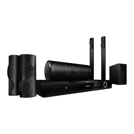
DVD Home Theater System
Service
Service Manual
©
Copyright 2010 Philips Consumer Electronics B.V. Eindhoven, The Netherlands
All rights reserved. No part of this publication may be reproduced, stored in a retrieval system or
transmitted, in any form or by any means, electronic, mechanical, photocopying, or otherwise
without the prior permission of Philips.
Published by
RY1003
Service Audio Printed in The Netherlands Subject to modification
Version 1.1
TABLE OF CONTENTS
Location of PCB Boards ............................................ 1-2
Versions Variation ...................................................... 1-2
Specifications ............................................................ 1-3
Measurement Setup .................................................. 1-4
Service Aids .............................................................. 1-5
ESD & Safety Instruction .......................................... 1-6
Lead-free soldering Information ................................ 1-7
Setting procedure & Repair Instructions........................ 2
Disassembly Instructions & Service positions .............. 3
Block & Wiring Diagram ................................................ 4
VFD Board .................................................................... 5
Main Board .................................................................... 6
Power Board .................................................................. 7
AMP Board .................................................................... 8
Scart Board .................................................................... 9
VOL+USB+MP3 Board ................................................ 10
Touch Board ................................................................ 11
Jack Board .................................................................. 12
Mechanical Exploded view .......................................... 13
Revision List ................................................................ 14
1 - 1
Chapter
HTS5540
/12/05
HTS5550
/12
3139 785 35200
GB
Advertisement

Related Manuals for Philips HTS5540


Summary of Contents for Philips HTS5540
- Page 1 Revision List ..............14 © Copyright 2010 Philips Consumer Electronics B.V. Eindhoven, The Netherlands All rights reserved. No part of this publication may be reproduced, stored in a retrieval system or transmitted, in any form or by any means, electronic, mechanical, photocopying, or otherwise without the prior permission of Philips.
- Page 2 JACK PCB MAIN PCB AMP PCB TOUCH PCB POWER PCB VFD PCB VOL PCB MP3 PCB USB PCB VERSION VARIATION: Type/Versions HTS5540 HTS5550 Features Output Power - 1200W Voltage (220~240V) Scart SERVICE SCNARIO MATRIX: HTS5540 HTS5550 Type/Versions Board in used...
- Page 3 1 - 3 SPECIFICATIONS Playback media Dimensions (WxHxD): Center ............280 x 95 x 92 (mm) DVD-Video, DVD+R/+RW, DVD-R/-RW, DVD+RDL, CD-R/CD- Speaker ..........100 x 280 x 115 (mm) RW, Audio CD, Video CD/SVCD,Picture CD, MP3-CD, WMA- Tall speaker .......... 260 x 1101 x 260 (mm) CD, DivX-CD, USB storage device Weight: Center ................
- Page 4 1 - 4 MEASUREMENT SETUP Tuner FM Bandpass LF Voltmeter 250Hz-15kHz e.g. PM2534 e.g. 7122 707 48001 RF Generator e.g. PM5326 S/N and distortion meter e.g. Sound Technology ST1700B Use a bandpass filter to eliminate hum (50Hz, 100Hz) and disturbance from the pilottone (19kHz, 38kHz). Use Audio Signal Disc SBC429 4822 397 30184 (replaces test disc 3)
- Page 5 1 - 5 SERVICE AIDS Service Tools: Universal Torx driver holder .........4822 395 91019 Torx bit T10 150mm ...........4822 395 50456 Torx driver set T6-T20 .........4822 395 50145 Torx driver T10 extended ........4822 395 50423 Compact Disc: SBC426/426A Test disc 5 + 5A ......4822 397 30096 SBC442 Audio Burn-in test disc 1kHz ....4822 397 30155 SBC429 Audio Signals disc .........4822 397 30184 Dolby Pro-logic Test Disc ........4822 395 10216...
- Page 6 1 - 5 WAARSCHUWING WARNING Alle IC’s en vele andere halfgeleiders zijn All ICs and many other semi-conductors are gevoelig voor electrostatische ontladingen susceptible to electrostatic discharges (ESD). (ESD). Careless handling during repair can reduce life Onzorgvuldig behandelen tijdens reparatie kan drastically.
- Page 7 Due to lead-free technology some rules have to be Philips-sets respected by the workshop during a repair: You will find this and more technical information Use only lead-free solder alloy Philips SAC305 with • within the “magazine”, chapter “workshop news”. order code 0622 149 00106. If lead-free solder-paste...
- Page 8 2 - 1 2 - 1 System , Region Code , etc. Setting Produre 1)Restore factory setting 6) Upgrading new software a) Press <SETUP> button on R/C a) Copy the latest upgrading software onto a CD-R or USB storage b) Select <preference setup> ,then press < OK > device c) Select <default>,then press <OK>...
- Page 9 2 - 2 2 - 2 REPAIR INSTRUCTIONS (One)
- Page 10 2 - 3 2 - 3 REPAIR INSTRUCTIONS (Two)
- Page 11 2 - 4 2 - 4 REPAIR INSTRUCTIONS (Three)
- Page 12 3 - 1 3 - 1 DISASSEMBLY INSTRUCTIONS Dismantling of theTop & Front Panel Assemble 3) Loosen 6 screws and remove the Top Cover by lifting the rear portion upwards before sliding it out towards the rear. - 4 screws “A” at the back panel as shown in gure 4. 1) Open the DVD Tray by using the Open/Close Button while the Set is ON and disconnect the mains supply after removing the Tray - 1 screw “B”...
- Page 13 3 - 2 3 - 2 Dismantling of the VFD Board Dismantling of the POWER Board 1) Loosen 3 screws “G” on the top of VFD Board as shown in gure 10. 1) Loosen 5 screws “K” on the top of power Board as shown in gure 14. Figure 10 Dismantling of the VOL+USB+MP3 Board and VOL Button 1) Loosen 7 screws “H”...
- Page 14 3 - 3 3 - 3 Dismantling of the SCART Board 1) Loosen 2 screws “O” at the back panel as shown in gure 17. Figure 17 Dismantling of the JACK Board 1) Loosen 2 screws “P” on the top of JACK board as shown in gure 18. Figure 18 Dismantling of the TOUCH Board 1) Loosen 3 screws “Q”...
- Page 15 4 - 1 4 - 1 BLOCK DIAGRAM...
- Page 16 4 - 2 4 - 2 WIRING DIAGRAM JACK PCB AMP PCB MAIN PCB POWER PCB VFD PCB TOUCH PCB...
- Page 17 5 - 1 5 - 1 FTD DISPLAY PIN ASSIGNMENT VFD BOARD TABLE OF CONTENTS FTD Display Pin Assignment ............. 5-1 Circuit Diagram ................. 5-2 PCB Layout Top & Bottom View ............5-3 PIN CONNECTION...
- Page 18 5 - 2 5 - 2 CIRCUIT DIAGRAM C392 ZD312 A1 C391 DP351 A3 C381 C385 Q352 R3052 B1 R3055 B1 R3058 B1 RB357 B1 C389 R3060 B2 R3061 A1 C387 R3067 A2 R3068 A3 C382 C386 Q352 R3053 B1 R3056 B1 R3059 B1 SN351 B1...
- Page 19 5 - 3 5 - 3 PCB LAYOUT - TOP VIEW C386 C391 CN360 A1 R3061 A1 RB356 A1 SN351 A1 DP351 A3 C389 C392 RB355 A1 RB357 A1 ESD1 A1 ESD2 A3 PCB LAYOUT - BOTTOM VIEW C385 Q352 A1 R3058 A1 R3060 A1 ZD311 A1...
- Page 20 6 - 1 6 - 1 INTERNAL IC DIAGRAM - MT1389FEX/SN DVB-T HDMI1.2Tx RGB video Module CVBS MT1389S MAIN BOARD FLASH 8ch Audio SPDIF Front-panel USB2.0/3 in 1 card DRAM Remote reader TABLE OF CONTENTS Internal IC Diagram ................6-1 Circuit Diagram(part one) ..............
- Page 21 6 - 2 6 - 2 CIRCUIT DIAGRAM - part one C801 A1 R820 A1 C802 A2 IC205 A2 C0207 A3 C721 A3 L707 R734 A3 Q720 A4 C227 B1 FB803 B1 C228 B2 C840 B2 RA203 B2 CN206 B4 C0217 C1 C257 C1 CE809 C1...
- Page 22 6 - 3 6 - 3 CIRCUIT DIAGRAM - part two C1213 A1 R1222 A1 R1235 A1 C334 R332 C340 R389 R506 R522 C355 FB905 B1 R368 C320 R307 C512 FB304 B4 R3028 B4 C919 CE307 C1 CE322 C1 FE306 C1 R929 C1214 A1 R1223 A1...
- Page 23 6 - 4 6 - 4 PCB LAYOUT - TOP VIEW C1203 A1 Q703 A1 R739 A1 JK703 A2 C352 A3 R306 A3 R1223 A4 C1210 B1 R1203 B1 C237 B2 C0235 B3 FB208 B3 R353 B3 R226 B4 C201 C1 L202 R826 C1 CN202 C2...
- Page 24 6 - 5 6 - 5 PCB LAYOUT - BOTTOM VIEW C1200 A1 C0222 A2 FE306 A2 C1217 A3 C371 C1223 B1 FB713 B1 C0215 B2 C0228 B2 C0601 B2 C837 FE307 B2 C315 C324 R538 CE205 C2 CE804 C2 C233 CE207 C3 C509...
- Page 25 7 - 1 7 - 1 INTERNAL IC DIAGRAM - AZ431 CATHODE POWER BOARD ANODE TABLE OF CONTENTS Internal IC Diagram ................7-1 Circuit Diagram .................. 7-2 PCB Layout Top View ............... 7-3 PCB Layout Bottom View ..............7-4 INTERNAL IC DIAGRAM - AZ7500BP OUTPUT CTRL Oscillator Pulse-Steering...
- Page 26 7 - 2 7 - 2 CIRCUIT DIAGRAM BD901 A1 TVR903 A1 R949 C970 L908 R976 R953 C918 R906 D903 R943 C930 D923 R922 R995 Q922 C903 J906 IC904 R986 R936 C904 C910 R950 C971 R908 ZD908 A3 R954 C919 R910 D905 R990...
- Page 27 7 - 3 7 - 3 PCB LAYOUT - TOP VIEW BD901 A1 C939 R914 C944 J906 C931 Q925 J911 C918 C909 R941 C913 GT903 B3 T902 D912 J919 ZD910 B4 C902 L908 C904 C942 R933 C946 J908 C933 R928 J913 GT902 B1 D902...
- Page 28 7 - 4 7 - 4 PCB LAYOUT - BOTTOM VIEW R917 A1 C921 A3 C989 A3 R947 A3 C985 A4 Q922 A4 R930 A4 R993 A4 D906 B2 C964 B4 C988 B4 R956 B4 R976 B4 ZD907 B4 R906 C1 C958 C4 R955 C4 R918 A1...
- Page 29 8 - 1 8 - 1 INTERNAL IC DIAGRAM - TA5508APAG AMP BOARD TABLE OF CONTENTS Internal IC Diagram ................8-1 INTERNAL IC DIAGRAM - TAS5352 2ADDV Circuit Diagram .................. 8-2 PCB Layout Top & Bottom View ............8-3 System Microcontroller BST_A Bootstrap...
- Page 30 8 - 2 8 - 2 CIRCUIT DIAGRAM C5001 R5001 R5006 C5184 R5171 C5142 R5012 R5180 C5072 R5049 C5054 R5095 C5082 R5106 C5112 R5069 C5047 C5541 R5137 C5155 R5116 Q5005 C3 R5195 R5155 C5002 R5002 R5007 C5185 R5172 C5148 R5021 R5181 C5073 R5056...
- Page 31 8 - 3 8 - 3 PCB LAYOUT - TOP VIEW C5068 Q5005 B1 C5084 R5061 C5042 C5173 Q5006 B1 C5085 R5082 C5043 C5177 R5021 C5086 R5094 C5044 D5005 R5022 C5088 R5097 C5053 IC5007 A1 R5023 C5090 R5102 C5063 Q5007 A1 R5024 C5092 R5103...
- Page 32 8 - 4 8 - 4 PCB LAYOUT - BOTTOM VIEW FB5001 A1 R5160 R5220 R5187 R5221 R5195 C5166 ZD5001 C1 C5185 ZD5002 C1 C5186 C5105 C5187 R5009 C5190 C5001 C5191 C5005 D5007 C5006 R5146 C5008 R5147 C5009 R5149 C5010 R5151 C5087 R5175...
- Page 33 9 - 1 9 - 1 SCART BOARD TABLE OF CONTENTS Circuit Diagram ................. 9-2 PCB Layout Scart PCB View ............. 9-3...
- Page 34 9 - 2 9 - 2 CIRCUIT DIAGRAM C710 C712 C714 FB707 B1 FB709 B1 FB711 A2 JK703 A2 R708 RB702 A1 C711 C713 C715 FB708 B1 FB710 A2 FB714 C2 R707 RB701 B1...
- Page 35 9 - 3 9 - 3 PCB LAYOUT - SCART PCB VIEW C710 C712 C714 FB707 A2 FB709 B3 FB711 A1 JK703 A2 R708 RB702 B1 C711 C713 C715 FB708 A1 FB710 A1 FB714 A1 R707 RB701 B3...
- Page 36 10 - 1 10 - 1 VOL+USB+MP3 BOARD TABLE OF CONTENTS Circuit Diagram .................. 10-2 PCB Layout Top View ............... 10-3 PCB Layout Bottom View ..............10-4...
- Page 37 10 - 2 10 - 2 CIRCUIT DIAGRAM RB17 RB15 FB11 FB16 JK11 VR11 USB11 A3 FB12 FB17 RB357 B1...
- Page 38 10 - 3 10 - 3 PCB LAYOUT - TOP VIEW JK11 RB357 A1 JW20 JW21 USB11 A2 RB15 RB17 VR11...
- Page 39 10 - 4 10 - 4 PCB LAYOUT - BOTTOM VIEW FB11 A1 FB12 A1 FB16 A1 FB17 A1...
- Page 40 11 - 1 11 - 1 TOUCH BOARD TABLE OF CONTENTS Circuit Diagram .................. 11-2 PCB Layout Top View & Bottom View ..........11-3...
- Page 41 11 - 2 11 - 2 CIRCUIT DIAGRAM...
- Page 42 11 - 3 11 - 3 PCB LAYOUT - TOP & BOTTOM VIEW RB360 A3...
- Page 43 12 - 1 12 - 1 JACK BOARD TABLE OF CONTENTS Circuit Diagram .................. 12-2 PCB Layout Top View & Bottom View ..........12-3...
- Page 44 12 - 2 12 - 2 CIRCUIT DIAGRAM CN103 A1 JK102 Q104 Q105 Q106 Q107 Q108...
- Page 45 12 - 3 12 - 3 PCB LAYOUT - TOP & BOTTOM VIEW CN103 A1 JK102 Q104 Q105 Q106 Q107 Q108...
- Page 46 13 - 1 13 - 1 Mechanical Exploded View HDMI...
- Page 47 14 - 1 14 - 1 REVISION LIST Version 1.0 *Initial release Version 1.1 *hts5540/12/05 /hts5550/12 combine...