Table of Contents
Advertisement
SY
011825
20060525-147000
SERVICE MANUAL
CONTENTS (目次)
SPECIFICATIONS (総合仕様) ................................................... 3
Panel Layout (パネルレイアウト)...................................... 4
Disassembly Procedure (分解手順)............................... 7
LSI PIN DESCRIPTION (LSI端子機能表)............................... 13
IC BLOCK DIAGRAM (ICブロック図) .................................... 16
CIRCUIT BOARDS (シート基板図)........................................ 16
TEST PROGRAM (テストプログラム) .............................. 26/33
BULK DUMP(BACKING UP THE DATA)
(バルクダンプ (データのバックアップ) ) ........................ 40/43
FACTORY PRESET RECALL ( 初期設定に戻すには) ......... 46/48
MESSAGE LIST (メッセージ一覧) ......................................... 50
(起動フローチャート) ..................................................... 51/52
Midi Implementation Chart (Voice) ........................... 53
Midi Implementation Chart (Master) ....................... 54
Midi Data Format ............................................................. 55
BLOCK DIAGRAM (ブロックダイアグラム)
CIRCUIT BOARD LAYOUT & WIRING
(ユニットレイアウト&結線図)
OVERALL CIRCUIT DIAGRAM (総回路図)
Copyright (c) Yamaha Corporation. All rights reserved. PDF M
I
'06.05
Advertisement
Table of Contents

Related Manuals for Yamaha CP33


Summary of Contents for Yamaha CP33
- Page 1 MIDI IMPLEMENTATION CHART (VOICE) ......53 MIDI IMPLEMENTATION CHART (MASTER) ....... 54 MIDI DATA FORMAT ............. 55 PARTS LIST BLOCK DIAGRAM (ブロックダイアグラム) CIRCUIT BOARD LAYOUT & WIRING (ユニットレイアウト&結線図) OVERALL CIRCUIT DIAGRAM (総回路図) 011825 20060525-147000 Copyright (c) Yamaha Corporation. All rights reserved. PDF M ’06.05...
- Page 2 CP33 IMPORTANT NOTICE This manual has been provided for the use of authorized Yamaha Retailers and their service personnel. It has been assumed that basic service procedures inherent to the industry, and more specifically Yamaha Products, are already known and understood by the users, and have therefore not been restated.
- Page 3 Dimensions (W x D x H) 1312 x 330 x 151 mm (51-2/3" x 13 x 5-15/16") Weight 18 kg (39 lbs., 11 oz) Accessories Owner’s Manual, Foot Pedal FC3, Yamaha PA-3C power adaptor ■ 総合仕様 項目 内容 鍵盤 GH 鍵盤 88 鍵...
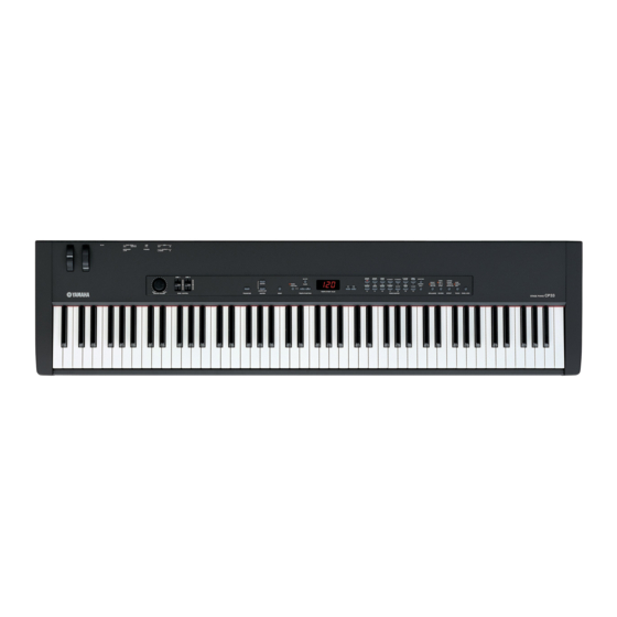
- Page 4 CP33 PANEL LAYOUT(パネルレイアウト) Front Panel (フロントパネル) FOOT PEDAL MIDI DC-IN SUSTAIN STANDBY PHONES OUTPUT L/MONO ZONE 1 ZONE 2 ON/OFF MASTER TEMPO CLICK FUNCTION MASTER EDIT TEMPO/OTHER MASTER VOLUME ZONE CONTROL TRANSPOSE MASTER DEMO TEMPO/FUNCTION 1 Pitch bend wheel 1 ピ ッ チベン ドホイ ール...
- Page 5 CP33 & * GRAND GRAND MONO E. CLAVI- VIBRA- VARIATION PIANO 1 PIANO 2 PIANO E. PIANO 1 E. PIANO 2 CHORD PHONE ROOM CHORUS BRIGHT HALL 1 PHASER HARD MEMORY NORMAL HALL 2 TREMOLO MEDIUM CHURCH JAZZ HARPSI- STRINGS/...
- Page 6 CP33 Rear Panel (リアパネル) DC-IN OUTPUT PHONES STANDBY L/MONO MIDI FOOT PEDAL SUSTAIN 1 OUTPUT [L/MONO][R] jacks 1 OUTPUT (アウ トプッ ト) [L/MONO][R] 端子 2 MIDI [IN][OUT] connectors 2 MIDI (ミ ディ) [IN (イ ン) ] [OUT (アウ ト) ]端子 3 [PHONES] jack 3 [PHONES] (フォ...
- Page 7 CP33 DISASSEMBLY PROCEDURE(分解手順) 上ケースAss y Upper Case Assembly (所要時間 : 約2分) 棚板下より[50] のネジ5本と[60] のネジ6本を外し (Time required: About 2 minutes) て、 上ケースAss yを後方にスライドした後、 持ち上 Remove the five (5) screws marked [50] and the six げて外します。 ( 図1) (6) screws marked [60] located under the keybed. Move the upper case assembly rearward, and it can then be remove by lifting up.
- Page 8 CP33 Upper Case Assembly (上ケースAss y) ● Wheel assembly (MODULATION) [410E] [410D] [410B] [410B] [410B] [410C] [410C] [270B] [270C] [410A] [410A] Wheel assembly AJACK (PITCH BEND) DJACK [420] [270A] [270A] AJACK DJACK [330A] [320] [330B] Fig. 2 (図2) Keyboard Assembly GHD EBUS鍵盤 ...
- Page 9 CP33 Side Cover Assembly (L, R) 腕木Ass y (L ・ R) (所要時間 : 約4分) (Time required: About 4 minutes) 上ケースAss yを外します。 ( 1項参照) Remove the upper case assembly. (See procedure 1) [270D]のネジ5本を外し、 腕木Ass y (R)を外します。 Remove the five (5) screws marked [270D]. The side (図4)...
- Page 10 CP33 GHD EBUS L, MK SUB Circuit Board GHD EBUS L, MK SUBシート (所要時間 : 約7分) 6 ‐ 1 (Time required: About 7 minutes) [260A]のネジ7本を外し、 GHD EBUS L, MK SUB Remove the seven (7) screws marked [260A]. The シートを外します。 ( 図7、 7-1) GHD EBUS L and MK SUB circuit boards can then 6 ‐...
- Page 11 CP33 White key 6 ‐ 5 白鍵 In order to release the white key from the stopper, insert 白鍵をストッパーから外すために、 薄い金尺状のも a thin plate between the white keys (gap in the direction のを鍵盤の間に挿入して (三角マークの示す方向側 indicated by the triangle mark, near the fulcrum of the の隙...
- Page 12 CP33 Spring スプリング Place the keyboard assembly right side up. Fix key GHD EBUS鍵盤を表側にして、 端が二本に分かれて springs on the frame by setting one at each slit and いるスプリングの先をハンマー白鍵 (黒鍵) の切り込 pushing down once on each key spring. (Fig. 15) みに合わせて、 一度下に押し込んでフレームのフッ Be careful of the direction of the spring. It should be クに取り付けます。...
- Page 13 CP33 LSI PIN DESCRIPTION(LSI 端子機能表) AK4385ET (X6040A00) DAC (Digital to Analog Converter) ....... . 13 HD6433690B70FYV (X6008200) CPU (E-HOSTs) .
- Page 14 CP33 YMW767-VTZ (X6055A00) CPU (SWL01B) DM: IC004, 007 NAME FUNCTION NAME FUNCTION Ground Ground Input for TEST Power supply +3.3 V TESTN PLLBPN PLL bypass select External memory lower-byte enable / Port F LBN/LWRN/PF6 PLLV PLL Power supply +2.5 V...
- Page 15 CP33 HD6433690B70FYV (X6008200) CPU (E-HOSTs) DM: IC024 NAME FUNCTION FUNCTION NAME Avcc Analog Power Supply (+3.3V) (Pull Up) /NMI Sub Clock Output - (NC) Sub Clock Input - (NC) Internal Power Supply (+3.3V) - (NC) /RES RESET input - (NC)
- Page 16 CP33 IC BLOCK DIAGRAM(IC ブロック図) TC74VHCT245AFT (XT744B00) SN74LV32APWR (X5647A00) SN74LV126APWR (X3865A00) Octal 3-State Bus Transceiver Quad 2 Input OR Bus Buffer DM: IC028 DM: IC018 DM: IC029 µPC4572G2-E1-A (X7433A00) TC7S08FU (XP116A00) µPC4570G2-E1-A (X7351A00) 2 Input AND Gate Dual Operational Amplifier...
- Page 17 CP33 DM Circuit Board not installed to GHD EBUS L-CN1 to PNL-CN301 to DJACK-CN601 to SVR-CN802 (to PNR-CN302) Component side (部品側) to DJACK-CN701 to PNL-CN201 to PNL-CN101 to AJACK-CN101 (to PNR-CN202) (to PNR-CN102) Pattern side (パターン側) 2NA-WD97020-1 2NA-WD97020-2...
- Page 18 CP33 AJACK Circuit Board Pattern side Component side (パターン側) (部品側) 2NA-WG40060...
- Page 19 CP33 DJACK Circuit Board FOOT PEDAL MIDI SUSTAIN Component side to DM-CN3 to DM-CN9 to DM-CN2 (部品側) Pattern side (パターン側) MVR Circuit Board to AJACK-CN302 Pattern side Component side (パターン側) (部品側) MASTER VOLUME DJACK, MVR: 2NA-WG40060...
- Page 20 CP33 PNL Circuit Board to PNR-CN302 to PNR-CN202 to DM-CN4 to DM-CN5 MASTER TRANSPOSE MASTER EDIT DEMO to PNR-CN102 to DM-CN6 CLICK ON/OFF TEMPO/OTHER VALUE TEMPO FUNCTION TEMPO/ TEMPO/ FUNCTION – FUNCTION + TEMPO/ FUNCTION YES/+ NO/ – Component side (部品側)...
- Page 21 CP33 PNR Circuit Board to PNL-CN301 to PNL-CN201 (to DM-CN4) (to DM-CN5) GRAND GRAND MONO VIBRA- E. CLAVI- VARIATION BRIGHT E. PIANO 1/4 E. PIANO 2/5 PHONE/7 PIANO 1/1 PIANO 2/2 CHORD/6 PIANO/3 NORMAL MELLOW STRINGS/ JAZZ HARPSI- WOOD CHURCH E.
- Page 22 CP33 SVR Circuit Board to DM-CN10 (to GHD EBUS L-CN1) to WHEEL Assembly ZONE 1 ZONE 2 Component side ZONE CONTROL (部品側) Pattern side (パターン側) MK SUB Circuit Board not installed Pattern side Component side (パターン側) (部品側) to GHD EBUS L-CN5...
- Page 23 CP33 GHD EBUS L Circuit Board 2NAK8-V646930...
- Page 24 CP33 GHD M Circuit Board 2NAK8-V852140...
- Page 25 CP33 GHD H Circuit Board 2NAK8-V852150...
- Page 26 Method 2) While pressing the [VOICE 1], [VOICE 3] and [VOICE 5] buttons simultaneously, turn on the [STANDBY/ON] switch. Method 3) Send the MIDI code “F0 43 73 01 60 00 F7” to CP33 to enter the TEST mode. (See page 31) PROCEEDING THROUGH THE TEST PROGRAM 1) Once inside the test program, the 7-seg.
- Page 27 CP33 Test Items Test No. 7-seg. LED display Test Functions and Judgment Criteria Selected screen ROM version display When OK A*. * Checks that the 7-seg. LED displays the ROM (Master, Slave) versions alternately. ← → b*. * A*. *...
- Page 28 CP33 Test No. 7-seg. LED for Each Test Test Functions and Judgment Criteria Selected screen EQ Low frequency check (outputs about 65.4Hz (C1) sine wave tone) Test in progress For factory test use only. Check completed Sound production stops when returning to selection screen with the [CLICK ON/OFF] button.
- Page 29 CP33 Test No. 7-seg. LED for Each Test Test Functions and Judgment Criteria Selected screen Zone slider 1 check Test in progress Before starting the test, set the ZONE CONTROL [ZONE1] slider at the center position. ↓ Execute the test. When the [ZONE1] slider is set forward (Min), the C3 tone sounds, when it is set to the other side (Max), the G3 tone sounds and when it is set to the center position ↓...
- Page 30 CP33 Test No. 7-seg. LED for Each Test Test Functions and Judgment Criteria Selected screen Master ROM check 2 Test in progress For factory test use only. When OK It takes about 30 seconds before checking is completed. When NG Check completed (.
- Page 31 CP33 TEST PROGRAM using MIDI code To select the item after testing, send “A2, 00, 00” and then the MIDI code of the test item. Test No. Test Item MIDI Cord MIDI OUT Version A0, 01, 00 F0, 43, 73, 01, 68, 00, 00, 00, 00, F7 : START F0, 43, 73, 01, 68, 01, V1, V2, V3, F7 : Master Wave1 F0, 43, 73, 01, 68, 02, V1, V2, V3, F7 : Slave Wave2 F0, 43, 73, 01, 68, 00, 00, 00, 7F, F7 : < V1, V2, V3 > Version Number (ASCII code) Master ROM Check1...
- Page 32 CP33 Test No. Test Item MIDI Cord MIDI OUT Mod Wheel Check A0, 1E, 00 A1, 1E, 00 : Item change A0, 1E, 02 : OK Zone Slider 1 Check A0, 1F, 00 A1, 1F, 00 : Item change A0, 1F, 02 : OK Zone Slider 2 Check A0, 20, 00 A1, 20, 00 : Item change A0, 20, 02 : OK MIDI Check Check in the manual mode USB Check Check in the manual mode Keyboard TYPE Check A0, 25, 00 A1, 25, 00 : Item change A0, 25, 02 : OK ( A0, 25, 03 :NG ) Master ROM Check2 A0, 2B, 00 A1, 2B, 00 : Item change A0, 2B, 02 : OK ( A0, 2B, 03 :NG ) Slave ROM Check2 A0, 2C, 00 A1, 2C, 00 : Item change A0, 2C, 02 : OK ( A0, 2C, 03 :NG ) RAM Check2 A0, 2D, 00 A1, 2D, 00 : Item change A0, 2D, 02 : OK ( A0, 2D, 03 :NG ) Flash ROM Check2 A0, 2F, 00 A1, 2F, 00 : Item change A0, 2F, 02 : OK ( A0, 2F, 03 :NG )...
- Page 33 4 ) PCとCP33を接続する為にはUSB-MIDIドライバーをインストールする必要があります。 USB-MIDIドライバーは下記のURLからダウンロードしてください。 http://www.yamaha.co.jp/download/usb̲midi/ 5)Factory Set (テストNo.49) またはFlash ROM check 2 ( テストNo.47) を行うとユーザのデータが消去されます。 事前にデータバックアップを行ってください。 ( 43ページ参照) テストプログラムの起動 方法1) [C#2] と[F2] と[G#2] の鍵盤を同時に押さえながら、 [STANDBY/ON] スイッチをON にします。 方法2) ボイスボタンの[VOICE 1]と[VOICE 3]と[VOICE 5]を押しながら、 [STANDBY/ON] スイッチをON にします。 方法3) CP33にMIDIコード F0 43 73 01 60 00 F7 を送るとテストモードに入ります。 ( 38ページ参照) テストの進め方 1) テストプログラムが起動されると、 7 セグメントLED に と表示されます。 2) [TEMPO/FUNCTION]の[ + ]、 [ − ] ボタンを押して、 テストナンバーを選択します。 3) [CLICK ON/OFF] ボタンを押して、 テストを実行します。 テストの結果がOK の場合は、 7 セグメントLED に と表示されます。...
- Page 34 CP33 テスト一覧 テスト No. LED (7-seg.) 表示 テスト内容および判定条件など ROM のバージ ョ ン表示 選択画面 LED (7-seg.)に ROM (Master,Slave)のバージ ョ ンが交互に表示される こ と を確認します。 A*. * OKの場合 ← → b*. * A*. * b*. * (A: Master 側 ROM, b: Slave 側 ROM, *. * : ROMのバージョン NGの場合 (. 0 . 1 .
- Page 35 CP33 テスト No. LED (7-seg.) 表示 テスト内容および判定条件など EQ Mid 周波数チェ ッ ク(約 523Hz (C4) の正弦波を出力します。 ) 選択画面 工場検査用のテス ト です。 テスト中 [CLICK ON/OFF]ボ タ ン を押して選択画面に戻る際、発音が止ま り ます。 (. 1 . 5 . チェック終了 EQ High 周波数チェ ッ ク(約 4186Hz (C7) の正弦波を出力し ます。 ) 選択画面 工場検査用のテス ト です。 テスト中 [CLICK ON/OFF]ボ タ ン を押して選択画面に戻る際、発音が止ま り ます。...
- Page 36 CP33 テスト No. LED (7-seg.) 表示 テスト内容および判定条件など ゾーン ス ラ イ ダー 1 チェ ッ ク 選択画面 テス ト に入る前に、ZONE CONTROL の[ZONE 1]ス ラ イ ダーを中央(セン タ ー)に しておき テスト中 ↓ ます。 テス ト を実行し、 [ZONE 1]ス ラ イ ダーを手前(Min)にする とC3 を発音し、奥(Max)に ↓ する とG3 を発音し、再び中央(セン タ ー)にする とC3 を発音します。...
- Page 37 CP33 テスト No. LED (7-seg.) 表示 テスト内容および判定条件など Master ROM チェ ッ ク2 選択画面 工場検査用のテス ト です。 テスト中 チェ ッ ク完了まで約 30 秒かかり ます。 OKの場合 NGの場合 (. 4 . 3 . チェック終了 Slave ROM チェ ッ ク2 選択画面 工場検査用のテス ト です。 テスト中 チェ ッ ク完了まで約 50 秒かかり ます。...
- Page 38 CP33 MIDIコードでのテストプログラム テスト後、 項目選択にするには A2, 00, 00 を送ってからテスト項目のMIDIコードを送ってください。 テスト No. テスト項目 MIDI コード MIDI 出力 Version A0, 01, 00 F0, 43, 73, 01, 68, 00, 00, 00, 00, F7 : START F0, 43, 73, 01, 68, 01, V1, V2, V3, F7 : Master Wave1 F0, 43, 73, 01, 68, 02, V1, V2, V3, F7 : Slave Wave2 F0, 43, 73, 01, 68, 00, 00, 00, 7F, F7 : < V1, V2, V3 > Version Number (ASCII code) Master ROM Check1 A0, 02, 00 A1, 02, 00 : Item change A0, 02, 02 : OK ( A0, 02, 03 :NG ) Slave ROM Check1 A0, 03, 00 A1, 03, 00 : Item change A0, 03, 02 : OK ( A0, 03, 03 :NG ) RAM Check1 A0, 04, 00 A1, 04, 00 : Item change A0, 04, 02 : OK ( A0, 04, 03 :NG ) Flash ROM Check1 A0, 05, 00 A1, 05, 00 : Item change A0, 05, 02 : OK ( A0, 05, 03 :NG )...
- Page 39 CP33 テスト No. テスト項目 MIDI コード MIDI 出力 Mod Wheel Check A0, 1E, 00 A1, 1E, 00 : Item change A0, 1E, 02 : OK Zone Slider 1 Check A0, 1F, 00 A1, 1F, 00 : Item change A0, 1F, 02 : OK Zone Slider 2 Check A0, 20, 00 A1, 20, 00 : Item change A0, 20, 02 : OK MIDI Check manual mode でチェック USB Check manual mode でチェック Keyboard TYPE Check A0, 25, 00 A1, 25, 00 : Item change A0, 25, 02 : OK ( A0, 25, 03 :NG ) Master ROM Check2 A0, 2B, 00 A1, 2B, 00 : Item change A0, 2B, 02 : OK ( A0, 2B, 03 :NG ) Slave ROM Check2 A0, 2C, 00 A1, 2C, 00 : Item change A0, 2C, 02 : OK ( A0, 2C, 03 :NG ) RAM Check2 A0, 2D, 00 A1, 2D, 00 : Item change A0, 2D, 02 : OK ( A0, 2D, 03 :NG )...
- Page 40 BULK DUMP (BACKING UP THE DATA) It is possible to back up the data by sending the following System Exclusive Message (Bulk Request) to CP33. (Note that it is possible to back up only setting data of the master function and not the function data.) MIDI DATA: ...
- Page 41 3) Open bulk-out template "cp33-bulk.mid" of SQ01. (In the general setting conditions, it can be opened by double clicking "cp33-bulk.mid".) 4) Select Set up, MIDI and Device in that order. Select [YAMAHA USB IN 0-1] for Input and [YAMAHA USB OUT 0-1] for Output and click...
- Page 42 6) Save the data by another name. (Writing over will damage the template.) Any format can be used but SMF format 1 is recommended. 7) To return the data to CP33, open the data saved by another name and click PLAY --- ".
- Page 43 CP33 ■ バルクダンプ (データのバックアップ) CP33に下記のSystem Exculusive Message(Bulk Request)を送ればデータをバックアップすることができます。 (マスター機能の設定のみバックアップが可能です。ファンクションはバックアップできませんので注意してください。) MIDI DATA: F 0 43 20 7F 05 33 00 00 F7 F0: Exclusive Status 43: Yamaha ID 20: When received 7F: CP33 ID High 05: CP33 ID Low 33: Master Setting Address High 00: Master Setting Address Mid 00: Master Setting Address Low F7: End of Exclusive ここでは、MIDI/オーディオシーケンスソフトウエア "SQ01" とバルクアウトのテンプレート(cp33̲bulk.mid) を使用 した場合を例として説明します。(SQ01はインストールされているものとします。) CP33とコンピューターの接続 USBケーブル(A-Bタイプ) USB端子 USB端子 ZONE 1 ZONE 2 GRAND GRAND MONO E.
- Page 44 CP33 3) SQ01でのバルクアウトテンプレート "cp33̲bulk.mid" を開きます。 (一般的な設定状態では、"cp33̲bulk.mid " をダブルクリックすれば開きます。) 4) 設定→MIDI→デバイスを選択します。 入力に[YAMAHA USB IN 0-1]、出力に[YAMAHA USB OUT 0-1]を選択して、 をクリックします。...
- Page 45 CP33 5) REC → PLAY をクリックすればデータのバックアップが開始されます。 スタートすればカーソルが動きます。 バルクデータが出力され、Block のサイズが変化します。 Block1 の部分すべてが完了(カーソルが通過)すれば STOP をクリックします。 (もう一度 STOP をクリックすればカーソルはスタート位置(起点)に戻ります。) 6) 取り出したデータを別名で保存してください。(上書きするとテンプレートが壊れます。) 推奨は SMF format1 形式ですがどの形式でも使用可能です。 7) CP33にデータを戻すには、別名保存したデータを開いて PLAY をクリックします。 作業中はCP33の7セグメントLEDに が表示されます。 (この間は、CP33の電源を切らないように注意してください。) 完了すれば 7セグメントLEDに が表示されます。 ...
- Page 46 CP33 FACTORY PRESET RECALL All settings affected by the Functions (F1 – F8) can be restored to their original factory preset values by turning the [STANDBY/ON] STANDBY ROOM CHORUS switch ON while holding the rightmost white key (C7) and black keys...
- Page 47 CP33 Function Settings Display Function Default Backup Group Tuning A3 = 440Hz F2.1 Scale 1 (Equal Temperament) F8.3 F2.2 Base Note F3.1 Dual Detune Preset for each Voice combination F3.2, F3.3 Dual Octave Shift Preset for each Voice combination F3.4, F3.5...
- Page 48 CP33 初期設定に戻すには いったん電源をオフにし、 右端の鍵盤(C7)と黒鍵(F#6、 G#6、 A#6)を 押したまま電源をオンにします。 STANDBY ROOM CHORUS BRIGHT HALL 1 PHASER HARD NORMAL HALL 2 TREMOLO MEDIUM MELLOW STAGE ROTARY SP SOFT この操作で、 ファンクションのF1からF8のすべての項目が初期設定 PANEL BRILLIANCE REVERB EFFECT TOUCH LOCK FOOT PEDAL (=工場出荷時の状態)に戻ります。 SUSTAIN 楽器の画面に 「CLr」 が表示されます。 この表示が出ている間は、 電...
- Page 49 CP33 ファンクションの初期設定一覧 バックアップ 表示 項目 初期設定 グループ 音の高さ A3=440Hz F2.1 音律 1(平均律) F8.3 F2.2 基音 F3.1 2ボイスの音の高さ ボイスの組み合わせごと F3.2 第1ボイスのオクターブシフト ボイスの組み合わせごと F3.3 第2ボイスのオクターブシフト ボイスの組み合わせごと F3.4 第1ボイスのエフェクトの深さ ボイスの組み合わせごと F3.5 第2ボイスのエフェクトの深さ ボイスの組み合わせごと F4.1 スプリットポイント F #2 F8.1 F4.2 右側ボイスのオクターブシフト ボイスの組み合わせごと F4.3 左側ボイスのオクターブシフト...
- Page 50 CP33 MESSAGE LIST Display Comment Displayed after factory presets are recalled. Displayed when the current operation is completed. Indicates that internal memory has been cleaned, because the power has been turned off. Confirms whether each operation is executed or not.
- Page 51 CP33 SYSTEM BOOTING FLOWCHART Terminal in operation Power On Control by hardware DM: IC4 16pin (or DM: IC1 4pin) SWL01 (Master) RESET cancelled Software operation starts from here − Software internal processing various register settings Control by software DM: IC4 30pin (or DM: IC29 1pin)
- Page 52 CP33 ■ 起動フローチャート 動作する端子 Power On ハードによる制御 DM: IC4 16pin (or DM: IC1 4pin) SWL01(Master) RESET解除 これ以降、ソフト動作開始 ソフト内部処理 − 各種レジスタ設定 ソフトによる制御 DM: IC4 30pin (or DM: IC29 1pin) SWL01(SLAVE) RESET解除 ソフト内部処理 − SWL01(SLAVE) 動作確認 ソフトによる制御 DM: IC4 30pin (or DM: IC29 1pin) SWL01(SLAVE) RESET→RESET解除 ソフトによる制御 DM: IC4 27pin (or DM: CN2 5pin) MIDI RESET解除 ソフトによる制御 DM: IC4 29pin (or DM: CN10 1pin) E-BUS(鍵盤、A/D) RESET解除 7-seg. LED テンポ ( 120 ) 表示 ソフトによる制御 DM: IC4 26pin (or DM: CN7 9pin) MUTE解除...
- Page 53 CP33 MIDI IMPLEMENTATION CHART (VOICE) MIDI Implementation Chart (Voice) YAMAHA [ Stage Piano ] Date :01-Dec-2005 MIDI Implementation Chart (Voice) Version : 1.0 MIDI Implementation Chart (Voice) Function... Transmitted Recognized Remarks Basic Default 1 - 16 Memorized Channel Changed 1 - 16...
- Page 54 CP33 MIDI IMPLEMENTATION CHART (MASTER) YAMAHA [ Stage Piano ] Date :01-Dec-2005 MIDI Implementation Chart (Master) Version : 1.0 MIDI Implementation Chart (Master) Function... Transmitted Recognized Remarks Basic Default 1 - 16 Memorized Channel Changed 1 - 16 1 - 16...
- Page 55 MIDI DATA FORMAT If you’re already very familiar with MIDI, or are using a computer to control your music hardware with computer-generated MIDI messages, the data provided in this section can help you to control the CP33. 1. NOTE ON/OFF 3.
- Page 56 • Some devices use a “0 to 127” numbering system for program F0H = Exclusive status change messages. Since the CP33 uses a “1 to 128” number- 7FH = Universal Realtime ing system, you will need to subtract 1 from the transmitted...
- Page 57 Control Change values. Allow 7FH= CP33 ID High sufficient time for processing to execute (about 50 msec) 05H= CP33 ID Low before sending the CP33 another message. 04H= Byte Count • XG Native Parameter Change message may contain two or 0EH= Byte Count...
- Page 58 CP33 <Table 1> MIDI Parameter Change table (SYSTEM) Address (H) Size (H) Data (H) Parameter Description Default value (H) 00 00 00 020C - 05F4* MASTER TUNE -50 - +50[cent] 00 04 00 00 1st bit 3 - 0 bit 15 - 12...
- Page 59 PARTS LIST CONTENTS(目次) KEYBOARD ASSEMBLY(GHD-EBUS 鍵盤) ..8 OVERALL ASSEMBLY(総組立) ......2 ELECTRICAL PARTS(電気部品)....10~20 UPPER CASE ASSEMBLY(上ケース Ass y) ..4 PEDAL ASSEMBLY(ぺダル Ass y)......7 Notes : DESTINATION ABBREVIATIONS A : Australian model M : South African model B : British model O : Chinese model C : Canadian model Q : South-east Asia model...
- Page 60 CP33 OVERALL ASSEMBLY (総組立) 10 Upper case assembly See page 4. (上ケースAss’y) Bottom board assembly (底板Ass’y) Keybed assembly (棚板木部集成) B10a B10b B10a B10a B10b B10a B10b B10a B10b B10a B10a 110a Front rail assembly (口金 Ass’y) Keyboard assembly: See page 8.
- Page 61 CP33 PART NO. DESCRIPTION 部 品 名 REMARKS REF NO. RANK OVERALL ASSEMBLY 総 組 立 CP33 Overall Assembly 総 組 立 (WG42920) Upper Case Assembly 上 ケ ー ス A s s y (WG43030) 底 板 A s s...
- Page 62 CP33 UPPER CASE ASSEMBLY (上ケース Ass y) Side cover assembly L (腕木Ass'y L) MODULATION Wheel assembly PITCH BEND (ホイールAss'y) Side cover assembly R (腕木Ass'y R) 330 320 WH001 Top board assembly (屋根Ass'y) WH001a 290 P004 290 P005 300 WH006 300 WH003...
- Page 63 CP33 PART NO. DESCRIPTION 部 品 名 REMARKS REF NO. QTY RANK UPPER CASE ASSEMBLY 上 ケ ー ス A s s y CP33 Upper Case Assembly 上 ケ ー ス A s s y (WG43030) Top Board Assembly 屋 根 A s s...
- Page 64 CP33 PART NO. DESCRIPTION 部 品 名 REMARKS REF NO. QTY RANK VN245400 Rotary Variable Resistor 10.0K RK16311 ロ ー タ リ ー V R MODULATION Connector Assembly WHEEL PHR-5 5P L=480 W H E E L 束 線 (WG85740)
- Page 65 CP33 PEDAL ASSEMBLY (ペダル Ass y) • Pedal volume Wiring BL WH RE PART NO. DESCRIPTION REMARKS 部 品 名 REF NO. QTY RANK ペ ダ ル A s s y PEDAL ASSEMBLY FC-3 CP33 ペ ダ ル A s s...
- Page 66 CP33 KEYBOARD ASSEMBLY (GHD-EBUS鍵盤) GH key set(GHキーセット) GHD frame assembly (GHDフレームAss'y) GHD frame assembly (GHDフレームAss'y)...
- Page 67 CP33 PART NO. DESCRIPTION 部 品 名 REMARKS REF NO. RANK KEYBOARD ASSEMBLY GHD_EBUS A88 K6 G H D _ E B U S 鍵 盤 CP33 V 8 2 7 8 5 0 1 Keyboard Assembly GHD_EBUS A88 K6 G...
- Page 68 CP33 ELECTRICAL PARTS (電気部品) PART NO. DESCRIPTION 部 品 名 REMARKS REF NO. QTY RANK ELECTRICAL PARTS 電 気 部 品 CP33 WG400700 Circuit Board AJACK A J A C K シ ー ト (WG40060)(X7314C0) Circuit Board DJACK D J A C K シ ー ト...
- Page 69 CP33 PART NO. DESCRIPTION 部 品 名 REMARKS REF NO. QTY RANK C511 US065100 Ceramic Capacitor-F (chip) 0.100 50V Z RECT. チ ッ プ セ ラ F C511 US145100 Ceramic Capacitor-F (chip) 0.1000 25V Z RECT.
- Page 70 CP33 PART NO. DESCRIPTION 部 品 名 REMARKS REF NO. QTY RANK XT441A00 UPC2909T-E1-AZ I C REGULATOR +9V NJM7805FA I C REGULATOR +5V XJ607A00 IC302 NJM2073D I C POWER AMP. 0.65W 2CH XP705A00 フ ォ ト カ プ ラ IC601...
- Page 71 CP33 PART NO. DESCRIPTION 部 品 名 REMARKS REF NO. QTY RANK R602 RD357220 Carbon Resistor (chip) 22.0K 63M J RECT. チ ッ プ 抵 抗 R603 RD356150 Carbon Resistor (chip) 1.5K 63M J RECT. チ ッ プ 抵 抗...
- Page 72 CP33 PART NO. DESCRIPTION 部 品 名 REMARKS REF NO. QTY RANK C0046 US145100 Ceramic Capacitor-F (chip) 0.1000 25V Z RECT. チ ッ プ セ ラ ( F ) C0047 Carbon Resistor (chip) 47.0K 63M J RECT. チ...
- Page 73 CP33 PART NO. DESCRIPTION 部 品 名 REMARKS REF NO. QTY RANK C0300 US135100 Ceramic Capacitor-F (chip) 0.1000 16V Z RECT. チ ッ プ セ ラ ( F ) -0316 US135100 Ceramic Capacitor-F (chip) 0.1000 16V Z RECT.
- Page 74 CP33 PART NO. DESCRIPTION 部 品 名 REMARKS REF NO. QTY RANK -0045 RD354470 Carbon Resistor (chip) 47.0 63M J RECT. チ ッ プ 抵 抗 R0046 RD357220 Carbon Resistor (chip) 22.0K 63M J RECT. チ ッ プ 抵 抗...
- Page 75 CP33 PART NO. DESCRIPTION 部 品 名 REMARKS REF NO. QTY RANK R0156 RD354470 Carbon Resistor (chip) 47.0 63M J RECT. チ ッ プ 抵 抗 R0163 RD357100 Carbon Resistor (chip) 10.0K 63M J RECT. チ ッ プ 抵 抗...
- Page 76 CP33 PART NO. DESCRIPTION 部 品 名 REMARKS REF NO. QTY RANK VB941200 Diode 1SS133,1SS176 TE ダ イ オ ー ド Jumper Wire 0.55 ジ ャ ン パ ー 線 (VA07890) P N L シ ー ト WG401600 Circuit Board (WG40140)(X5955C0) ジ...
- Page 77 CP33 PART NO. DESCRIPTION 部 品 名 REMARKS REF NO. QTY RANK D0015 VD631600 Diode 1SS133,176,HSS104 ダ イ オ ー ド -0018 VD631600 Diode 1SS133,176,HSS104 ダ イ オ ー ド D0025 Diode 1SS133,176,HSS104 ダ イ オ ー ド VD631600 ダ...
- Page 78 CP33 PART NO. DESCRIPTION 部 品 名 REMARKS REF NO. QTY RANK SW026 V 8 8 8 9 3 0 0 Push Switch EVQ 11Y 07K プ ッ シ ュ S W SW026 WG318400 Tact Switch SKRGAMD010 タ...
- Page 79 DGND DGND DGND DGND DGND 28CA1-2001002883 CP33 CIRCUIT BOARD LAYOUT & WIRING(ユニットレイアウト&結線図) NOTE 1) The symbol sign of union parts. 結束部品のシンボル記号 NOTE 3) Wiring 90 80 is letting the bottom of Wiring 10 40 pass. : Insulation Lock Tie ...
- Page 80 <Page 2> CP33 CP33 OVERALL CIRCUIT DIAGRAM 1/2 (DJACK, DM) DJACK not installed not installed FLASH ROM 4M SYSTEM RESET Detection Voltage USB CONTROLLER Photo Couper DRAM 16M (SWL01B) MASK ROM 128M Internal CLK 33.8688M PROG./WAVE 1 MIDI not installed...
- Page 81 <Page 3> CP33 CP33 OVERALL CIRCUIT DIAGRAM 2/2 (AJACK, GHD EBUS L, GHD H, GHD M, MK SUB, MVR, PNL, PNR, SVR) NJM7805FA(XJ607A00) 2SC1815 (IC1815M0) LED MATRIX REGULATOR +5V TRANSISTOR DRV0 DRV1 DRV2 DRV3 DRV4 DRV5 DRV6 DRV7 GHD EBUS L...