Table of Contents
Advertisement
Quick Links
SPECIFICATIONS
Power Source :
Power Consumption :
Camera Input :
Playback Input :
Audio Input :
Monitor Output :
Recording Output :
Audio Output :
Audio Monitor Output :
Camera Switching Input :
Microphone Input :
Ambient Operating Temperature :
Dimensions :
Weight :
Dimensions and weight are approximate.
Specifications are subject to change without notice.
STANDARD ACCESSORIES
Rack Mount Angle
Rack Mount Angle Fixing Screw
220 - 240 V AC 50 Hz
10 W
2:1 interlaced VBS 1.0 V[p-p] / 75Ω , 75Ω automatic termination / looping through (BNC
connector)
X1 VBS 1.0V [p-p]/75Ω (RCA pin-jack)
X2 –10 dB/10 kΩ (RCA pin-jack)
X1 VBS 1.0 V [p-p]/75 (BNC connector)
X1 VBS 1.0 V[p-p]/75 (RCA pin-jack)
X2 –10 dB / 100 Ω (RCA pin-jack)
X1 –10 dB / 100 Ω (RCA pin-jack)
1 circuit (RCA pin-jack)
X4 Switchable –60 dB / 390Ω or 0 dB / 390Ω
–10 °C - +50 °C
420 (W) X 44 (H) 350 (D) mm (without projections)
3.8 kg
2 pcs.
8 pcs.
WJ-FS28
C 1 9 9 6 M a t s u s h i t a C o m m u n i c a t i o n I n d u s t r i a l C o . , L t d .
A l l r i g h t s r e s e r v e d . U n a u t h o r i z e d c o p y i n g a n d
d i s t r i b u t i o n i s a v i o l a t i o n o f l a w .
ORDER NO. AVS9610196C3
Video Multiplexer
Advertisement
Table of Contents

Related Manuals for Panasonic WJ-FS28


Summary of Contents for Panasonic WJ-FS28
- Page 1 ORDER NO. AVS9610196C3 Video Multiplexer WJ-FS28 SPECIFICATIONS Power Source : 220 - 240 V AC 50 Hz Power Consumption : 10 W Camera Input : 2:1 interlaced VBS 1.0 V[p-p] / 75Ω , 75Ω automatic termination / looping through (BNC...
- Page 2 WARNING This service information is designed for experienced repair technicians only and is not designed for use by the general public. It does not contain warnings or cautions to advise non-technical individuals of potential dangers in attempting to service a product. Products powered by electricity should be serviced or repaired only by experienced professional technicians.
-
Page 3: Table Of Contents
CONTENTS Major Operating Controls and Their Functions English ................................1 Chinese................................. 7 Circuit Description IC Description ...............................13 Adjustment Procedure ............................33 Chip Components ............................39 Location of Test Points and Adjusting Controls ..................41 Appearance of ICs, Transistors and Diodes ....................42 Wiring Diagram ..............................43 Block Diagram..............................44 Schematic Diagram Main Board (1/3) ............................45... -
Page 4: Major Operating Controls And Their Functions
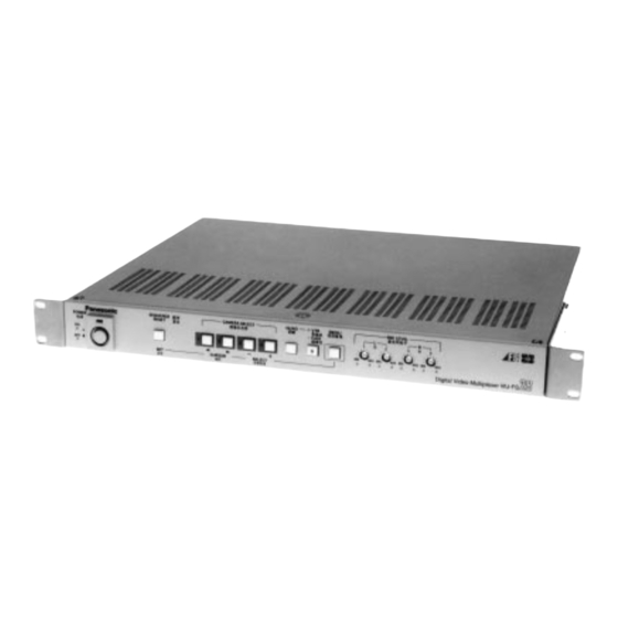
MAJOR OPERATING CONTROLS AND THEIR FUNCTIONS 1. Power On/Off Button (POWER ON/OFF) In the Camera Mode Used to turn on/off the power of this unit. The desired camera picture is selected on the monitor This indicator lights when turning on the power. by pressing one of these buttons. - Page 5 4. Quad Button (QUAD) 12. Recording Output Jack (REC OUT) (Pin-jack) This button should be used in the VTR playback mode. The recording signal for the VTR is provided via this The single playback picture turns to quad playback pic- connector.
- Page 6 INSTALLATIONS Picture Stability Switch ON/OFF Switching the microphone sensitivity For reasons of the specifications of this set, reproduced When using the microphone, set the Microphone pictures will swing vertically if three cameras are con- Sensitivity Switch inside this unit to the suitable position nected (with one channel left unconnected) for record- as shown below according to the sensitivity of the micro- ing.
- Page 7 Note on Installation : Mounting into the Rack Be sure to have your dealer install the set. Make sure that the power switch is OFF and that the power plug When this unit is to be mounted on a EIA 19-inch rack, has been pulled out of the electrical outlet in advance.
- Page 8 CONNECTIONS A. Basic System Refer to the connection diagram shown below for the basic system. Microphone 4 Microphone 1 Camera 4 Camera 1 VIDEO IN AUDIO IN VIDEO POWER PUSH NTSC (3.58) M.NTSC (4.43) 1450 INPUT SELECT Video Monitor GP-CM VIDEO VIDEO AUDIO...
- Page 9 B. Application Mini CCTV Camera 1 Video Monitor Mini CCTV WV-CM1450 etc. Camera 4 Microphone 4 Microphone 1 VIDEO IN AUDIO IN VIDEO POWER PUSH NTSC (3.58) M.NTSC (4.43) 1450 INPUT SELECT Video Monitor GP-CM Camera Drive Unit WV-PS104B VIDEO VIDEO AUDIO AUDIO...
-
Page 16: Circuit Description Ic Description
CIRCUIT DESCRIPTION IC Description 1. Main Board 1.1. IC806, IC811, IC820 and IC850 on the Main Board are using the 8-Bit A/D Converter IC YWCXD1175AM. Description of this IC is as follows: 24 DV Pin Name Description 23 VRB DVss 1 OE Output Enable signal input terminal. - Page 17 1.2. IC801 and IC802 on the Main Board are using the Write Control Gate Array Logic IC YWL7A1329. Description of this IC is as follows: 80 V DR13 122 79 PB0 DR12 123 78 PB1 77 PB2 DR11 124 DR10 125 76 PB3 75 PB4 DR9 126...
- Page 18 Name Description Name Description 33 CHANGE I CHANGE signal input terminal. 80 V – Power supply terminal. 34 LOCRST I LOCRST signal input terminal. 81 V – Power supply terminal. 35 SCASC I SCASC 82 PHCODR O PHCODR signal output terminal. 36 UL I UL signal input terminal.
- Page 19 1.3. IC908 on the Main Board is using the Real Time Name Description Clock with Crystal IC YWMSM62X42BR. 127 DR8 O RBDR Data input terminal. (18-Bit) Description of this IC is as follows: 128 Vss – Ground terminal. 129 DR8 STD.
- Page 20 1.4. IC803 on the Main Board is using the Memory Control Gate Array Logic IC YWM60065702. Description of this IC is as follows: Vss2 121 80 Vss2 Vss1 122 79 Vss1 BST2 123 78 MEMSEL 77 PASS BST3 124 76 RFLD BST4 125 BST5 126 75 R2FV2...
- Page 21 Name Description Name Description 25 HPHS0 I HPHS0 signal input terminal. 75 R2FV2 O R2FV2 signal output terminal. 76 RFLD O RFLD signal output terminal. 26 YHS2 I YHS2 signal input terminal. 77 PASS I PASS signal input terminal. 27 YHS1 I YHS1 signal input terminal.
- Page 22 1.5. IC909 on the Main Board is using the Voltage Name Description Detector IC YWM51957BFP. 123 BST2 I BST2 signal input terminal. Description of this IC is as follows: 124 BST3 I BST3 signal input terminal. 125 BST4 I BST4 signal input terminal. 126 BST5 I BST5 signal input terminal.
- Page 23 1.7. IC102, IC202 and IC302 on the Main Board are using the Chroma Difference Decoder IC YWM51271FP. Description of this IC is as follows: BF G 28 SYNC OUT Name Description BF GW 27 SEP LEV 1 BF G O Burst Gate Pulse position output terminal.
- Page 24 1.8. IC832 to IC843 on the Main Board are using the Field Memory IC YWM5M4C500AV. Description of this IC is as follows: Vss 22 21 Vcc A8/A0 SID1 23 20 SOE Input Row Address SID2 24 19 SIE IR1/A1 Counter SID3 25 18 SOC SOD1 26...
- Page 25 1.9. IC918 on the Main Board is using the Sync Signal Generator IC MN676021PPS. Description of this IC is as follows: Vcc1 28 Vcc2 Name Description 27 Vss2 1 Vcc1 – +5V supply terminal for Chroma Vss1 Subcarrier. 26 SYNC EX4fscI 2 Vss1 –...
- Page 26 1.10. IC914 and IC915 on the Main Board are using the Character Generator IC MB90077PF104. Description of this IC is as follows: N.C. 20 N.C. SCLK 19 HSYNC SCLK 18 VSYNC 17 VBB Register VMOD 16 VBG Control Bus (TOP VIEW) 15 VBR Data 14 VOB...
- Page 27 1.11. 1.13. IC51, IC54, IC101, IC201 and IC301 on the Main IC408 to IC410 on the Main Board are using the 12- Board are using the Analog Multiplexer/Demultiplexer Stage Binary Ripple Counter IC MC74HC4040AF. IC UPD74HC4051G. Description of this IC is as follows: Description of this IC is as follows: Q12 1 16 Vcc...
- Page 28 1.15. 1.17. IC52 on the Main Board is using the 3-Input Video IC104 on the Main Board is using the Sync Separator Switch with Clamp Circuit IC YWNJM2244M. IC YWNJM2229M. Description of this IC is as follows: Description of this IC is as follows: X’tal 1 1 16 AFC OUT 8 GND...
- Page 29 1.19. IC907 on the Main Board is using the 8K-word x 8-Bit CMOS S-RAM IC YWLH5168N80L. Description of this IC is as follows: Pin Name I/O Description N.C. 28 Vcc N.C. – Non connection 27 WE 26 CE2 25 A8 24 A9 23 A11 Address signal input terminals.
- Page 30 1.20. IC910 on the Main Board is using the 8-Bit Single Chip Microprocessor IC YW38004E8118. Description of this IC is as follows: RD 49 32 P20 WT 50 31 P21 P35 51 30 P22 P34 52 29 P23 28 P24 P32 53 27 P25 P32 54...
- Page 31 1.22. IC844 and IC903 on the Main Board are using the Name Description Hex D-FFs IC MC74HC174AF. 49 RD O Read signal output terminal. Description of this IC is as follows: 50 WT O Write signal output terminal. CLEAR 1 16 Vcc 51 P35 I/O P35 signal input/output terminal.
- Page 32 1.24. 1.26. IC911 on the Main Board is using the Octal 3-State IC846 on the Main Board is using the Quad 2-Input Bus Transceiver IC MC74HC245AF. NOR GAtes IC YWMC74HC02AF. Description of this IC is as follows: Description of this IC is as follows: 20 Vcc 1Y 1 14 Vcc...
- Page 33 1.28. 1.30. IC823, IC826, IC829 and IC830 on the Main Board IC106, IC204, IC304 and IC921 on the Main Board are using the Dual 4 to 1 Data Selectors IC are using the Hex Inverters IC YWMC74HC04AF. YWMC74HC153F. Description of this IC is as follows: Description of this IC is as follows: STROBE 1G 1 16 Vcc...
- Page 34 1.32. 1.34. IC407 on the Main Board is using the Triple 3-Input IC503 to IC506 on the Main Board are using the Dual AND Gates IC YWMC74HC11F. Operational Amplifiers IC YWUPC4570G. Description of this IC is as follows: Description of this IC is as follows: 1A 1 14 Vcc A OUT 1...
- Page 35 1.38. 2. Power Board IC53, IC105, IC845 and IC849 on the Main Board are using the 2-ch Multiplexer/Demultiplexer IC 2.1. IC1 on the Power Board are using the Switching YWTC4W53FUL. Regulator Controller IC YWFA5304P. Description of this IC is as follows: Description of this IC is as follows: Truth Table Out 1...
-
Page 36: Adjustment Procedure
Video Monitor with 75Ω. Upper Cover and remove the Upper Cover. Connect the Signal Generator to the Camera Input Connectors 1, 2 and 3 on the Rear Panel of the WJ-FS28. Remove six screws. Connect the prove of the Digital Voltmeter, Oscilloscope or Frequency Counter at the desired Test Point in each adjustment step. - Page 37 Supply the Ramp signal to the Camera Input Connectors Adjust CT201 to obtain 4.433618 MHz ± 5 Hz. 1, 2 and 3 on the Rear Panel of the WJ-FS28. Change the connection of the Frequency Counter to Press the CH1 button on the Front Panel.
- Page 38 Connect the terminated Oscilloscope with 75Ω to the Observing the Underscanned Video Monitor, fine adjust Recording Output Connector. the Horizontal difference of the Vertical Line of the Adjust VR402 so that the Luminance Pedestal level Crosshatch signal becomes minimum. becomes 0 mV as shown in Fig.
- Page 39 dø 100% 10° B – Y 0° 10° – 0 Fig. 4-10 Fig. 4-8 Supply the Colour Bar signal to the Camera Input 1 Adjust VR406 so that the Luminance level becomes 700 ± Connector on the Rear Panel. 14 mV as shown in Fig. 4-9. Connect the terminated Oscilloscope with 75Ω...
- Page 40 (7). RB Decoder Adjustment Phase Chroma Test Point: Recording Output Jack Rear Panel 103 ± 5° 220 ± 7° Adjust: VR201 (RB C-GAIN) Main Board 283 ± 7° 220 ± 7° VR202 (RB C-PHASE) Main Board 167 ± 8° 155 ± 10° Supply the Colour Bar signal to the Camera Input 2 Table 4-3 Connector on the Rear Panel.
- Page 41 Adjust CT902 so that the difference between the Character Divider Line Position t and t becomes within ± 1 µs as shown in Fig. 4-18. Fig. 4-15 Connect the terminated Oscilloscope with 75Ω to the Character Character Recording Output Jack. Adjust CT901 so that the difference between the 20% Setup Character Position t...
-
Page 42: Chip Components
CHIP COMPONENTS 2. Chip Diode 1. Chip Transistor The diode number is indicated on the top surface of the chip The transistor number is indicated on the top surface of the diode using two alphabet letters. chip transistor using two alphabet letters or one numerical number and two alphabet letters. -
Page 48: Schematic Diagram Main Board (1/3)
Printed in Japan C-609 N 5, 7, 23...