Table of Contents
Advertisement
Advertisement
Table of Contents

Related Manuals for GE V7768


Summary of Contents for GE V7768
- Page 1 Intelligent Platforms Hardware Reference V7768/V7769* ® Intel Core™ Duo Processor VME Single Board Computer THE V7768/V7769 IS DESIGNED TO MEET THE EUROPEAN UNION (EU) RESTRICTIONS OF HAZARDOUS SUBSTANCE (ROHS) DIRECTIVE (2002/95/EC) CURRENT REVISION. Publication No: 500-9300007768-000 Rev. E...
- Page 2 January 4, 2012 Waste Electrical and Electronic Equipment (WEEE) Returns GE is registered with an approved Producer Compliance Scheme (PCS) and, subject to suitable contractual arrangements being in place, will ensure WEEE is processed in accordance with the requirements of the WEEE Directive.
-
Page 3: Table Of Contents
1.2.1 V7768 Board Layout Information ........ - Page 4 A.2.1 V7768 PCI-X PMC Site Connector and Pinout (J11) ....... .
-
Page 5: List Of Figures
Figure 1-4 Installing the PMC Card on the V7768/V7769 ....... . -
Page 6: List Of Tables
Table A-3 V7768 PCI-X PMC Site Connector Pinout (J11) ....... . - Page 7 Table A-13 Mezzanine PCI-X PMC Site Connector Pinout (J23) ..........72 Table A-14 Mezzanine PCI-X PMC Site Connector Pinout (J24) .
-
Page 8: Overview
PCI-to-VME bridge, allowing your board to function as a system controller or peripheral CPU in multi-CPU systems. The V7768 is a single-slot board, and the V7769 is a dual-slot board. The V7769 has the same functionality as the V7768 and also connects to the ACC-0623* (which will be referred to as the mezzanine board throughout this manual), making it a dual-slot board. - Page 9 • Real-Time clock/calendar • Front panel reset switch • PS/2 Keyboard/Mouse connection (front I/O) • Onboard parallel connector The 945GM chipset allows the V7768/V7769 to be capable of executing many of ® ® today’s desktop operating systems such as Microsoft ’s Windows...
- Page 10 • Remote booting out the front panel only • Up to 8 GByte of bootable CompactFlash (optional) • PCI-X capable PMC site with VITA 35 P2 I/O (factory populated on V7768 and main board of V7769) • VITA 1-1994 with byte swap •...
- Page 11 Intel 945GM Chipset The V7768/V7769 incorporate the latest Intel chipset technology, the 945GM. The Intel 945GM chipset is an optimized integrated graphics solution with up to a 667 MHz system bus. The chipset has a low power design, advanced power management, supporting up to 2 GByte of DDR2 system memory.
-
Page 12: Figure 1 V7768 Block Diagram
Figure 1 V7768 Block Diagram Intel Core 2 Duo Celeron M Processor 667MHz DDR2 Memory Up to 2 GByte SODIMM FPGA NVRAM DDR2 Intel PCIe x8 945GM Express PEX8114 Up to 8 GByte PCIe-PCIX LEDs CompactFlash Bridge Reset PCIX 133MHz... -
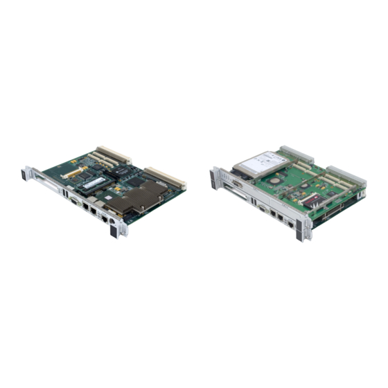
Page 13: Figure 2 Illustration Of V7768
Figure 2 Illustration of V7768 Overview 13... -
Page 14: Figure 3 V7769 Block Diagram
Figure 3 V7769 Block Diagram SATA 2 x SAS PCI-X LSI1064 SAS/SATA Site 1 Controller PEX8518 PCIE Switch SATA to IDE Converter PCI-X Site 2 Up to 4 GByte PEX8114 CompactFlash PCIE-PCIX Bridge Vita 35 14 V7768/V7769 Hardware Reference Manual... -
Page 15: Figure 4 Illustration Of V7769
Figure 4 Illustration of V7769 Overview 15... - Page 16 Appendix B - AMI BIOS Setup Utility describes the menus and options associated with the American Megatrends, Inc (system) BIOS. Appendix C - Remote Booting describes the menus and selections necessary to boot from the SBC remotely. 16 V7768/V7769 Hardware Reference Manual...
- Page 17 References Intel Celeron M Processor on 65 nm Processor January 2007, Order Number 312726-004 ® Intel Core 2 Duo Processor for Intel Centrino Duo Processor Technology Process Datasheet September 2007, Revision 004, Order Number 314078-004 Mobile Intel 945 Express Chipset Family November 2006, Order Number 309219-003 Intel I/O Controller Hub 7 (ICH 7) Family Datasheet January 2006, Order Number 307013-002...
- Page 18 Parts or Modify parts or perform any unauthorized modification to the product. Return the System product to GE for service and repair to ensure that safety features are maintained. Dangerous Warnings, such as the example below, precede only potentially dangerous Procedure procedures throughout this manual.
- Page 19 Warnings, STOP Cautions Informs the operator that a practice or procedure should not be performed. Actions could result in and Notes injury or death to personnel, or could result in damage to or destruction of part or all of the system.
-
Page 20: Installation And Setup
All claims arising from shipping damage should be filed with the carrier and a complete report sent to GE Customer Care along with a request for advice concerning the disposition of the damaged item(s). -
Page 21: V7768 Board Layout Information
1.2.1 V7768 Board Layout Information Figure 1-1 V7768 Connector Locations CompactFlash (used for V7769 version) SODIMM SVGA 1 3 5 1 3 INDICATES PIN 1 COM1 Installation and Setup 21... -
Page 22: Table 1-1 V7768 Connectors And Switches
Table 1-1 V7768 Connectors and Switches Connector Function VME interface connector USB 2.0, Serial ATA, digital video, COM3 and COM4, Gigabit Ethernet CompactFlash socket SODIMM socket J29 and J30 USB ports Mouse/Keyboard PS/2 Type connector J15 and J18 Gigabit Ethernet connectors... -
Page 23: Table 1-4 Vme System Controller - Switch (S10)
Table 1-4 VME System Controller - Switch (S10) Position State Function Force VME controller based on 2-3 state Enable auto system controller Force system controller (any slot) Force non-system controller (any slot) Table 1-5 Battery Enable - Switch (S11) Position State Function Enable Battery... -
Page 24: Figure 1-2 Com1 Termination Headers (E13, E14, E17)
RS422 w/o Termination 1-3, 2-4 Both Out Figure 1-2 COM1 Termination Headers (E13, E14, E17) 1 3 5 1 3 1 3 5 1 3 1 3 5 1 3 RS232 RS422 w/Termination RS422 w/o Termination 24 V7768/V7769 Hardware Reference Manual... -
Page 25: Mezzanine Board Layout Information (V7769)
1.2.2 Mezzanine Board Layout Information (V7769) Figure 1-3 Mezzanine Board Connector Locations Installation and Setup 25... -
Page 26: Table 1-8 Mezzanine Connectors And Switches
2.5 in. SATA drive connector SAS connector Header Function SMBus debug header Not Used Not Used Switches Function Reserved Enable/Disable JTAG Table 1-9 Switch (S2) Settings Position State Function Disable JTAG Enable JTAG Not Used Not Used 26 V7768/V7769 Hardware Reference Manual... -
Page 27: Installation
The following steps describe the GE-recommended method for installation and powerup of the V7768/V7769: 1. If a PMC module is to be used, connect it to the V7768/V7769 prior to board installation (as shown in Figure 1-4 on page 28). Refer to the Product Man- ual for the PMC module for configuration and setup. -
Page 28: Figure 1-4 Installing The Pmc Card On The V7768/V7769
Figure 1-4 Installing the PMC Card on the V7768/V7769 28 V7768/V7769 Hardware Reference Manual... -
Page 29: Figure 1-5 Backside Mounting For The Pmc Card
Figure 1-5 Backside Mounting for the PMC Card Installation and Setup 29... -
Page 30: Figure 1-6 Installation Of Mezzanine Board Onto The Main Board
Figure 1-6 Installation of Mezzanine Board onto the Main Board See Figure 4 on page 15 for the image of the fully installed V7769. 30 V7768/V7769 Hardware Reference Manual... -
Page 31: Front/Rear Panel Connectors
Gigabit Ethernet port, one 10/100 RJ45 connector, one serial port, SVGA, keyboard/mouse, the manual reset switch and the status LEDs. A drawing of the V7768/V7769 front panels are shown in Figure 1-7 and Figure 1-8. The front panel connectors and indicators are labeled as follows: V7768 •... -
Page 32: Front Panel Layouts
1.5 Front Panel Layouts Figure 1-7 V7768 Front Panel Layout Status LEDs (from left to right) Boot Done (B) Booting - Indicates BIOS Boot is in progress. When LED is Off, CPU has finished POST and is ready (Red LED). -
Page 33: Figure 1-8 Mezzanine Front Panel Layout (For V7769)
Figure 1-8 Mezzanine Front Panel Layout (for V7769) Status LEDs (from top to bottom) SATA SerialATA Activity - LED will flash to indicate activity on the SATA drive, (Green LED). SAS1 SCSI Activity - LED will flash to indicate activity on the first SAS Lane, (Green LED). -
Page 34: Standard Features
The following sections describe the standard features of the V7768/V7769. 2.1 BGA CPU The V7768 is factory populated with either an Intel Core 2 Duo or Celeron M processor. The V7769 is factory populated with an Intel Core 2 Duo processor. -
Page 35: Memory Map
The V7768/V7769 include 32 KByte of non-volatile SRAM which can be accessed by the CPU at any time, and is used to store system data that must not be lost during power-off conditions. NOTE Memory capacity may be extended as parts become available. -
Page 36: Table 2-2 V7768/V7769 I/O Address Map
2048 Reserved *While these I/O ports are reserved for the listed functions, they are not implemented on the V7768/ V7769. They are listed here to make the user aware of the standard PC usage of these ports. 36 V7768/V7769 Hardware Reference Manual... -
Page 37: Interrupts
The interrupt number in HEX and decimal are also defined for real and protected mode in Table 2-4 on page 38. The interrupt hardware implementation on the V7768/V7769 is standard for computers built around the PC architecture, which evolved from the IBM PC/XT. -
Page 38: Table 2-4 Interrupt Vector Table
Same as Real Mode DOS Absolute Disk Read Same as Real Mode DOS Absolute Disk Write Same as Real Mode DOS Program Terminate, Same as Real Mode Stay Resident DOS Keyboard Idle Loop Same as Real Mode 38 V7768/V7769 Hardware Reference Manual... - Page 39 Table 2-4 Interrupt Vector Table (Continued) Interrupt No. IRQ Line Real Mode Protected Mode DOS CON Dev. Raw Output Same as Real Mode DOS 3.x+ Network Comm Same as Real Mode DOS Internal Use Same as Real Mode DOS Internal Use Same as Real Mode DOS Internal Use Same as Real Mode...
-
Page 40: Pci Interrupts
For a single function device, only INTA# may be used while the other three interrupt lines have no meaning. Figure 2-1 on page 42 depicts the V7768/V7769 interrupt logic pertaining to FPGA timer operations and the PCI expansion site. -
Page 41: Table 2-5 Pci Device Interrupt Mapping By The Bios
Vendor ID Device ID ID Select PCI IRQ Request Line PCI-to-VME Bridge Tundra Universe IID 0x10E3 0x0000 AD27 INTD REQ1 Timer/SRAM FPGA GE Proprietary 0x114A 0x0004 AD26 INTC AD24 INTA, B, C, D REQ0 Ethernet Controller Intel 82571EB 0x8086 0x105E... -
Page 42: Integrated Peripherals
PMC237 FPGA 2.6 Integrated Peripherals The V7768/V7769 incorporate an SMSC Super I/O (SIO) chip. The SIO provides the V7768/V7769 with two 16550 UART-compatible serial ports, keyboard and mouse ports, and general purpose I/O for system functions, available via the VME backplane connectors. -
Page 43: Ethernet Controller
The RJ45 connector is used with the 10Base-T standard. 10Base-T has a maximum length of 100 meters. 100Base-TX The V7768/V7769 also support the 100Base-TX Ethernet. A network based on a 100Base-TX standard uses unshielded twisted-pair cables. 100Base-TX has a maximum length of 100 meters. -
Page 44: Video Graphics Adapter
2.8 Video Graphics Adapter The SVGA port on the V7768/V7769 is controlled by the Intel 945GM Graphic and Memory Controller Hub (GMCH). The GMCH is hardware and BIOS compatible with the industry SVGA and digital video standards supporting both VESA high- resolution and extended video modes. -
Page 45: Embedded Pc/Rtos Features
The V7768/V7769 support High Throughput DMA transfers of bytes, words and longwords in both Master and Slave configurations. If Endian conversion is not needed, GE offers a special “Bypass” mode that can be used to further enhance throughput (not available for byte transfers). -
Page 46: I2C/Smbus Temperature Sensor
C/SMBus Temperature Sensor The MAX6659MEE can be monitored and controlled on the SMBus at address 0x98 for the V7768/V7769. This will allow the user to monitor and set up the alarm (OVERT2). For more information on the Maxim MAX6659MEE contact them directly at: 1-888-629-4642, or visit Maxim’s website at www.maxim-ic.com. -
Page 47: Timers
3.3 Timers The V7768/V7769 provide four user-programmable timers (two 16-bit and two 32-bit) which are completely dedicated to user applications and are not required for any standard system function. Each timer is clocked by independent generators with selectable rates of 2 MHz, 1 MHz, 500 kHz and 250 kHz. Each timer may be independently enabled and each is capable of generating a system interrupt on timeout. -
Page 48: Timer Control Status Register 2 (Tcsr2)
Timers 1 & 2 are 16-bits wide and obtain their load count from the Timer 1 & 2 Load Count Register (TMRLCR12), located at offset 0x10 from the address in BAR2. The mapping of bits in this register is shown in Table 3-5. 48 V7768/V7769 Hardware Reference Manual... -
Page 49: Timer 3 Load Count Register (Tmrlcr3)
Table 3-5 TMRLCR12 Bit Mapping Field Bits Read or Write Timer 2 Load Count TMRLCR12[31..16] Timer 1 Load Count TMRLCR12[15..0] When either of these fields are written (either by a single 32-bit write or separate 16-bit writes), the respective timer is loaded with the written value on the next rising edge of the timer clock, regardless of whether the timer is enabled or disabled. -
Page 50: Timer 3 Current Count Register (Tmrccr3)
The Timer 2 IRQ Clear (T2IC) register is used to clear an interrupt caused by Timer 2. Writing to this register, located at offset 0x34 from the address in BAR2, causes the interrupt from Timer 2 to be cleared. This can also be done by writing a 50 V7768/V7769 Hardware Reference Manual... -
Page 51: Timer 3 Irq Clear (T3Ic)
Register (TCSR1). This register is write only and the data written is irrelevant. 3.4 Watchdog Timer The V7768/V7769 provide a programmable Watchdog Timer (WDT) which can be used to reset the system if software integrity fails. 3.4.1 WDT Control Status Register (WCSR) The WDT is controlled and monitored by the WDT Control Status Register (WCSR) which is located at offset 0x08 from the address in BAR2. -
Page 52: Wdt Keepalive Register (Wkpa)
3.5 NVRAM The V7768/V7769 provide 32 KByte of non-volatile RAM. This memory is mapped in 32K of address space starting at the address in BAR1. This memory is available at any time and supports byte, short word and long word accesses from the PCI bus. -
Page 53: Vme Control
8 GByte. This CompactFlash Disk appears to the user as an intelligent ATA (IDE) disk drive with the same functionality and capabilities as a “rotating media” IDE hard drive. The V7768 BIOS includes an option to allow the board to boot from the CompactFlash with user-provided operating system. -
Page 54: Remote Ethernet Booting
3.8 Remote Ethernet Booting The V7768/V7769 is capable of booting from a server using Gigabit Ethernet over a network utilizing the Boot ROM BIOS. The BIOS gives you the ability to remotely boot the V7768/V7769 using a PXE network protocol. The Ethernet must be connected through the GbE front panel (RJ45) connector to boot remotely. -
Page 55: Maintenance
8. Quality of cables and I/O connections If products must be returned, contact GE for a Return Material Authorization (RMA) Number. This RMA Number must be obtained prior to any return from Customer Care. - Page 56 Compliance This chapter provides the applicable information regarding regulatory compliance for the V7768/V7769. GE’s V7768/V7769 have been evaluated and has met the requirements for compliance to the following standards: International Compliance • EN55022:1998/CISPR 22:1997 • IEC61000-4-2 • IEC61000-4-3 • IEC61000-4-4 •...
- Page 57 Changes or modifications not expressly approved by the party responsible for compliance could void the user's authority to operate the equipment. Canadian Regulations The V7768/V7769 Class A digital apparatus comply with Canadian ICES-003. NOTE Any equipment tested and found compliant with FCC Part 15 for unintentional radiators or EN55022 (previously CISPR 22) satisfies ICES-003.
-
Page 58: A • Appendix A: Connector Pinouts
A • Appendix A: Connector Pinouts The V7768/V7769 have several connectors for their I/O ports. Wherever possible, the V7768/V7769 use connectors and pinouts typical for any desktop PC. This ensures maximum compatibility with a variety of systems. Figure A-1 shows the layout of the connectors on the V7768. -
Page 59: Figure A-2 V7769 Connector Pinout
Figure A-2 V7769 Connector Pinout Appendix A: Connector Pinouts 59... -
Page 60: V7768 Vme Connectors And Pinouts (P1 And P2)
A.1 V7768 VME Connectors and Pinouts (P1 and P2) Figure A-3 shows the orientation of the P1 and P2 connectors on the V7768. Table A-1 shows the pinout for the VME P1 and P2 connectors. Figure A-3 VME Connectors (P1/P2) -
Page 61: Table A-2 V7768 Vme Connector Pinout (P2)
Table A-2 V7768 VME Connector Pinout (P2) Pin No. Row A Row B Row C Row D Row Z SP1_TX CONN[1] CONN[2] USB_P5N SP1_RTS# CONN[3] USB_P5P SP1_DTR# CONN[4] CONN[5] USB_OC5# SP1_RX CONN[6] SP1_DCD# CONN[7] CONN[8] USB_P4N SP1_CTS# CONN[9] USB_P4P SP1_DSR#... -
Page 62: V7768 Pci-X Pmc Connectors
A.2 V7768 PCI-X PMC Connectors A.2.1 V7768 PCI-X PMC Site Connector and Pinout (J11) The PCI Mezzanine Card (PMC) carries the same signals as the PCI standard; however, the PMC standard uses a completely different form factor. Tables A-3 through A-5 show the pinouts for the PMC site connectors. -
Page 63: V7768 Pci-X Pmc Site Connector And Pinout (J12)
A.2.2 V7768 PCI-X PMC Site Connector and Pinout (J12) Figure A-5 V7768 PCI-X PMC Site Connector (J12) Table A-4 V7768 PCI-X PMC Site Connector Pinout (J12) PMC Connector (J12) PMC Connector (J12) Left Side Right Side Left Side Right Side... -
Page 64: V7768 Pci-X Pmc Site Connector And Pinout (J13)
A.2.3 V7768 PCI-X PMC Site Connector and Pinout (J13) Figure A-6 V7768 PCI-X PMC Site Connector (J13) Table A-5 V7768 PCI-X PMC Site Connector Pinout (J13) PMC Connector (J13) PMC Connector (J13) Left Side Right Side Left Side Right Side... -
Page 65: Mezzanine Pci-X Pmc Site Connector And Pinout (J14)
A.2.4 Mezzanine PCI-X PMC Site Connector and Pinout (J14) Figure A-7 Mezzanine PCI-X PMC Site Connector (J14 ) Table A-6 Mezzanine PCI-X PMC Site Connector Pinout (J14 ) PMC Connector (J14) PMC Connector (J14) Left Side Right Side Left Side Right Side Name Name... -
Page 66: V7769 Mezzanine Backplane Connectors (P1 And P2)
Signal Signal Signal Signal Signal +5 V BG0IN# BG0OUT# BG1IN# BG1OUT# BG2IN# BG2OUT# BG3IN# BG3OUT# +5 V IACKIN# IACKOUT# -12 V +12 V +5 V +5 V +5 V +5 V N/C indicates No Connection 66 V7768/V7769 Hardware Reference Manual... -
Page 67: V7769 Mezzanine Pci-X Pmc Site 1 Connectors
A.4 V7769 Mezzanine PCI-X PMC Site 1 Connectors A.4.1 Mezzanine PCI-X PMC Site 1 Connector and Pinout (J11) The PMC carries the same signals as the PCI standard; however, the PMC standard uses a completely different form factor. Tables A-8 through A-10 show the pinouts for the PMC site connectors. -
Page 68: Mezzanine Pci-X Pmc Site 1 Connector And Pinout (J12)
VCC_3.3 SERR# BMODE2# VCC_3.3 CBE[1]# PCIB_RESET# BMODE3# AD[14] AD[13] VCC_3.3 BMODE4# M66EN AD[10] AD[8] VCC_3.3 AD[30] AD[29] AD[7] AD[26] VCC_3.3 AD[24] VCC_3.3 PMC_IDSEL AD[23] VCC_3.3 AD[20] AD[18] ACK64# VCC_3.3 AD16] CBE[2]# N/C indicates No Connection 68 V7768/V7769 Hardware Reference Manual... -
Page 69: Mezzanine Pci-X Pmc Site 1 Connector And Pinout (J13)
A.4.3 Mezzanine PCI-X PMC Site 1 Connector and Pinout (J13) Figure A-11 Mezzanine PCI-X PMC Site Connector (J13 ) Table A-10 Mezzanine PCI-X PMC Site Connector Pinout (J13 ) PMC Connector (J13) PMC Connector (J13) Left Side Right Side Left Side Right Side Name Name... -
Page 70: V7769 Mezzanine Pci-X Pmc Site 2 Connectors
AD[15] GNT0# AD[12] AD[11] REQ0# VCC_5.0 AD[9] VCC_5.0 VCC_3.3 AD[31] CBE[0]# AD[28] AD[27] AD[6] AD[5] AD[25] AD[4] CBE[3]# VCC_3.3 AD[3] AD[22] AD[21] AD[2] AD[1] AD[19] VCC_5.0 AD[0] VCC_5.0 VCC_3.3 AD[17] REQ64# N/C indicates No Connection 70 V7768/V7769 Hardware Reference Manual... -
Page 71: Mezzanine Pci-X Pmc Site 2 Connector And Pinout (J22)
A.5.2 Mezzanine PCI-X PMC Site 2 Connector and Pinout (J22) Figure A-13 Mezzanine PCI-X PMC Site Connector (J22) Table A-12 Mezzanine PCI-X PMC Site Connector Pinout (J22) PMC Connector (J22) PMC Connector (J22) Left Side Right Side Left Side Right Side Name Name Name... -
Page 72: Mezzanine Pci-X Pmc Site 2 Connector And Pinout (J23)
VCC_3.3 PAR64 AD[43] AD[42] AD[63] AD[62] AD[41] AD[61] AD[40] AD[60] AD[39] AD[38] AD[59] AD[58] AD[37] AD[57] AD[36] VCC_3.3 AD[56] AD[35] AD[34] AD[55] AD[54] AD[33] AD[53] VCC_3.3 AD[32] AD[52] AD[51] AD[50] AD[49] N/C indicates No Connection 72 V7768/V7769 Hardware Reference Manual... -
Page 73: Mezzanine Pci-X Pmc Site 2 Connector And Pinout (J24)
A.5.4 Mezzanine PCI-X PMC Site 2 Connector and Pinout (J24) Figure A-15 Mezzanine PCI-X PMC Site Connector (J24) Table A-14 Mezzanine PCI-X PMC Site Connector Pinout (J24) PMC Connector (J24) PMC Connector (J24) Left Side Right Side Left Side Right Side Name Name Name... -
Page 74: Usb Connectors And Pinout (J29 And J30)
(same for each). Figure A-16 USB Connector (J29 and J30) Table A-15 USB Connector Pinout (J29 and J30) Signal Function USB_VCC USB Power USB- USB Data - USB+ USB Data + USBG USB Ground 74 V7768/V7769 Hardware Reference Manual... -
Page 75: Gigabit Ethernet Connectors And Pinouts (J15 And J18)
A.7 Gigabit Ethernet Connectors and Pinouts (J15 and J18) The pinout diagram for the Gigabit Ethernet connector and pinout are shown in Figure A-17 and Table A-16. Figure A-17 Gigabit Ethernet Connector (J18) Connector Opening Pin #1 Top View Table A-16 Gigabit Ethernet Connector Pinout (J18) Signal Function Transmit Data... -
Page 76: Video Graphics Adapter And Pinout (J28)
The video port uses a standard high-density DB15 SVGA connector. Figure A-18 illustrates the pinout and Table A-17 gives a description. Figure A-18 SVGA Connector (J28) SVGA Table A-17 SVGA Connector Pinout (J28) Signal VGA_Video1_Red VGA_Video1_Green VGA_Video1_Blue VCC_5.0 VGA_DDC_Data VGA_HSYNC VGA_VSYNC VGA_DDC_CLK N/C indicates No Connection 76 V7768/V7769 Hardware Reference Manual... -
Page 77: Serial Connector And Pinout (J35)
A.9 Serial Connector and Pinout (J35) COM 1 serial port connector is a standard RJ45 connector as shown in Figure A-19 and its pinout in Table A-18. Figure A-19 Serial Connector (J35) Table A-18 Serial Connector Pinout (J35) RS232 Signal RS422 Signal RXD- RTS+... -
Page 78: Mouse/Keyboard Connector And Pinout (J38)
Table A-19 Mouse/Keyboard Connector Pinout (J38) Direction Function In/Out Mouse Data In/Out Keyboard Data Ground +5 V Mouse Clock Keyboard Clock Shield Chassis Ground An adapter cable is included with the V7768/V7769 to separate the keyboard and mouse connectors. 78 V7768/V7769 Hardware Reference Manual... -
Page 79: Figure A-21 Mouse/Keyboard Splitter Cable
Figure A-21 Mouse/Keyboard Splitter Cable Table A-20 Mouse/Keyboard Splitter Cable Pinout Keyboard Mouse Direction Function Direction Function In/Out Keyboard Data In/Out Mouse Data Unused Unused Ground Ground +5 V +5 V Keyboard Clock Mouse Clock Unused Unused Shield Chassis Ground Shield Chassis Ground NOTE... -
Page 80: V7769 Mezzanine Sas Connector And Pinout (J28)
A.11 V7769 Mezzanine SAS Connector and Pinout (J28) Figure A-22 Mezzanine Connector (J28) Table A-21 Mezzanine SAS Connector Pinout (J28) Direction RX[0]+ RX[0]- RX[1]+ RX[1]- TX[1]- TX[1]+ TX[0]- TX[0]+ G1-G9 All pins not listed are not connected. 80 V7768/V7769 Hardware Reference Manual... -
Page 81: B • Appendix B: Ami Bios Setup Utility
B.1 First Boot Menu The V7768/V7769 have a First Boot pop up menu enabling the user to, on a one time basis, select a drive device to boot from. This feature is useful when installing from a bootable disk. -
Page 82: Main Menu
System Memory Size : 1016MB ←→ Select Screen ↑↓ Select Item System Time [11:39:40] Change Field System Date [Tue 03/04/2004] Select Field General Help Save and Exit Exit 002.53 (C) Copyright 1985-2002, American Megatrends, Inc. 82 V7768/V7769 Hardware Reference Manual... -
Page 83: Advanced Bios Setup Menu
B.3 Advanced BIOS Setup Menu The Advanced BIOS Setup menu allows the user to configure some CPU settings, the IDE bus, other external devices and internal drives. Select the Advanced tab from the ezPORT setup screen to enter the Advanced BIOS Setup screen. -
Page 84: Pci/Pnp Setup Menu
IRQ4 [Available] ←→ Select Screen IRQ5 [Available] ↑↓ Select Item IRQ7 [Available] Change Option IRQ9 [Available] General Help IRQ10 [Available] Save and Exit IRQ11 [Available] Exit IRQ14 [Available] 002.53 (C) Copyright 1985-2002, American Megatrends, Inc. 84 V7768/V7769 Hardware Reference Manual... -
Page 85: Boot Setup Menu
B.5 Boot Setup Menu Use the Boot Setup menu to set the priority of the boot devices, including booting from a remote network. The devices shown in this menu are the bootable devices detected during POST. If a drive is installed that does not appear, verify the hardware installation. -
Page 86: Security Setup Menu
002.53 (C) Copyright 1985-2002, American Megatrends, Inc. To reset the security in the case of a forgotten password you must clear the NVRAM and reconfigure. Refer to Chapter 1 “Installation and Setup” for how to clear the CMOS password. 86 V7768/V7769 Hardware Reference Manual... -
Page 87: Chipset Setup Menu
B.7 Chipset Setup Menu Select the various options for chipsets located in the system (for example, the CPU configuration and configurations for the North and South Bridge). The settings for the chipsets are processor dependent and care must be used when changing settings from the defaults set at the factory. -
Page 88: Exit Menu
002.53 (C) Copyright 1985-2002, American Megatrends, Inc. If changes have previously been made in the BIOS and the system malfunctions, reboot the system and access this screen. Select ‘Load Failsafe Defaults’ and continue the reboot. 88 V7768/V7769 Hardware Reference Manual... -
Page 89: C • Appendix C: Remote Booting
C • Appendix C: Remote Booting The V7768/V7769 include a Boot-from-LAN BIOS option which allows the SBCs to be booted from a network. This appendix describes the procedures to enable this option and to select a LAN connection as the boot device. -
Page 90: Boot Menus
First Boot menu. Selecting Network:IBA GE Slot to boot from the LAN in this screen applies to the current boot only. At the next reboot the V7768/V7769 will revert back to the setting in the Boot menu. -
Page 91: Boot Menu
Once you press CTRL-S, the Boot Agent setup menu will appear. PXE is the boot option available on the V7768/V7769. You can change the settings for the Setup Prompt and Setup Menu Wait Time. You can either enable or disable the prompt, and you can set the amount of wait time for the setup menu. - Page 92 © 2012 GE Intelligent Platforms Embedded Systems, Inc. All rights reserved. Information Centers For more information, please visit * indicates a trademark of GE Intelligent Platforms, Inc. and/or its affiliates. All other the GE Intelligent Platforms Embedded Americas: trademarks are the property of their respective...