Kenwood NX-5800 Service Manual
Uhf digital transceiver
Hide thumbs
Also See for NX-5800:
- Service manual (150 pages) ,
- Common function reference (476 pages) ,
- Function reference (190 pages)
Table of Contents
Advertisement
SERVICE MANUAL
B5B-7161-10
11
2014
RA017<Rev.002>
COPYRIGHT © 2014 JVC KENWOOD Corporation
1
Precaution. . . . . . . . . . . . . . . . . . . . . . . . . . . . . . . . . . . . . . . . . . . . . . . . . . . . . . . . . . . . . . . . . . . . . . . . . 1-4
2
Specific Service Instructions . . . . . . . . . . . . . . . . . . . . . . . . . . . . . . . . . . . . . . . . . . . . . . . . . . . . . . 1-4
3
Disassembly . . . . . . . . . . . . . . . . . . . . . . . . . . . . . . . . . . . . . . . . . . . . . . . . . . . . . . . . . . . . . . . . . . . . . . 1-29
4
ADJUSTMENT . . . . . . . . . . . . . . . . . . . . . . . . . . . . . . . . . . . . . . . . . . . . . . . . . . . . . . . . . . . . . . . . . . . . . . . 1-32
5
Troubleshooting . . . . . . . . . . . . . . . . . . . . . . . . . . . . . . . . . . . . . . . . . . . . . . . . . . . . . . . . . . . . . . . . . 1-65
REVISED
This service manual has been revised due to the addition of NX-5800 type K and NX-5800(B) type F, K.
This product complies with the RoHS directive for the European market.
B5B-7161-10
SERVICE MANUAL
UHF DIGITAL TRANSCEIVER
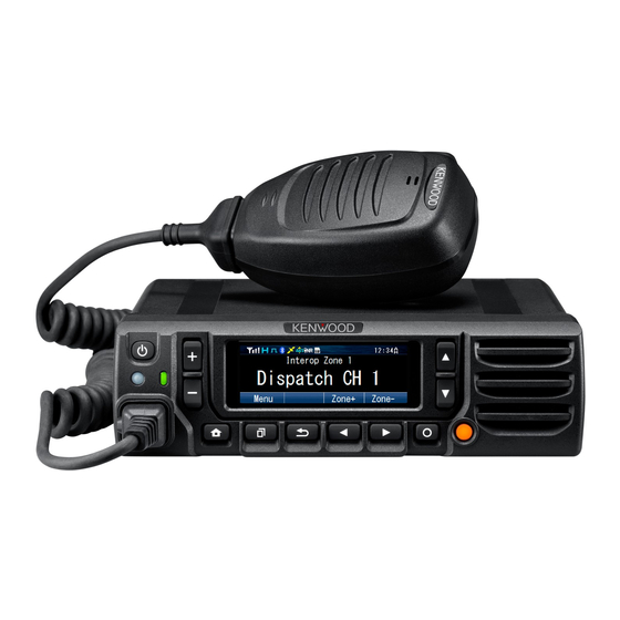
NX-5800, NX-5800(B)
NX-5800 is a model that operation panel is attached.
NX-5800(B) is a model that operation panel is not attached.
The illustration is NX-5800.
Note :
Lead free solder used in the board (material : Sn, Ag, In, Bi, melting point : 227 Centigrade)
COPYRIGHT © 2014 JVC KENWOOD Corporation
TABLE OF CONTENTS
This product uses Lead Free solder.
No.RA017<Rev.002>
2014/11
Advertisement
Table of Contents

Related Manuals for Kenwood NX-5800


Summary of Contents for Kenwood NX-5800
- Page 1 TROUBLESHOOTING ..............1-65 REVISED This service manual has been revised due to the addition of NX-5800 type K and NX-5800(B) type F, K. This product complies with the RoHS directive for the European market.
- Page 2 Neither is any liability assumed for damages resulting from the use of the information contained herein. JVC KENWOOD Corporation reserves the right to make changes to any products herein at any time for improvement purposes. Firmware Copyrights The title to and ownership of copyrights for firmware embedded in KENWOOD product memories are reserved for JVC KENWOOD Corporation.
- Page 3 Less than 2% Modulation 16K0F3E, 11K0F3E, 8K30F1E, 8K30F1D, 8K30F7W, 4K00F1E, 4K00F1D, 4K00F7W, 4K00F2D, 8K10F1W, 8K10F1E, 8K10F1D Measurements made per TIA/EIA-603 and specifications shown are typical. JVC KENWOOD Corporation reserves the right to change specifications without prior notice or obligation. (No.RA017<Rev.002>)1-3...
-
Page 4: Precaution
Choose the type of transceiver NX-5800(B) K 380~470 NX-5800 K2 NX-5800(B) F2 NX-5800(B) K2 NX-5800(B) As of October 2014, NX-5800 or NX-5800(B)? Operation panel KCH-19 is available. NX-5800 Are you using Refer to the “2.3.1 Ignition Sense KCT-46 the ignition sense cable? Cable (Option)”. - Page 5 ] + Power ON Select the “Panel Test” using the [ ] / [ ] key. Press the [ ] key. PC mode Received commands from PC Panel tuning mode [Panel test mode] + [ The illustration is NX-5800. KPG-46U Transceiver Fig.1 (No.RA017<Rev.002>)1-5...
- Page 6 2.2.6.3 Programming correct. If password is incorrect, “Input Password” is re- (1) Start up the firmware programming software (KENWOOD displayed. Firmware Loader). The KFL.exe exists in the KPG-D1/D1N - How to enter password using the [ ] and [ ] keys;...
- Page 7 4 Channel Channel Space Analog: 12.5kHz/25kHz programmed to the target. Spacing • “Model name” must be same to clone the transceiver. NXDN: 6.25kHz/12.5kHz The illustration is NX-5800. P25: 12.5kHz 5 RX Signaling RX QT/DQT Receive QT/DQT 6 TX Signaling TX QT/DQT...
- Page 8 • Key operation Key\Item Zone Select Channel RX Frequency TX Frequency Channel Channel RX Signaling TX Signaling Select Type Spacing Decision Decision Decision Decision Decision Decision Decision Decision Unused Back to the Back to the pre- Back Back to the Back to the Back to the Back to the...
- Page 9 • Direct enter mode Key\Item Channel Frequency Frequency Signaling Signaling Name Decision Character/Channel name decision Delete Unused Exit panel program mode Unused Character selection (upper case char- acter → lower-case character → digit → upper case character...) Character selection (upper case char- acter →...
- Page 10 • Front panel programming mode flow chart Input Password Enter the Front panel programming mode Clone/Front Panel Password by using section "2.2.2 How to Enter Each Mode". Front panel Programming mode ] or [ Keep This Change? Zone Select Channel Name Channel Select ] or [ ] or [...
- Page 11 2.2.9 Transceiver Information Mode Use this function to confirm the transceiver firmware version, SCM Firmware version and SCM Hardware version. (1) Enter the Transceiver Information mode by using section "2.2.2 How to Enter Each Mode". (2) The transceiver firmware version appears on the LCD. (3) Use the [ ] and [ ] keys to select the confirmation items.
- Page 12 (6) Remove the cap on the rear of the chassis by pushing it 2.3.3 External Speaker (Option) from the inside with your finger. <4> 2.3.3.1 KES-3 The KES-3 is an external speaker for the 3.5-mm-diameter speaker jack. Connection Procedure Connect the KES-3 to the 3.5-mm-diameter speaker jack on the rear of the transceiver.
- Page 13 (G1D-0055-XX) (F3K-0004-XX) (G13-2178-XX) Note: Supplied accessories with * mark are not used for the NX-5800. 2.3.4.2 INSTALLING THE MODULE IN THE TRANSCEIVER (1) Remove the cabinet, top packing and shielding plate of the (2) Attach the cushion B and C to the module backside.
- Page 14 (4) Insert the connector of the module the connector (CN731) 2.3.5 Changing D-SUB 25-pin connector (4 pin, 5 pin) con- of the TX/RX PCB into. figuration 2.3.5.1 Change configuration of D-SUB 25-pin connector from AUXIO9 to CTS 4 pin The output (4 pin) of D-SUB 25-pin connector is configured at the AUXIO9 as the default value.
- Page 15 2.4.1 Overview The NX-5800 is a UHF Analog FM & Digital Mobile transceiver designed to operate in the frequency range of 450 to 520MHz (F, K) or 380 to 470MHz (F2, K2). The unit consists of a receiver, a transmitter, a phase-locked loop (PLL) frequency synthesizer, a digital control unit, and a power supply circuit.
- Page 16 2.4.4 Transmitter System 2.4.4.1 Audio Band Circuit The signal from microphone is amplified and converted to digital signal by IC902. IC902 includes AGC function. Digital signal is transferred to IC706 thru SSI. 2.4.4.2 Base Band Circuit The audio signal transferred from IC902 is processed at IC706. Voice signals of 300Hz or lower and frequencies of 3kHz or higher are cut off and an audio range 300Hz to 3kHz is extracted.
- Page 17 2.4.5.2 There are TX VCO and RX VCO. The TX VCO (Q107) generates the carrier for the transmitter. The VCO oscillation frequency range is 450 to 520MHz (F, K) or 380 to 470MHz (F2, K2). The transmit frequency range is 450 to 520MHz (F, K) or 380 to 470MHz (F2, K2). The RX VCO (Q105) generates the 1st local signal for the receiver.
- Page 18 2.4.6.5 The DSP circuit consists of a MPU/DSP (IC706) and processes the baseband signal. The DSP operates at 288MHz (MAX) clock, the I/O section operates at 3.3V/1.8V and the core section operates at 1.2V. The DSP carries out the following processes: •...
- Page 19 RF Power Module 31BU Q8, Q9, D11 50BU Power management IC 5V Reg 3.1V AVR 12BU MPU/DSP RTC 1.2V AVR SCTAM1 Q1, Q3 Option Board DC SW /BINT MPU/DSP Core 5.4V DC/DC MPU/DSP PLL 1.2V DC/DC BAT_CNT from MPU/DSP I/O(B), DDR Power management IC IC11 (IC2)
- Page 20 2.4.8 Signaling Circuit 2.4.8.1 Encode (QT/DQT/DTMF/2-tone/MSK) Each signaling data signal of QT, DQT, DTMF, 2-tone and MSK is generated by IC706, superposed on a modulation signal and output to TX VCO and PLL IC. 2.4.8.2 Decode (QT/DQT/DTMF/2-tone/MSK) The audio signal is removed from the FM detection signal sent to the IC706 and the resulting signal is decoded by IC706. 2.4.9 Bluetooth/GPS Circuit The main component of the Bluetooth/GPS circuit is Bluetooth / GPS IC (IC5) on BT/GPS unit.
- Page 21 COMPONENTS DESCRIPTION Ref.No Part Name Description 2.5.1 Main unit (XC1-0391-XX) IC902 Codec Ref.No Part Name Description IC904 Logic control Voltage regulator (31BU) IC905 Buffer AMP (BER CK/BER DT) Power management IC906 Level shift Voltage regulator (12BU) IC907 Analog SW Voltage regulator (33A) IC908 Schmitt trigger Voltage regulator (33M)
- Page 22 IC6, 7 Level converter D105~112 Variable VCO assist tune capacitance diode DC SW D113 Diode Speed up 2.5.3 SUB (Display) unit (XC3-0020-20) (Only NX-5800) D114, 115 Diode T/R SW (fin filter) Ref.No Part Name Description D117 Variable TX modulation capacitance diode...
- Page 23 Ref.No Part Name Description Pin No. Name Function D23, 24 Zener diode Overvoltage protection D[13] I/O LCD driver data output Varistor Surge protector D[12] I/O LCD driver data output D26~32 Zener diode Overvoltage protection D[11] I/O LCD driver data output D[10] I/O LCD driver data output D[9]...
- Page 24 Pin No. Name Function Pin No. Name Function O Switched power supply I RX detected signal input CN906 (to Main unit B/2 CN907) - Ground - No connection I 5V input O Switched power supply O Data signal output O RX filtered AF signal out I RX filtered AF signal in I Data signal input 24~29 SB1...
-
Page 25: Table Of Contents
Pin No. Name Function Pin No. Name Function - Refer to “D-sub 25-pin connector I Switched power supply specification”. AUXO2 CN4 (LCD) AUXO1 VSSA - Ground VSSA - Ground VSSA - Ground O 3V output AUXIO5 O 3V output AUXIO4 VSSD - Ground AUXIO3... - Page 26 Pin No. Name Function Pin No. Name Function R_SET0 O Radio setting signal 0 I 5.4V input R_SET1 O Radio setting signal 1 - Ground R_SET2 O Radio setting signal 2 - No connection - MIC ground NC (IGN) - No connection (Ignition sense in- put) O MIC signal output J1 (MIC jack)
- Page 27 2.6.4 D-Sub 25-pin connector specification Rating and Condition Pin No. Pin Name Signal Type Parameter Unit RXD1 Digital Input Voltage Range Threshold Low Threshold High 2.45 Baud Rate 300k TXD1 Digital Voltage Swing (3kΩ Load) ±5 ±5.2 Baud Rate 300k AUXIO9 Digital -0.5...
- Page 28 Rating and Condition Pin No. Pin Name Signal Type Parameter Unit Power Voltage This parameter depends on Battery Voltage Supply Current AUXO2 Digital The type of this port is open collector. -500 AUXO1 Digital The type of this port is open collector. -500 Analog Output Level...
-
Page 29: Disassembly
SECTION 3 DISASSEMBLY Precautions for Disassembly 3.1.2 Removing the speaker hardware fixture (J2B-0023- 00) and holder (J1K-0019-00) 3.1.1 Main PCB (Main unit A/2) disassembly (1) Remove the speaker lead from the holder hook. <1> (1) Remove all screws and antenna terminals on the Main (2) Remove the speaker connector from the display unit con- PCB. - Page 30 Precautions for Reassembly 3.2.1 Main PCB (Main unit A/2) reassembly (1) With the Main PCB turned over, insert the flat cable from the D-sub PCB (Main unit B/2) into the connector (CN906) on the Main PCB. (2) Place the Main PCB at its original position as shown in Fig- ure 3.
- Page 31 Note: 3.2.6 Installing the holder (J1K-0019-00) and speaker hard- Push evenly on the top cover and be careful that you do ware fixture (J2B-0023-00) not bend it as you install it on the shield cover. (1) Insert two tabs of the holder (J1K-0019-00) into the hollows in the top of the panel.
-
Page 32: Adjustment
SECTION 4 ADJUSTMENT Controls 4.2.2 Key operation "Func" not appears on the sub LCD display Power switch Function Display Volume Up/Down key Channel Up/Down key Push: Volume up Hold: Volume up continu- ously Push: Volume down Hold: Volume down con- tinuously Push: Test channel up Channel No. - Page 33 "Func" appears on the sub LCD display "Func" appears on the sub LCD display Function Display Function Display Key/LCD check The contents of the [PTT] Transmit pressed key etc., [0] to [9] Function off appear. High power/Medium High: "H" [#], [ ] power/Low power Medium: "M"...
- Page 34 NXDN Mode signaling Single Tone Decode Single Tone Encode (979.9Hz) (979.9Hz) RAN1 RAN1 None Single Tone Encode None (1000Hz) RAN1 Maximum Deviation None MSK PN9 Pattern MSK Decode MSK Encode FSW + PN9 FSW + PN9 Tone Pattern (1031Hz) Tone Pattern (1031Hz) P25 Phase1 signaling RAN: Radio Access Number PN9: Pseudo-Random Pattern...
- Page 35 4.3.2 Key operation Function Function Push Hold (1 second) Push Hold (1 second) Go to next adjustment Back to last adjustment item item (At the time of 5, 9 or Volume up Continuation up 17 point adjustment: Ad- Volume down Continuation down justment point change) Adjustment value up...
- Page 36 Receive Assist, Transmit Assist Tuning point Display F2,K2 RX (MHz) TX (MHz) RX (MHz) TX (MHz) Low 1 450.050000 450.100000 380.050000 380.100000 Low 2 454.450000 454.500000 385.550000 385.600000 Low 3 458.850000 458.900000 391.050000 391.100000 Low 4 463.250000 463.300000 396.550000 396.600000 Low 5 467.550000 467.600000...
- Page 37 Adjustment Item Description Adjustment Item Description CWID Deviation CWID tone deviation is adjusted. RSSI Reference The minimum RSSI level for scan stop is CWID is used to inform the others who is adjusted. transmitting on a 6.25-kHz spacing chan- Open Squelch The squelch level at level “5”...
- Page 38 Order Adjusutment Main Sub LCD As *2 Adjust item display (Analog (Analog (Analog (P25 (P25 (NXDN (NXDN item display Wide) Wide 4k) Narrow) Phase1) Phase2) Nar- Very Number row) Nar- row) Adjustment range Maximum ADEV 9 *2 Transmitter Deviation Section 13 1~1024 P25 High PDEV...
- Page 39 4.3.6 Panel tuning mode flow chart Note: * In this Panel tuning mode flow chart, the Adjustment item name is modified. Panel Test Mode Adjustment Item N/W/VN LCD Display ]hold For all adjustment items, press the [ ] key RX Assist 17 reference level to write the adjustment value.
- Page 40 BER (Bit Error Rate) Measurement (For example, if the BER is 0.86%, the display shows (1) The Panel Test Mode is used to measure the BER (Refer "0.86".) "4.2.1 Test mode operation features"). (2) Select "10" (P25 Phase1), "7" (P25 Phase2) and "7" (NXDN Mode) for test signaling (Refer to "4.2.3 Frequency and Signaling"...
- Page 41 Test cable for microphone input (E30-3360-28) Tuning cable (E30-3383-05 or E30-7754-05) Adapter cable (E30-3383-05) is required for injecting an audio GREEN if PC tuning is used. See “PC Mode” section for the connection. BLACK Illust is E30-3383-05. BLUE SHIELD MIC-E WHITE GRAY YELLOW...
- Page 42 Item Condition Measurement Adjustment Specifica- tions Panel test PC test mode Test- Unit Terminal Unit Parts Method /Remarks mode equipment 1)CH-Sig: 1-1 1)Test Channel Power Panel ANT Check 3.5W~6.5W PTT: ON Channel: 1 meter 7A or less power TA: OFF Test Signaling Mode: Analog Ammeter check...
- Page 43 Common Section Item Condition Measurement Adjustment Specifications /Remarks Panel tuning PC test mode Test- Unit Ter- Unit Parts Method mode equip- minal ment 1) DC voltage:13.6V Setting 2) SSG standard modulation [Wide] MOD:1kHz,DEV:3kHz [Narrow] MOD:1kHz,DEV:1.5kHz 1) Adj item: 1) Adj item: Panel [Panel [PC test mode] 2.5V±0.1V...
- Page 44 Item Condition Measurement Adjustment Specifications /Remarks Panel tuning PC test mode Test- Unit Ter- Unit Parts Method mode equip- minal ment 1) Adj item: 1) Adj item: Panel [Panel [PC test mode] 2.5V±0.1V Transmit [TAST] [Transmit Assist] tuning [Automatic Adjust- [Automatic Ad- Assist Adjust:[****]...
- Page 45 Item Condition Measurement Adjustment Specifications /Remarks Panel tuning PC test mode Test- Unit Ter- Unit Parts Method mode equip- minal ment 1) Adj item: 1) Adj item: Fre- Panel TEST [Panel [Panel tuning mode] Remaks: POINT quency tuning [RTC] [RTC Correction] Press [ ] key to store Change the adjust-...
- Page 46 Transmitter Section Item Condition Measurement Adjustment Specifica- tions Panel tuning PC test mode Test- Unit Ter- Unit Parts Method /Remarks mode equip- minal ment 1) Adj item: 1) Adj item: Power Panel ANT Panel [Panel [PC test mode] Ramp [RAMPU] [Ramp Up Offset] meter tuning...
- Page 47 Item Condition Measurement Adjustment Specifica- tions Panel tuning PC test mode Test- Unit Ter- Unit Parts Method /Remarks mode equip- minal ment 1) Adj item: 1) Adj item: Power Panel ANT Panel [Panel ±1W High [MAX_H] [High Maximum meter tuning 15A or less Maxi- Adjust:[****]...
- Page 48 Item Condition Measurement Adjustment Specifica- tions Panel tuning PC test mode Test- Unit Ter- Unit Parts Method /Remarks mode equip- minal ment 1) Adj item: 1) Adj item: Power Panel ANT Panel [Panel Write the value as Medium [M_LMT] [Medium Transmit meter tuning followings.
- Page 49 [Center1]→ [Center3]→ ready. adjustment [Center3]→ [Center5]→ (Same as TK-5810, the value after all [Center5]→ [High2]→ old model of NX-5800). adjustment [High2]→ [High4]→ Press [AUX(Orange)] points have [High4]→ [High6] key to switch the tone to been adjusted. [High6] Press [Transmit] 100Hz square wave.
- Page 50 Item Condition Measurement Adjustment Specifica- tions Panel tuning PC test mode Test- Unit Ter- Unit Parts Method /Remarks mode equip- minal ment 1) Adj item: [ADEV] 1) Adj item: Devia- Panel ANT Panel [Panel Write fixed value for 4150~4250Hz Maxi- Adjust:[****] [Maxmum Devia- tion...
- Page 51 Item Condition Measurement Adjustment Specifica- tions Panel tuning PC test mode Test- Unit Ter- Unit Parts Method /Remarks mode equip- minal ment 14. P25 1) Adj item: 1) Adj item: Devia- Panel ANT Panel [Panel Write fixed value for 2771~2883Hz High [P1 PDEV] [P25 High Devia-...
- Page 52 Item Condition Measurement Adjustment Specifica- tions Panel tuning PC test mode Test- Unit Ter- Unit Parts Method /Remarks mode equip- minal ment 1) Adj item: 1) Adj item: Devia- Panel ANT Panel [Panel Write fixed value for 2995~3117Hz NXDN [Nn NDEV] [NXDN High Devia- tion tuning...
- Page 53 Item Condition Measurement Adjustment Specifica- tions Panel tuning PC test mode Test- Unit Ter- Unit Parts Method /Remarks mode equip- minal ment 17. QT 1) Adj item: 1) Adj item: Devia- Panel ANT Panel [Panel Write the value as fol- 0.75kHz±0.05 Devia- [Aw QT]...
- Page 54 Item Condition Measurement Adjustment Specifica- tions Panel tuning PC test mode Test- Unit Ter- Unit Parts Method /Remarks mode equip- minal ment 18. DQT 1) Adj item: 1) Adj item: Devia- Panel ANT Panel [Panel Write the value as fol- 0.75kHz±0.05 Devia- [Aw DQT]...
- Page 55 Item Condition Measurement Adjustment Specifica- tions Panel tuning PC test mode Test- Unit Ter- Unit Parts Method /Remarks mode equip- minal ment 19. LTR 1) Adj item: 1) Adj item: Devia- Panel ANT Panel [Panel Write the value as fol- 1.00kHz±0.05 Devia- [Aw LTR]...
- Page 56 Item Condition Measurement Adjustment Specifica- tions Panel tuning PC test mode Test- Unit Ter- Unit Parts Method /Remarks mode equip- minal ment 1) Adj item: 1) Adj item: Devia- Panel ANT Panel [Panel Write the value as fol- 2.50kHz±0.05 DTMF [Aw DTMF] [DTMF Deviation tion...
- Page 57 Item Condition Measurement Adjustment Specifica- tions Panel tuning PC test mode Test- Unit Ter- Unit Parts Method /Remarks mode equip- minal ment 21. Sin- 1) Adj item: 1) Adj item: Devia- Panel ANT Panel [Panel Write the value as fol- 3.00kHz±0.05 [Aw TONE] [Single Tone Devi-...
- Page 58 Item Condition Measurement Adjustment Specifica- tions Panel tuning PC test mode Test- Unit Ter- Unit Parts Method /Remarks mode equip- minal ment 22. MSK 1) Adj item: 1) Adj item: Devia- Panel ANT Panel [Panel Write the value as fol- 3.00kHz±0.05 Devia- [Aw MSK]...
- Page 59 Item Condition Measurement Adjustment Specifica- tions Panel tuning PC test mode Test- Unit Ter- Unit Parts Method /Remarks mode equip- minal ment 1) Adj item: 1) Adj item: Devia- Panel ANT Panel [Panel Write the value as fol- 1.10kHz±0.10 CWID [An CWID] [CWID Deviation tion...
- Page 60 4.9.1 Necessary Deviation adjustment item for each signaling and mode The following shows the necessary adjustment items for each signaling deviation. Please read the following table like the following example. In the case of the signaling “QT (Analog Wide)”, this signaling is composed of three elements [Balance, Maximum Deviation (Analog Wide) and QT Deviation (Analog Wide)].
- Page 61 4.10 Receiver Section Item Condition Measurement Adjustment Specifi- cations Panel tuning mode PC test mode Test- Unit Ter- Unit Parts Method /Remarks equip- minal ment [Panel test mode] 1) Test Channel Panel ANT Panel [Panel Volume Up/Down knob to 1.41V AF level 1) CH-Sig: 1-1 Channel: 1...
- Page 62 Item Condition Measurement Adjustment Specifi- cations Panel tuning mode PC test mode Test- Unit Ter- Unit Parts Method /Remarks equip- minal ment 1) Adj item: 1) Adj item: Panel ANT Panel [Panel tuning mode] Open [Aw SQL] [Open Squelch (An- Distor- Ext.
- Page 63 Item Condition Measurement Adjustment Specifi- cations Panel tuning mode PC test mode Test- Unit Ter- Unit Parts Method /Remarks equip- minal ment [NXDN 1) Adj item: 1) Adj item: Panel ANT Panel [Panel tuning mode] Narrow] [Nn SQL] [Open Squelch Distor- Ext.
- Page 64 Item Condition Measurement Adjustment Specifi- cations Panel tuning mode PC test mode Test- Unit Ter- Unit Parts Method /Remarks equip- minal ment 1) Adj item: 1) Adj item: Panel ANT Panel [Panel tuning mode] Tight [Aw SQLT] [Tight Squelch (Ana- Distor- Ext.
-
Page 65: Signal Input
SECTION 5 TROUBLESHOOTING Fault Diagnosis of the BGA (Ball Grid Array) IC Overview A flowchart for determining whether or not the transceiver can be powered on (the LCD does not function even if the power switch is turned on) due to broken BGA parts. BGA parts MPU/DSP (IC706), mobile DDR (IC702), Flash memory (IC701) When the BGA IC is problematic, please bring the printed circuit board (XC1-0391-82/XC1-0391-83) in for service. -
Page 66: Tion
Checking the output signal from the MPU/DSP. Checking the control signal output from If the /FRST is always 0V, the MPU/DSP When an abnormal the MPU/DSP is broken. value is confirmed. Points to be checked Normal voltage Remove D701 to check the voltage of Flash memory side R732. - Page 67 Failure diagnosis of the GPS section Over view: When the GPS function does not operate, use this flowchart to determine the problem. Major parts for a GPS circuit IC706 GPS antenna (KRA-40 (option)) UART UART UART GPS antenna unit Level Coaxial cable (E0E-0003-00) conversion SAW Filter (L9)
- Page 68 Check the Module (BT/GPS) unit PCB side A. [The BT/GPS power supply When an abnormal When an abnormal line 33BT circuit faulty] Check the Module (BT/GPS) unit condition is confirmed. condition is confirmed. Verify the BT/GPS power supply. Visual check of the PCB side A parts. PCB side B.
- Page 69 Check the Module (BT/GPS) unit PCB side B. When an abnormal When a normal Verify the BT/GPS power Verify the power supply voltage condition is confirmed. condition is confirmed. [The KRA-40 may be broken] supply. after removing the KRA-40. Replace the KRA-40. (33GPS) L6: 3.3V (33GPS) L6: 3.3V When an abnormal...
- Page 70 Check the Main unit P CB. Verify the BT/GPS control Verify the BT/GPS control When an abnormal When an abnormal signal (G_TXD2). signal (TXD2). condition is confirmed. condition is confirmed. [The MPU/DSP IC is abnormal] CP705 (2 pin): CN735 (15 pin): Square waveform Replace the PCB.
- Page 71 Failure diagnosis of the Bluetooth section Over view: When the Bluetooth function does not operate, use this flowchart to determine the problem. Major parts for a Bluetooth circuit IC706 Bluetooth antenna (Pattern Antenna) UART UART UART LC filter (L11) Level Bluetooth/GPS (IC5) conversion Bluet oot h...
- Page 72 When a normal condition is confirmed. Verify the reference clock for the [The reference clock circuit When an abnormal BT/GPS. for the BT/GPS is faulty] condition is confirmed. (BT_CLK) Intersection of Visual check of the R9, Q1, R10, R26, R12, R13, C8 and C9: Sine waveform, X1, C4, C8, C9 (Whether not damaged) 19.2MHz 0.2 to 1.2 Vp-p...
- Page 73 When a normal condition is confirmed. When an abnormal When an abnormal Verify the BT/GPS control Verify the BT/GPS control condition is confirmed. condition is confirmed. signal (18BT_HCI_TX.). signal (RXD2). Check the Main unit PCB (c). IC6 (18 pin): CN1 (7 pin): Square waveform Square waveform UART data UART data of 3.3V logic.
- Page 74 For Service Main unit Number unit Number Firmware NX-5800 Firmware. NX-5800 (F,K) XC1-0391-80 XC1-0391-82 FPU Data XC1-039 (NX-5800) F, F2 type data. (PC programming mode) NX-5800 (F2,K2) XC1-0391-81 XC1-0391-83 Various Adjustment Data General adjustment values for the (PC Test mode) XC1-039 (NX-5800).
- Page 75 Note: • When a new printed circuit board is used, the KENWOOD • When using the ESN Validation function of NXDN Trunk- ESN changes, as does the Transceiver Information dis- ing, the NXDN ESN number changes when the circuit play of the KPG-D1/D1N, but this does not have any effect board is changed (the number is written on the circuit on the operation of the transceiver.
- Page 76 MEMO...
- Page 77 SCHEMATIC DIAGRAM MAIN UNIT (XC1-0391-80(NX-5800(K), NX-5800B(F), NX-5800B(K)), XC1-0391-81(NX-5800(K2), NX-5800B(F2), NX-5800B(K2))) MAIN UNIT (A/2)(XC1-039) D101,102 D114,115 IC13 Q100,102 Q106 DC-DC DC-DC DC SWITCH T/R SWITCH T/R SWITCH CONVERTER(200C) CONVERTER(200C) (FIN FILTER) (FIN FILTER) (FIN FILTER) FIN AMP THP1 /T_R R:1.80V R:4.91V T:0V 19.5V...
- Page 78 BLOCK DIAGRAM MAIN UNIT Main Unit (XC1-039 A/2) IC706 IC702 /T_R DDR_A[0]~DDR_A[13] DDR_BA[0],DDR_BA[1] Q102 DDR_CAS,DDR_CKE,DDR_CLKN EMD9 DDR_CLKP,DDR_CS DC SW DDR_DQM[0],DDR_DQM[1] 50CS DDR_RAS,DDR_WE Q100 DDR_DQS[0],DDR_DQS[1] LTA 014YEBFS8 Q101 DDR_D[0]~DDR_D[15] D101 RN262CS D11 4 RN262CS SSM3K15AMFV D102 RN262CS IC701 D11 5 RN262CS Q106 2SC5108F/Y/ DC SW...
- Page 79 SUB (Display) UNIT Sub (Display) Unit (XC3-002) DAT[0]~DAT[15] ADD[23] LCDRST BU30TD2WNVX MM3404A50URE 30LCD VOLTAGE REGULATOR VOLTAGE REGULATOR KEYi3(KEYi3_2) KEYi2(KEYi2_2) /PSW KEYi1(KEYi1_2) BH1721FVC KEYi0(KEYi0_2) LIGHT IC10 SENSOR TC35894FG I2CCK Q2 (1/2) I2CDT /EMG SSM6N37FE KEYo2 Q2(2/2) KEYo1 SSM6N37FE KEYo0 To LCD LCDRST KEYBLC LED_R...
- Page 80 PRINTED CIRCUIT BOARD MAIN UNIT (XC1-0391-80(NX-5800(K), NX-5800B(F), NX-5800B(K)), XC1-0391-81(NX-5800(K2), NX-5800B(F2), NX-5800B(K2))) --- Component side view (J7C-0036-00) --- CN909 CN908 R982 R968 C980 C982 C979 D920 C990 R981 R967 CN907 C967 CN19 C378 IC911 IC15 R345 L310 R350 L311 R337 F900...
- Page 81 MAIN UNIT (XC1-0391-80(NX-5800(K), NX-5800B(F), NX-5800B(K)), XC1-0391-81(NX-5800(K2), NX-5800B(F2), NX-5800B(K2))) --- Foil side view (J7C-0036-00) --- D924 D905 C977 R958 C383 R960 Q905 D919 J901 D921 D916 D918 D915 D912 D922 D917 J7C-0036-00 D914 D911 R933 C380 Q902 D913 D910 C937 R930...
- Page 82 A-1C ADDRESS TABLE OF BOARD PARTS Side Y axis Each address may have an address error by one interval. X axis REF.NO. LOCATION REF.NO. LOCATION REF.NO. LOCATION REF.NO. LOCATION REF.NO. LOCATION REF.NO. LOCATION REF.NO. LOCATION REF.NO. LOCATION REF.NO. LOCATION REF.NO. LOCATION REF.NO. LOCATION REF.NO. LOCATION REF.NO. LOCATION REF.NO. LOCATION REF.NO. LOCATION REF.NO. LOCATION REF.NO. LOCATION Q600 A- 3A D911...
- Page 83 MODULE (BT/GPS) UNIT (XC2-0031-80) --- Component side view (J7C-0037-00) --- --- Foil side view (J7C-0037-00) --- XC2-003/004 J7C-0037 A-1C ADDRESS TABLE OF BOARD PARTS Y axis Side Each address may have an address error by one interval. X axis REF.NO. LOCATION REF.NO. LOCATION REF.NO. LOCATION REF.NO. LOCATION REF.NO. LOCATION REF.NO. LOCATION B- 3A CAPACITOR A- 2B...
- Page 84 SUB (DISPLAY) UNIT (XC3-0020-20) (NX-5800_K, NX-5800_K2) --- Component side view (J7C-0038-00) --- ADDRESS TABLE OF BOARD PARTS Each address may have an address error by one interval. A-1C Y axis Side X axis REF.NO. LOCATION REF.NO. LOCATION REF.NO. LOCATION B- 5A A- 2B B- 4B B- 4B...
- Page 85 MODULE (BT/GPS) UNIT (XC2-0031-80) BT ANT MODULE UNIT (BT/GPS)(XC2-0031-80) LEVEL CONVERTER 1.8V 1.8V F10-3226-05 1.80V 18BT_TX 18BT_HCI_RX 18BT_RX 18BT_HCI_TX 74AVC4TD245GU VOLTAGE VOLTAGE REGULATOR(18BT) REGULATOR(33BT) DIR4 DIR1 3.31V 0.1u VCC(A) EM6M2 VCC(B) 0.1u 19.2MHz DIR3 DIR2 VCoNT VCC 4 DC SW LEVEL CONVERTER MSL-SL-MSL...
- Page 86 SUB (DISPLAY) UNIT (XC3-0020-20) (NX-5800_K, NX-5800_K2) SUB UNIT (DISPLAY)(XC3-002) KEYi3_2 B30-2364-05 S70-0901-05 S70-0901-05 S70-0901-05 THREE COLOR 3.28V 13.60V B30-2365-05 B30-2365-05 B30-2365-05 VSSA /KEYINT KEYi2_2 VSSA S70-0901-05 S70-0901-05 S70-0901-05 Q3,Q4,Q6 VSSA LTC014EEBFS8 0.1u 2.99V LED_B VSSD 5.32V B30-2365-05 B30-2365-05 B30-2365-05 VSSD KPY11 LED_G Q3,4,6...
- Page 87 INTERCONNECTION DIAGRAM IC302 IC911 POWER MODULE NX-5800 (K, K2) only AF AMP RA60H4452M1A (F,K) LA4425A RA60H3847M1A (F2,K2) 20pin Option R402 CN749 INT SP NC(IGN) NC(IGN) CN907 CN906 AUXIO6 AUXIO6 AUXIO7 AUXIO7 AUXIO1 AUXIO1 AUXIO2 AUXIO2 J901 D[15] D[15] RXD2 RXD2...
- Page 88 LEVEL DIAGRAM Receiver section RF (Center Frequency) 1st IF (49.95MHz) AF (1kHz) - 120dBm - 121dBm - 123dBm - 111dBm - 110dBm - 117dBm -113.5dBm - 106dBm 141mVrms 116 mVrms D310 D311 D312 C372 D313 C562 C549 Q502 C545 C522 IC500 C500 XF600 C663 Q604 C658 Q603 C653 IC706 IC902 C927 IC903...
-
Page 89: Parts List
PARTS LIST [NX-5800,NX-5800(B)] * SAFETY PRECAUTION Parts identified by the symbol are critical for safety. Replace only with specified part numbers. * BEWARE OF BOGUS PARTS Parts that do not meet specifications may cause trouble in regard to safety and performance. - Page 90 Exploded view of general assembly and parts list Block No.M1MM MAIN UNIT<01> SUB (DISPLAY) UNIT<03> MODULE (BT/GPS) UNIT<02> 3-2(No.RA017<Rev.002>)
- Page 91 General assembly Block No. [M][1][M][M] Symbol No. Part No. Part Name Description Local A0C-0034-00 PLASTIC CABINET A6C-0003-10 PANEL ASSY NX-5800_K,NX-5800_K2 B09-0681-03 CAP(KAP-2) B09-0754-05 CAP(SMA) B0K-0004-00 CAP(D-SUB) B1B-0017-00 ILLUMINATION GUIDE NX-5800_K,NX-5800_K2 B38-0966-05 LCD ASSY NX-5800_K,NX-5800_K2 B4B-0008-00 CAUTION STICKER NX-5800_K,NX-5800_K2 B4D-0021-00 BADGE NX-5800_K,NX-5800_K2 E04-0167-15...
-
Page 92: Electrical Parts List
Electrical parts list MAIN UNIT Symbol No. Part No. Part Name Description Local XC1-0391-80(NX-5800_K,NX-5800B_F,NX-5800B_K) LTC014TEBFS8 DIGI TRANSISTOR XC1-0391-81(NX-5800_K2,NX-5800B_F2,NX-5800B_K2) LSCR523EBFS8 TRANSISTOR LSAR523UBFS8 TRANSISTOR *Note : This part cannot be replaced. There- MTM981400BF fore, this part is not supplied as a service part. LTC014EEBFS8 DIGI TRANSISTOR EM6M2... - Page 93 Symbol No. Part No. Part Name Description Local Symbol No. Part No. Part Name Description Local D108 BB664-02V VARIABLE CAPACITANCE DIODE CK73HB1A474K C CAPACITOR 0.47UF K D109 BB664-02V VARIABLE CAPACITANCE DIODE CK73HB1H103K C CAPACITOR 0.010UF K D110 BB664-02V VARIABLE CAPACITANCE DIODE CK73HBB1H471K C CAPACITOR 470PF K...
- Page 94 Symbol No. Part No. Part Name Description Local Symbol No. Part No. Part Name Description Local C121 CC73HCH1H330G C CAPACITOR 33PF G C193 CC73HCH1H060B C CAPACITOR 6.0PF B C124 CC73HCH1H101J C CAPACITOR 100PF J C194 CK73HBB1H471K C CAPACITOR 470PF K C125 CK73GB1H105K...
- Page 95 Symbol No. Part No. Part Name Description Local Symbol No. Part No. Part Name Description Local C386 CK73HBB1H471K C CAPACITOR 470PF K C600 CC73JCH1H101J C CAPACITOR 100PF J C500 CK73HB1H103K C CAPACITOR 0.010UF K C601 CC73JCH1H101J C CAPACITOR 100PF J C501 CK73HBB1H471K C CAPACITOR...
- Page 96 Symbol No. Part No. Part Name Description Local Symbol No. Part No. Part Name Description Local C706 C93-1959-05 C CAPACITOR 0.10UF B C795 CK73HB1H103K C CAPACITOR 0.010UF K C707 CK73FXR0J226M C CAPACITOR 22UF M C796 CK73HB1H103K C CAPACITOR 0.010UF K C708 CK73GB0J106K...
- Page 97 Symbol No. Part No. Part Name Description Local Symbol No. Part No. Part Name Description Local C937 CK73GB1E105K C CAPACITOR 1.0UF K RK73JB1H103J MG RESISTOR 10K J 1/20W C938 CK73HB1H103K C CAPACITOR 0.010UF K RK73JB1H102J MG RESISTOR 1.0K J 1/20W C940 CK73HBB1H102K C CAPACITOR 0.010UF K...
- Page 98 Symbol No. Part No. Part Name Description Local Symbol No. Part No. Part Name Description Local R122 RK73HB1J472J MG RESISTOR 4.7K J 1/16W R318 RK73HB1J473J MG RESISTOR 47K J 1/16W R123 RK73HB1J104J MG RESISTOR 100K J 1/16W R319 RK73HB1J222J MG RESISTOR 2.2K J 1/16W...
- Page 99 Symbol No. Part No. Part Name Description Local Symbol No. Part No. Part Name Description Local R507 RK73HB1J221J MG RESISTOR 220 J 1/16W K,BF,BK R720 RK73HB1J333J MG RESISTOR 33K J 1/16W R507 RK73HB1J181J MG RESISTOR 180 J 1/16W K2,BF2,BK2 R721 RK73HB1J100J MG RESISTOR...
- Page 100 Symbol No. Part No. Part Name Description Local Symbol No. Part No. Part Name Description Local R828 RK73HB1J103J MG RESISTOR 10K J 1/16W R950 RK73GB2A000J MG RESISTOR 0.0 J 1/10W R830 RK73JB1H103J MG RESISTOR 10K J 1/20W R951 RK73HB1J100J MG RESISTOR 10 J 1/16W...
- Page 101 Symbol No. Part No. Part Name Description Local Symbol No. Part No. Part Name Description Local L115 LK73G0AFR22J SMALL FIXED INDUCTOR(220NH) K2,BF2,BK2 L511 LR79Z0DD27N4J CHIP INDUCTOR K2,BF2,BK2 L116 LK73G0AFR27J SMALL FIXED INDUCTOR(270NH) L512 LB73G0BD-005 CHIP FERRITE BEADS L117 LK73G0AFR18J SMALL FIXED INDUCTOR(180NH) K,BF,BK...
- Page 102 Symbol No. Part No. Part Name Description Local Symbol No. Part No. Part Name Description Local CN331 E23-1278-05 TERMINAL F53-0286-05 FUSE CN332 E23-1278-05 TERMINAL FZA10BS-5R0 FUSE CN333 E23-1278-05 TERMINAL FZA10BS-5R0 FUSE CN334 E23-1278-05 TERMINAL F900 F53-0286-05 FUSE CN335 E23-1278-05 TERMINAL J700...
- Page 103 SUB (DISPLAY) UNIT Symbol No. Part No. Part Name Description Local XC3-0020-20(NX-5800_K,NX-5800_K2) CC73HCH1H220J C CAPACITOR 22PF J Block No. [0][3] CC73HCH1H220J C CAPACITOR 22PF J CC73HCH1H2R5B C CAPACITOR 2.5PF B CK73HB1E104K C CAPACITOR 0.10UF K Symbol No. Part No. Part Name Description Local...
- Page 104 Symbol No. Part No. Part Name Description Local Symbol No. Part No. Part Name Description Local CK73HB1E104K C CAPACITOR 0.10UF K RK73HB1J222J MG RESISTOR 2.2K J 1/16W CK73HB1E104K C CAPACITOR 0.10UF K RK73HB1J222J MG RESISTOR 2.2K J 1/16W CK73HB1E104K C CAPACITOR 0.10UF K...
- Page 105 Packing materials and accessories parts list (NX-5800_K,NX-5800_K2) Block No.M2MM Packing and accessories Block No. [M][2][M][M] Symbol No. Part No. Part Name Description Local B5A-0056-00 INSTRUCTION MANUAL ------------ PAMPHLET ------------ PAMPHLET E30-7523-55 DC CORD ASSY F52-0024-05 FUSE(BLADE TYPE)(15A) (x2) H0C-0007-00 INNER CARTON CASE H1C-0012-00 PACKING FIXTURE(LOWER)
- Page 106 Packing materials and accessories parts list (NX-5800B_F,NX-5800B_F2,NX-5800B_K,NX-5800B_K2) Block No.M3MM Packing and accessories Block No. [M][3][M][M] Symbol No. Part No. Part Name Description Local B5A-0056-00 INSTRUCTION MANUAL ------------ PAMPHLET ------------ PAMPHLET H1C-0012-00 PACKING FIXTURE(LOWER) H1C-0013-00 PACKING FIXTURE(UPPER) H1C-0027-00 PACKING FIXTURE(SPACER) ------------ ANTI-STATIC BAG H5A-0014-00...
- Page 107 MEMO...
- Page 108 JVC KENWOOD Corporation Communications Systems BU (No.RA017<Rev.002>) Printed in Japan...