Yamaha RX-V475 Service Manual
Hide thumbs
Also See for RX-V475:
- Easy setup manual (8 pages) ,
- Owner's manual (112 pages) ,
- Setup manual (59 pages)
Table of Contents
Advertisement
RX-V475/HTR-4066 models
Note:
When the DIGITAL P.C.B. or IC22 on DIGITAL P.C.B. is replaced, this unit will display "Internal Error" and will not
operate properly. The model name MUST be written to the backup IC (EEPROM: IC22 on DIGITAL P.C.B.) to have
proper operation. (For details, refer to "S5. SOFT SWITCH" menu of the self-diagnostic function.)
注意:
Digital P.C.B. ま た は DIGITAL P.C.B. の IC22 を 交 換 す る と、 Internal Error が 表 示 さ れ て 本 機 が 正 常 に 動 作 し
なくなります。正常に動作させるために、モデル名をバックアップ IC(EEPROM:DIGITAL P.C.B. の IC22)へ書き込
む必要があります。 (詳細は、ダイアグの S5. SOFT SWITCH メニューを参照してください。 )
This manual has been provided for the use of authorized Yamaha Retailers and their service personnel.
It has been assumed that basic service procedures inherent to the industry, and more specifi cally Yamaha Products, are already known
and understood by the users, and have therefore not been restated.
WARNING:
IMPORTANT:
The data provided is believed to be accurate and applicable to the unit(s) indicated on the cover. The research, engineering, and service
departments of Yamaha are continually striving to improve Yamaha products. Modifi cations are, therefore, inevitable and specifi cations
are subject to change without notice or obligation to retrofi t. Should any discrepancy appear to exist, please contact the distributor's
Service Division.
WARNING:
IMPORTANT:
■ CONTENTS
To Service Personnel ............................................2
Front Panels .............................................................3
Rear Panels ...........................................................4–9
Remote Control Panels ..................................... 10
SPECIFICATIONS / 参考仕様 ................................. 11–16
Internal View .......................................................... 17
SERVICE PRECAUTIONS / サービス時の注意事項 ..... 17
DISASSEMBLY PROCEDURES / 分解手順 ........... 18–21
ファームウェアのアップデート ............................22–23
SELF-DIAGNOSTIC FUNCTION /
ダイアグ(自己診断機能) .....................................24–58
POWER AMPLIFIER ADJUSTMENT /
パワーアンプ調整 .......................................................59
1 0 1 2 6 5
RX-V475/HTR-4066/
Failure to follow appropriate service and safety procedures when servicing this product may result in personal injury,
destruction of expensive components, and failure of the product to perform as specifi ed. For these reasons, we advise
All Yamaha product owners that any service required should be performed by an authorized Yamaha Retailer or the
appointed service representative.
The presentation or sale of this manual to any individual or fi rm does not constitute authorization, certifi cation or
recognition of any applicable technical capabilities, or establish a principle-agent relationship of any form.
Static discharges can destroy expensive components. Discharge any static electricity your body may have
accumulated by grounding yourself to the ground buss in the unit (heavy gauge black wires connect to this buss).
Turn the unit OFF during disassembly and part replacement. Recheck all work before you apply power to the unit.
Copyright (c) Yamaha Corporation All rights reserved.
This manual is copyrighted by Yamaha and may not be copied or
redistributed either in print or electronically without permission.
AV RECEIVER
RX-V500D
SERVICE MANUAL
IMPORTANT NOTICE
Display Data .......................................................60–61
Ic Data ...................................................................62–82
Pin Connection Diagrams ...................................83
Block Diagrams ................................................84–85
Wiring Diagrams ...............................................86–87
Printed Circuit Boards ............................... 88–102
Schematic Diagrams ....................................103–113
Replacement Parts List ............................ 115–129
Remote Control ........................................... 130–132
Configuring The System Settings ................. 133
システム設定を変更する ............................................. 134
Firmware Updating Procedure .............. 135–140
ファームウェア更新手順 ..................................... 141–146
P.O.Box 1, Hamamatsu, Japan
'13.03
Advertisement
Table of Contents
Troubleshooting

Related Manuals for Yamaha RX-V475


Summary of Contents for Yamaha RX-V475
- Page 1 This manual has been provided for the use of authorized Yamaha Retailers and their service personnel. It has been assumed that basic service procedures inherent to the industry, and more specifi cally Yamaha Products, are already known and understood by the users, and have therefore not been restated.
-
Page 2: To Service Personnel
RX-V475/HTR-4066/RX-V500D ■ TO SERVICE PERSONNEL AC LEAKAGE WALL EQUIPMENT TESTER OR 1. Critical Components Information OUTLET UNDER TEST EQUIVALENT Components having special characteristics are marked must be replaced with parts having specifications equal to those originally installed. 2. Leakage Current Measurement (For 120V Models Only) -
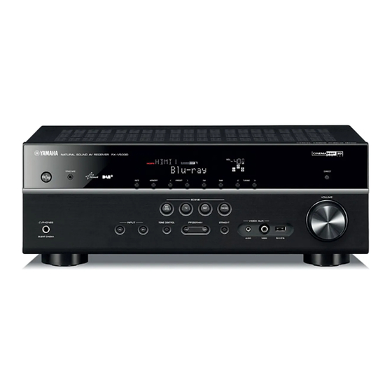
Page 3: Front Panels
RX-V475/HTR-4066/RX-V500D ■ FRONT PANELS RX-V475 U, C, R, T, K, A, B, G, F, L, S, H models J model HTR-4066 RX-V500D... -
Page 4: Rear Panels
RX-V475/HTR-4066/RX-V500D ■ REAR PANELS RX-V475 (U, C models) RX-V475 (R, S models) RX-V475 (T model) - Page 5 RX-V475/HTR-4066/RX-V500D RX-V475 (K model) RX-V475 (A model) RX-V475 (B, G, F models)
- Page 6 RX-V475/HTR-4066/RX-V500D RX-V475 (L, H models) RX-V475 (J model) HTR-4066 (U model)
- Page 7 RX-V475/HTR-4066/RX-V500D HTR-4066 (R model) HTR-4066 (T model) HTR-4066 (K model)
- Page 8 RX-V475/HTR-4066/RX-V500D HTR-4066 (A model) HTR-4066 (B, G, F models) HTR-4066 (L model)
- Page 9 RX-V475/HTR-4066/RX-V500D RX-V500D (A model) RX-V500D (B, G models)
-
Page 10: Remote Control Panels
RX-V475/HTR-4066/RX-V500D ■ REMOTE CONTROL PANELS RAV494 RAV495 RX-V475 / HTR-4066 RX-V500D Remote control sheet (T model) -
Page 11: Specifications
RX-V475/HTR-4066/RX-V500D ■ SPECIFICATIONS / 参考仕様 ■ Audio Section / オーディオ部 Rated Output Power (Power Amp. Section) / Signal to Noise Ratio / 信号対雑音比 (IHF-A network) 定格出力(パワーアンプ部) AV5, etc. (PURE DIRECT) to SP OUT (Input shorted 250 mV) ................100 dB or more (1 kHz, 0.9 % THD) - Page 12 ..................Loop antenna Remote control ................x 1 Battery (R03, AAA, UM-4) .............x 2 ■ DAB Tuner Section [RX-V500D] FM antenna (1.4 m) (RX-V475/HTR-4066) ........x 1 Tuning Range AM antenna (1 m) (RX-V475/HTR-4066) ........x 1 ..............174 to 240 MHz (Band III) DAB/FM antenna (1.6 m) (RX-V500D) ..........x 1...
- Page 13 (2") “x.v.Color” is a trademark of Sony Corporation. 「x.v.Color」は、ソニー株式会社の商標です。 Front view “SILENT CINEMA” is a trademark of Yamaha Corporation. 「サイレントシネマ™ SILENT CINEMA ™」はヤマハ株式会社の登録商標です。 435 (17-1/8") DLNA™ and DLNA CERTIFIED™ are trademarks or registered trademarks of Digital Living Network Alliance. All rights reserved. Unauthorized use is strictly prohibited.
- Page 14 RX-V475/HTR-4066/RX-V500D • SET MENU TABLE MAIN SUB-MENU PARAMETER VALUE [INITIAL VALUE] MENU Speaker Configuration Subwoofer [Use] / None Front [Small] / Large Center [Small] / Large / None Surround [Small] / Large / None Crossover 40 Hz / 60 Hz / [80 Hz] / 90 Hz / 100Hz / 110 Hz / 120 Hz / 160 Hz /...
- Page 15 RX-V475/HTR-4066/RX-V500D MAIN SUB-MENU PARAMETER VALUE [INITIAL VALUE] MENU HDMI Configuration HDMI Control [Off] / On (U, C, R, T, K, A, B, G, F, L, S, H models) Off / [On] (J model) Audio Output Off / [On] HDMI OUT (TV) [Off] / On * This setting is available only when “HDMI Control”...
- Page 16 RX-V475/HTR-4066/RX-V500D MAIN SUB-MENU PARAMETER VALUE [INITIAL VALUE] MENU Function Input Rename Input sources: HDMI1 / HDMI2 / HDMI3 / HDMI4 / HDMI5 / AV1 / AV2 / AV3 / AV4 / AV5 / AV6 / AUDIO / USB / V-AUX...
-
Page 17: Internal View
Top view OPERATION (2) P.C.B. MAIN (4) P.C.B. (R, S models) MAIN (1) P.C.B. DIGITAL P.C.B. OPERATION (8) P.C.B. AM/FM TUNER (RX-V475/HTR-4066) DAB P.C.B. (RX-V500D) OPERATION (3) P.C.B. MAIN (3) P.C.B. MAIN (2) P.C.B. MAIN (5) P.C.B. OPERATION (4) P.C.B. -
Page 18: Disassembly Procedures
RX-V475/HTR-4066/RX-V500D ■ DISASSEMBLY PROCEDURES / 分解手順 (Remove parts in the order as numbered.) (番号順に部品を外してください。 ) Disconnect the power cable from the AC outlet. AC 電源コンセントから、電源コードを抜いてください。 1. Removal of Top Cover 1. トップカバーの外し方 a. Remove 4 screws ( ① ) and 5 screws ( ② ). (Fig. 1) a. - Page 19 RX-V475/HTR-4066/RX-V500D 3. Removal of DIGITAL P.C.B. 3. DIGITAL P.C.B. の外し方 a. Remove 2 screws ( ④ ) and 6 screws ( ⑤ ). (Fig. 3) a. ④ のネジ 2 本、⑤ のネジ 6 本を外します。 (Fig. 3) b. Remove 2 screws ( ⑥ ). (Fig. 2) b.
- Page 20 RX-V475/HTR-4066/RX-V500D When checking the MAIN (1) P.C.B.: MAIN(1)P.C.B. をチェックする場合には: • Place the P.C.B.s (with rear panel) upright. (Fig. 4) ・ リアパネルと一緒に P.C.B. を立ち上げて置きます。 (Fig. 4) • Connect the heatsink and rear panel to the chassis with a ground lead or the like. (Fig. 4) ・...
- Page 21 RX-V475/HTR-4066/RX-V500D When checking the DIGITAL P.C.B.: DIGITAL P.C.B. をチェックする場合には: • Put the rubber sheet and cloth over this unit, and ・ 本機の上にゴムシートと布を敷き、その上に DIGITAL place the DIGITAL P.C.B. on them. (Fig. 5) P.C.B. を置きます。 (Fig. 5) • Connect ST951 on DIGITAL P.C.B. to the chassis ・...
-
Page 22: Updating Firmware
● Required Tools ● 必要なツール • USB storage device ・ USB フラッシュメモリー • Firmware ・ ファームウェア RX-V475/HTR-4066: R0326-xxxx.bin RX-V475: R0326-xxxx.bin RX-V500D: R0330-xxxx.bin ● Preparation ● 準備 1. Download the latest firmware from the specified 1. 指定のダウンロード先から、最新のファームウェ download source to the folder of the PC. - Page 23 RX-V475/HTR-4066/RX-V500D ● Operation Procedures ● 操作手順 1. Insert the USB storage device to the USB jack. 1. USB 端子に USB フラッシュメモリーを差し込みま (Fig. 1) す。 (Fig. 1) 2. While pressing the “INFO” key, connect the power INFO キーを押しながら、電源コードを AC コン cable to the AC outlet. (Fig. 1) セントに接続します。...
- Page 24 RX-V475/HTR-4066/RX-V500D ■ SELF-DIAGNOSTIC FUNCTION / ダイアグ(自己診断機能) This unit has self-diagnostic functions that are intended 本機には、検査、測定、不良個所の発見を目的にしたダ for inspection, measurement and location of faulty point. イアグ(自己診断機能)があります。 There are 27 main menu items, each of which has sub- ダイアグには 27 個のメインメニューがあり、そのそれぞ menu items.
- Page 25 RX-V475/HTR-4066/RX-V500D Main menu Sub-menu C: Communication system / 通信・バスライン系 DIGITAL PCB CHECK MCPU OSD OSD HDMI VIDEO I/F Not for service / サービスでは使用しません BUS DIR BUS DSP EEPROM TUNER HDMI INFO HDMI MODEL NAME HDMI PRODUCT ID Not for service / サービスでは使用しません...
- Page 26 RX-V475/HTR-4066/RX-V500D Main menu Sub-menu S: System and version system / システム・バージョン系 FIRMWARE UPDATE DSP FIRMWARE UPDATE Not for service / サービスでは使用しません SET INFORMATION INITIAL DISPLAY MODEL/DESTINATION FACTORY PRESET PRESET INHIBIT PRESET RESERVED ROM VERSION/CHECKSUM SYSTEM VERSION MICROPROCESSOR VERSION MICROPROCESSOR CHECKSUM...
- Page 27 RX-V475/HTR-4066/RX-V500D ● Starting Self-Diagnostic Function ● ダイアグの起動 While pressing the “TONE CONTROL” and “INFO” keys, TONE CONTROL と INFO キーを押しながら (電源) press the “ ” (Power) key to turn on the power, and release キーを押して電源を入れた後、2 つのキーを放します。 those 2 keys. ダイアグが起動します。...
- Page 28 RX-V475/HTR-4066/RX-V500D ● Canceling Self-Diagnostic Function ● ダイアグの解除 Before canceling self-diagnostic function, execute ダイアグを解除する前に、 S3. FACTORY PRESET メ setting for “S3. FACTORY PRESET” menu. (Memory ニュー(メモリーの初期化禁止/またはメモリーの initialization inhibited or Memory initialized). 初期化)の設定をします。 In order to keep the user memory preserved, be ※...
- Page 29 RX-V475/HTR-4066/RX-V500D 2. When the protection function worked to turn 2. プロテクションが働いて電源が切れた場合: off the power: The information of protection function which worked at そのときに働いたプロテクションの情報が表示され that time is displayed. Then “A1-1. DSP MARGIN” is ます。数秒後、 A1-1. DSP MARGIN が表示されます。 displayed in a few seconds.
- Page 30 RX-V475/HTR-4066/RX-V500D 2-2. When the protection function worked due to 2-2. DC 出力異常によりプロテクションが働いた場合 abnormal DC output. H: Displayed when the voltage is HIGHER than upper limit 電圧が上限値より高い場合に表示されます L: Displayed when the voltage is LOWER than lower limit 電圧が下限値より低い場合に表示されます D C P R T : x x x H xxx: A/D conversion value of voltage at the moment when the protection function worked (Reference voltage: 3.3 V=255)
- Page 31 RX-V475/HTR-4066/RX-V500D 2-4. When the protection function worked due to 2-4. ヒートシンクの異常温度によりプロテクション excessive heatsink temperature. が働いた場合 H: Displayed when the voltage is HIGHER than upper limit 電圧が上限値より高い場合に表示されます L: Displayed when the voltage is LOWER than lower limit 電圧が下限値より低い場合に表示されます T M P x P R T : x x x L xxx: A/D conversion value of voltage at the moment when the protection function worked (Reference voltage: 3.3 V=255)
- Page 32 RX-V475/HTR-4066/RX-V500D ● Operation procedure of Main menu ● メインメニューとサブメニューの操作 and Sub-menu There are 27 main menu items, each of which has sub- ダイアグには 27 個のメインメニューがあり、そのそれぞ menu items. れにサブメニューがあります。 Main menu selection メインメニューの選択 Select the main menu using “SCENE TV” (forward) and SCENE TV (順送り)...
- Page 33 RX-V475/HTR-4066/RX-V500D ● Details of Self-Diagnostic Function ● ダイアグメニュー詳細 menu A1. DSP AUDIO A1. DSP AUDIO This menu is used to check audio signal route via DSP. DSP を経由する音声信号の経路をチェックします。 A1-1. DSP MARGIN A1-1. DSP MARGIN The audio signal is output including the head 音声信号が...
- Page 34 RX-V475/HTR-4066/RX-V500D A1-5. DSP FULL SURROUND BACK A1-5. DSP FULL SURROUND BACK Not for service. サービスでは使用しません。 A 1 - 5 D S P F U L L S B A1-6. DSP FULL SUBWOOFER A1-6. DSP FULL SUBWOOFER The audio signal is output to only SUBWOOFER 音声信号がヘッドマージンを含まず、デジタ...
- Page 35 RX-V475/HTR-4066/RX-V500D A3. HDMI AUDIO A3. HDMI AUDIO This menu is used to check the route of audio signal HDMI IN/OUT 端子へ入力された音声信号の経路を input to HDMI IN/OUT jack. チェックします。 * Before check using “A3-2. ARC” menu, be sure to ※ A3-2. ARC メニューでのチェックの前に、あらか...
- Page 36 RX-V475/HTR-4066/RX-V500D A5. MIC CHECK A5. MIC CHECK A5-1. MIC ROUTE CHECK A5-1. MIC ROUTE CHECK The audio signal input to the YPAO MIC jack is YPAO マイク端子へ入力された音声信号が A/D output to FRONT L channels via A/D-D/A. − D/A 経由で FRONT L チャンネルへ出力され...
- Page 37 RX-V475/HTR-4066/RX-V500D A8. MANUAL TEST A8. MANUAL TEST The test noise generated by built-in noise generator DSP に内蔵されたノイズジェネレータによって生成 in DSP is output to the channels specified by the sub- されたテストノイズが、サブメニューで指定したチャ menu. ンネルへ出力されます。 Test noise / テストノイズ 30 Hz to 80 Hz for SUBWOOFER / SUBWOOFER 用...
- Page 38 RX-V475/HTR-4066/RX-V500D D1. FL CHECK D1. FL CHECK This menu is used to check operation of the FL display. FL 表示の動作をチェックします。 FL display / FL 表示 D1-1. INITIAL DISPLAY / 初期表示 D1-2. ALL SEGMENT OFF / 全セグメント消灯 D1-3. ALL SEGMENT ON / 全セグメント点灯...
- Page 39 RX-V475/HTR-4066/RX-V500D U1. USB U1. USB This menu is used to check the audio signal route from USB フラッシュメモリーからの音声信号の経路をチェッ クします。 USB storage device. U1-1. USB FRONT 1 TRACK U1-1. USB FRONT 1 TRACK The 1st music file stored in the USB storage USB 端子に接続された...
- Page 40 RX-V475/HTR-4066/RX-V500D N1. NETWORK N1. NETWORK This menu is used to check functions related to ネットワークに関連する機能をチェックします。 NETWORK. ブ ロ ー ド バ ン ド ル ー タ ー の LAN ポ ー ト と 本 機 の Connect between LAN port of broadband router and NETWORK 端子をネットワークケーブルで接続しま...
- Page 41 RX-V475/HTR-4066/RX-V500D N1-5. LINE NOISE 10 MDI N1-5. LINE NOISE 10 MDI Not for service. サービスでは使用しません。 N 1 - 5 L N M D I 1 0 N1-6. LINE NOISE 10 MDIX N1-6. LINE NOISE 10 MDIX Not for service. サービスでは使用しません。...
- Page 42 RX-V475/HTR-4066/RX-V500D C1. DIGITAL P.C.B. CHECK C1. DIGITAL P.C.B. CHECK This menu is used to check the communication and DIGITAL P.C.B. 上の各デバイス間の通信とバスライン bus line connection between devices on DIGITAL 接続をチェックします。 P.C.B. C1-1. ALL C1-1. ALL The total detection result of sub-menus from サブメニュー...
- Page 43 OK: No error detected / 不良検出なし NG: An error is detected / 不良検出あり Checking / チェック中 C1-8. TUNER C1-8. TUNER The AM/FM (RX-V475/HTR-4066) / DAB (RX- AM/FM TUNER の I2C(Inter integrated circuit) V500D) TUNER I2C (Inter integrated circuit) バスライン接続をチェックします。 bus line connection is checked.
- Page 44 RX-V475/HTR-4066/RX-V500D C2. HDMI INFORMATION C2. HDMI INFORMATION This menu is used to display information about HDMI. HDMI に関する情報が表示されます。 C2-1. HDMI MODEL NAME C2-1. HDMI MODEL NAME The model name written to HDMI IC is HDMI IC に書き込まれているモデル名が表示 displayed. されます。 C 2 - 1...
- Page 45 RX-V475/HTR-4066/RX-V500D C3. NETWORK IC CHECK C3. NETWORK IC CHECK This menu is used to check the communication and bus ネットワークに関連する各デバイス間の通信とバス line connection between devices related to network. ラインの接続をチェックします。 C3-1. ALL C3-1. ALL The total detection result of sub-menus from サブメニュー C3-2 ∼ C3-4 の総合判定結果が...
- Page 46 RX-V475/HTR-4066/RX-V500D V1. ANALOG VIDEO CHECK V1. ANALOG VIDEO CHECK This menu is used to check the analog video signal アナログ映像信号の経路をチェックします。 route. V1-1. ANALOG BYPASS V1-1. ANALOG BYPASS The video signal is output as shown below. 映像信号が以下のように出力されます。 V 1 - 1...
- Page 47 RX-V475/HTR-4066/RX-V500D V2. DIGITAL VIDEO CHECK V2. DIGITAL VIDEO CHECK This menu is used to check the digital video signal デジタル映像信号の経路をチェックします。 route. V2-1. HDMI REPEAT V2-1. HDMI REPEAT The video/audio signals input to HDMI IN jack HDMI IN 端子へ入力された映像信号と音声信 are output to HDMI OUT jack.
- Page 48 RX-V475/HTR-4066/RX-V500D V2-2. OSD (On-Screen Display) VIDEO OUT V2-2. OSD(On-Screen Display)VIDEO OUT The “OSD CHECK” screen is output to HDMI OSD CHECK 画面が HDMI OUT 端子へ出力さ OUT jack. れます。 V 2 - 2 O S D - V I D E O O U T...
- Page 49 RX-V475/HTR-4066/RX-V500D R1. DAB (RX-V500D model) R1. DAB(RX-V500D model) This menu is used to display the DAB module サービスでは使用しません。 information. R 1 - 1 R 1 - 2 R1-1. SIGNAL QUALITY I n v a l i d i t y I n v a l i d i t y Not for service.
- Page 50 RX-V475/HTR-4066/RX-V500D P1-2. PS P1-2. PS Power supply voltage (PS) protection detection. 電源電圧(PS)プロテクションの検出 The voltage at 126 pin (PS1_PRT)/107 pin (PS2_ IC21 の 126 ピン (PS1_PRT) / 107 ピン (PS2_ PRT)/106 pin (PS3_PRT) of IC21 are displayed. PRT)/ 106 ピン(PS3_PRT)の電圧が表示さ れます。...
- Page 51 RX-V475/HTR-4066/RX-V500D P1-4. OUTPUT LEVEL P1-4. OUTPUT LEVEL Output level of speaker output is detected. スピーカー出力の出力レベルの検出 The voltage at 121 pin (LMT_0LV) of IC21 is IC21 の 121 ピン(AMP_OLV)の電圧が表示さ displayed. れます。 (Reference voltage: 3.3 V=255) (基準電圧:3.3 V=255) P 1 - 4 O U T L V L : 2 5 5 P1-5.
- Page 52 RX-V475/HTR-4066/RX-V500D P1-7. KEY P1-7. KEY Panel key is detected. パネルキーの検出 When the A/D conversion value of the panel パネルキーの A/D 値が規定範囲から外れると、 key becomes out of the specified range, normal 正常な動きをしません。 operation will not be available. 下表をご覧になり、各キーの分圧抵抗の定数、 In that case, check the constant of voltage dividing ハンダ不良等の確認をしてください。...
- Page 53 RX-V475/HTR-4066/RX-V500D P2. PROTECTION HISTORY P2. PROTECTION HISTORY This menu is used to display the history of protection プロテクション履歴が表示されます。 function. 履歴 1 ∼ 4 には、そのそれぞれにプロテクション動 In the history 1 to 4, the setting information for 作時の設定情報が保存されます。 operation of each protection function will be stored.
- Page 54 RX-V475/HTR-4066/RX-V500D T1. TROUBLE SHOOTING INFORMATION T1. TROUBLE SHOOTING INFORMATION This menu is used to display the operating time and 本機の動作時間、動作回数が表示されます。 operation frequency of this unit. ※ ダイアグ中の動作時間、動作回数は保存されませ The operating time and operation frequency during ん。 the self-diagnostic function mode will not be stored.
- Page 55 Destination / 仕向け先 U / C / R (R, S) / T / K / A / G (B, G, F) / L (L, H) / J Model name / モデル名 V475 : RX-V475 H4066 : HTR-4066 V500D : RX-V500D S3.
- Page 56 RX-V475/HTR-4066/RX-V500D S4. ROM VERSION/CHECKSUM S4. ROM VERSION/CHECKSUM The firmware version and checksum values are ファームウェアのバージョン、チェックサムが表示 displayed. されます。 The checksum is obtained by adding the data at every チェックサムは、データを 8 ビットごとに加算して 8-bit and expressing the result as a hexadecimal いき、16 進数で表記したものです。...
- Page 57 U - S u m : - - - - Not for service. サービスでは使用しません。 S5. SOFT SWITCH (RX-V475/HTR-4066 models) S5. SOFT SWITCH This menu is used to write the model name to the モデル名をバックアップ IC (EEPROM : DIGITAL P.C.B. の...
- Page 58 U / C / R (R, S) / T / K / A / G (B, G, F) / L, H / J Not for service. / サービスでは使用しません。 Model name / モデル名 V4 (RX-V475) / H4 (HTR-4066) / D5 (RX-V500D) S6-2. VERIFY S6-2. VERIFY Not for service.
-
Page 59: Power Amplifier Adjustment
RX-V475/HTR-4066/RX-V500D ■ POWER AMPLIFIER ADJUSTMENT / パワーアンプ調整 1. Right after power is turned on, confirm that the voltage 1. 電源投入直後、 R2152 (SURROUND Rch) 、 R2149 (FRONT across the terminals of R2152 (SURROUND Rch), R2149 Rch) 、R2151 (CENTER) 、R2150 (FRONT Lch) 、R2153 (FRONT Rch), R2151 (CENTER), R2150 (FRONT Lch) (SURROUND Lch)の端子間電圧を測定し、0.1 mV から... -
Page 60: Display Data
RX-V475/HTR-4066/RX-V500D ■ DISPLAY DATA ● V4001 : 18-MT-11GNAK (OPERATION P.C.B.) PATTERN AREA ● PIN CONNECTION Pin No. 68 67 Connection F2 NX 29 28 Pin No. Connection Note : 1) F1, F2 ..Filament pin 2) NP ..No pin 3) NX .. - Page 61 RX-V475/HTR-4066/RX-V500D ● ANODE CONNECTION 1G-14G –...
- Page 62 RX-V475/HTR-4066/RX-V500D ■ IC DATA IC1: SII9573CTUC (DIGITAL P.C.B.) HDMI port processors * No replacement part available. / サービス部品供給なし Always-On CEC A0 Section CEC A1 CEC Interface CEC Interface CBUS/ Mobile HD Controller 1 Controller 0 Control CBUS0 78,82,86,90,94,99 Serial Ports...
- Page 63 RX-V475/HTR-4066/RX-V500D HDMI Receiver and MHL Port Pins HDMI Transmitter Port Pins Function Function Type Detail of Function Type Detail of Function Name Name R0X0- T0X0- R0X0+ T0X0+ HDMI transmitter Port 0 TMDS output data pairs. R0X1- T0X1- HDMI receiver Port 0 TMDS input data...
- Page 64 RX-V475/HTR-4066/RX-V500D Audio Pins SPI Interface Pins Function Function Type Detail of Function Type Detail of Function Name Name WS0_OUT/ Main port I2S word select output/DSD Input/ LVTTL Output SS/GPIO2 LVTTL SPI slave select/programmable GPIO 2. data right bit 0. Output...
- Page 65 RX-V475/HTR-4066/RX-V500D System Switching Pins Function Name Type Detail of Function DSDA0 DSDA1 DDC I2C data for respective HDMI receiver port. DSDA2 LVTTL Schmitt Open Input/Output drain 5 V tolerant DSDA3 These signals are true open drain, and do not pull to ground when power is not applied to the device.
- Page 66 RX-V475/HTR-4066/RX-V500D Control Pins Function Name Type Detail of Function Local configuration/status I2C clock. Schmitt Open drain 5 CSCL Input V tolerant Chip configuration/status is accessed via this I2C port. This pin is true open drain, so it does not pull to ground if power is not applied.
- Page 67 RX-V475/HTR-4066/RX-V500D Power and Ground Pins Function Name Type Detail of Function AVDD33 Power 3.3 V TMDS core VDD. IOVCC33 Power 3.3 V I/O VCC. Local power from system. SBVCC5 Power 5.0 V This pin requires a 10 ohms series resistor.
- Page 68 RX-V475/HTR-4066/RX-V500D IC41: D70YE101BRFP266 (DIGITAL P.C.B.) Decoder/Post processor * No replacement part available. / サービス部品供給なし Program/Data JTAG EMU 256K Bytes McASP0 Data 16 Serializes Program/Data C67x+CPU ROM Page1 256K Bytes Memory Data Controller Program/Data McASP1 ROM Page2 6 Serializes 256K Bytes...
- Page 69 RX-V475/HTR-4066/RX-V500D Function Name Detail of Function (P.C.B.) AHCLKX0/AHCLKX2 McASP0 and McASP2 transmit master clock AMUTE0 McASP0 mute output AMUTE1 McASP1 mute output AHCLKX1 McASP1 transmit master clock ACLKX1 McASP1 transmit bit clock CVDD ACLKR1 McASP1 receive bit clock DVDD AFSX1...
- Page 70 RX-V475/HTR-4066/RX-V500D Function Name Detail of Function (P.C.B.) EM_D[1] EMIF data bus [lower 16-bits] EM_D[0] EMIF data bus [lower 16-bits] CVDD EM_D[15] EMIF data bus [lower 16-bits] EM_D[14] EMIF data bus [lower 16-Bits] CVDD EM_D[13] EMIF data bus [lower 16-Bits] EM_D[12]...
- Page 71 RX-V475/HTR-4066/RX-V500D Function Name Detail of Function (P.C.B.) 101 CVDD 102 NC Asynchronous memory read/not write 103 DVDD 104 EM_OE SDRAM output enable 105 SPI0_ENA/I2C1_SDA SPI0 enable (ready) or I2c1 serial data 106 VSS 107 SPI0_ENA/I2C1_SCL SPI0 enable (ready) or I2c1 serial clock...
- Page 72 RX-V475/HTR-4066/RX-V500D IC951: DM860A (DIGITAL P.C.B.) Network microprocessor * No replacement part available. / サービス部品供給なし General Purpose Security Engine Timing Engine on-chip RAM RESET, BOOT_SEL CLOCKS Reset, Boot, OTP 2 PLLs, 3 DCOs 64 kBytes master AV0 Port slave 4xAudio, 1xVideo...
- Page 73 RX-V475/HTR-4066/RX-V500D AV-Port 0 Pin No. Function Name Detail of Function Audio/video data. AV0DATA[3:0] Several formats are supported. Video data, together with AV0DATA[3:0]: AV0DATA[3:0] = video[3:0] AV1DATA[3:0] AV1DATA[3:0] = video[7:4] Data clock. Depending on the AV-Port 0 configuration, this clock is a bit- or byte-clock which is used to AV0CLK transmit or receive the AV0DATA[*] synchronously.
- Page 74 RX-V475/HTR-4066/RX-V500D Serial Peripheral Interface (SPI) Pin No. Function Name Detail of Function SPIDIN SPI data receive. SPIDOUT SPI data transmit. SPICLK SPI clock. Multi-master mode: Chip-select input (used to detect bus conflict). SPINCS0 Master only mode: Chip-select 1 output. Slave mode: Chip-select input.
- Page 75 RX-V475/HTR-4066/RX-V500D Pin No. Function Name Detail of Function Chip select signals. The active memory range for NCS[n] (active low) can be configured. • NCS[0] supports SRAM, can be used for booting. NCS[3:0] • NCS[1] supports SDRAM or SRAM. • NCS[2] supports SRAM.
- Page 76 RX-V475/HTR-4066/RX-V500D USB 2.0 OTG Pin No. Function Name Detail of Function USBD+ Positive data line that is connected to the serial USB cable. USBD– Negative data line that is connected to the serial USB cable. USBID USB ID pin of mini-AB receptacle.
- Page 77 RX-V475/HTR-4066/RX-V500D SSM Interface Pin No. Function Name Detail of Function SSMD[7:0] Data lines. SSMCLK Clock output. SSMCMD Command output. SSMCP Card power input (high = off). SSMWP Write protect input (low = protect). External PLL Pins Pin No. Function Name Detail of Function External oscillator inputs, typically coming from an external VCO.
- Page 78 RX-V475/HTR-4066/RX-V500D Power Supply Pins Pin No. Function Name Detail of Function Pin No. Function Name Detail of Function VDD33 I/O power supply (+3.3 V). Ground (0 V). VDD33USB Power supply (+3.3 V) for USB interface. Ground (0 V). VSS33USB VDD33PLL Power supply (+3.3V) for PLL.
- Page 79 RX-V475/HTR-4066/RX-V500D IC225: R5F3651TNFC (DIGITAL P.C.B.) Microprocessor * No replacement part available. / サービス部品供給なし Port P0 Port P1 Port P2 Port P3 Port P4 Port P5 Port P12 Port P13 VCC2 ports Internal peripheral functions System clock generator UART or clock synchronous serial I/O...
- Page 80 RX-V475/HTR-4066/RX-V500D Function Name Port Name Detail of Function (P.C.B.) VREF VREF AD standard voltage AVCC AVCC Microprocessor power supply SIN4 EEP_MISO EEPROM / Expansion Flash synchronization data input SOUT4 EX_MOSI FL driver / EEPROM / Expansion Flash synchronization data input...
- Page 81 RX-V475/HTR-4066/RX-V500D Function Name Port Name Detail of Function (P.C.B.) P5_4 HP_N_DET Headphone detection / L: Headphone detected P13_3 HPRY Headphone relay control P13_2 SPRY_SB_BA Speaker relay control (Surround back and Bi-Amp) P13_1 (no use) P13_0 SPRY_5CH Speaker relay control (Front / Center / Surround) / H: Relay ON...
- Page 82 RX-V475/HTR-4066/RX-V500D Function Name Port Name Detail of Function (P.C.B.) 104 P0_7 DAC_N_CS DAC chip select 105 P0_6 NCPU_AMUTE NET audio mute demand 106 AN0_5 PS3_PRT PS protection detection 3 107 AN0_4 PS2_PRT PS protection detection 2 108 AN0_3 L3_DET D terminal L3 detection...
-
Page 83: Pin Connection Diagrams
RX-V475/HTR-4066/RX-V500D ■ PIN CONNECTION DIAGRAMS • ICs • ICs A3V56S30FTP-G6 BA4560F-E2 D70YE101BRFP266 DM860A-AQE STR2A153 TC74LCX245FT TC74VHCU04FT TC7MBL3257CFK TC7WH125FK W25Q16CVSSIG TL431ACLPR TC7WH126FK BD7542F-E2 1: CATHODE 2: ANODE 3: REF 74LVC08APW BD3473KS2 • Diodes BD9328FJ 1N4003S 1SS355VMTE-17 DBL155G RB051L-40 RB215T-90 RB500V-40 RF101L2STE25... - Page 84 RX-V475/HTR-4066/RX-V500D ■ BLOCK DIAGRAMS 20-27 HDMI IN 1 HDMI 28-35 HDMI IN 2 HDMI_CEC Receiver/Transmitter 39-44 HDMI IN 3 SII9573CTUC FLASH ROM OSD_MOSI/OSD_MISO/OSD_CLK OSD_N_CS W25Q16CVSSIG 47-54 HDMI IN 4 16Mb 57-64 HDMI IN 5 /MHL HDMI OUT IC953 IC952 IC954...
- Page 85 RX-V475/HTR-4066/RX-V500D Power Supply Section Block Diagram Speaker Impedance relay IC25 +5.5V +3.3M Microprocessor (IC21)/Standby LED/Remote/key input Power +3.3M Power Amplifier Transformer RY206 IC24 D2046 C2084 +3.3S Control circuits around Microprocessor +3.3S +3.3S_PON IC67 C2085 +3.3H HDMI (IC1) +3.3H +3.3D RY206...
- Page 86 RX-V475/HTR-4066/RX-V500D ■ WIRING DIAGRAMS • OVERALL ASSEMBLY RX-V475/ RX-V500D to AM/FM TUNER HTR-4066 20 mm Contact side OPERATION (3) (3/4") AM/FM TUNER to DAB (CB502) Bend W2006 Contact side OPERATION (2) W5002 CB502 B505 PN501 DIGITAL to DIGITAL CB545 PN21...
- Page 87 RX-V475/HTR-4066/RX-V500D • AMP UNIT CB522 OPEARTION (4) CB525 Fix the wires by style-pin (PN201) not to approach Q2015/2018/ CB477 2019/2020/2021. Fix the wires by PN522 CB521 CB522 PN522 CB524 CB523 MAIN (1) PN205 W2013A W2012A Check whether W2005 is passing under PN201 2 wires as shown in the figure.
- Page 88 RX-V475/HTR-4066/RX-V500D RX-V475/HTR-4066 RX-V500D ■ PRINTED CIRCUIT BOARDS • Semiconductor Location Ref no. Location Ref no. Location Ref no. Location Ref no. Location Ref no. Location Ref no. Location Ref no. Location Ref no. Location Ref no. Location D205 IC22 IC41...
- Page 89 RX-V475/HTR-4066/RX-V500D RX-V475/HTR-4066 RX-V500D DIGITAL (Side B) IC954 • Semiconductor Location Ref no. Location D101 D102 IC42 IC42 IC45 IC71 IC954 Q202 Q203 Q204 Q205 Q206 RX-V500D...
- Page 90 RX-V475/HTR-4066/RX-V500D RX-V475/HTR-4066 RX-V500D OPERATION (1) (Side A) DIGITAL (CB21) IN_RD Remote control sensor IN_RC FLD_N_RST FLD_N_CS FLD_SCK FLD_MOSI MIC_N_DET PSW_N_DET KEY1 KEY2 REM_IN OPERATION (4) +3.3DSP VOL_RB (CB525) DGND VOL_RA +3.3M STBY_LED VAUX VAUXE +12V -12V AUXR AUXL AUXE TUNING...
- Page 91 RX-V475/HTR-4066/RX-V500D RX-V475/HTR-4066 RX-V500D OPERATION (1) (Side B) 49 48 IC401 16 17 • Semiconductor Location Ref no. Location D4003 D4004 D4005 D4006 D4007 D4008 D4013 D4014 D4015 D4016 IC401 Q4001 Q4002 Q4003 Q4004...
- Page 92 RX-V475/HTR-4066/RX-V500D RX-V475/HTR-4066 RX-V500D OPERATION (2) OPERATION (3) (Side A) (Side A) MAIN (5) (CB373) DIGITAL (CB64) OPERATION (4) W5401 (CB523) DIGITAL (CB24) CB505 DIGITAL DEST (CB91) CPU_N_RST ACPWR_DET DGND +3.3M L3_DET VID_SDA VID_SCL W5002 5 k-ohms 10 W MONITOR OUT...
- Page 93 RX-V475/HTR-4066/RX-V500D RX-V475/HTR-4066 RX-V500D OPERATION (2) OPERATION (3) (Side B) (Side B) IC502 IC501 • Semiconductor Location Ref no. Location Ref no. Location D5402 D5412 D5403 D5413 D5405 D5414 IC501 D5406 D5407 IC502 D5408 Q5401 D5409 Q5402 D5410 Q5403 D5411...
- Page 94 RX-V475/HTR-4066/RX-V500D RX-V475/HTR-4066 RX-V500D OPERATION (4) (Side A) DIGITAL (CB25) POWER TRANSFORMER MAIN (1) OPERATION (3) (CB207) (CB505) CB522 CB523 CB524 CB521 • Semiconductor Location Ref no. Location CB525 D4504 D5204 OPERATION (1) D5206 (CB403) IC521 IC522 IC523 IC524 IC525 Q5201...
- Page 95 RX-V475/HTR-4066/RX-V500D RX-V475/HTR-4066 RX-V500D OPERATION (4) (Side B) RX-V475/HTR-4066 • Semiconductor Location Ref no. Location D4501 D4502 D4503 D5201 D5202 D5205 D5207 D5208 IC471 Q4501 Q5202 Q5203 R, S models R, T, K, A, B, G, F, L, S, H, J models...
- Page 96 RX-V475/HTR-4066/RX-V500D RX-V475/HTR-4066 RX-V500D OPERATION (7) OPERATION (8) OPERATION (9) (Side A) (Side A) (Side A) PHONES SILENT CINEMA JK476 DIGITAL (CB65) W4761 to chassis W5301 CB532 HP_N_DET MAIN (1) (W2005) DC OUT (USB)
- Page 97 RX-V475/HTR-4066/RX-V500D RX-V475/HTR-4066 RX-V500D OPERATION (7) OPERATION (8) OPERATION (9) (Side B) (Side B) (Side B) • Semiconductor Location Ref no. Location D4761 D4762...
- Page 98 RX-V475/HTR-4066/RX-V500D RX-V475/HTR-4066 RX-V500D Safety measures • Semiconductor Location • Some internal parts in this product contain high voltages and are dangerous. Be sure to take safety measures during servicing, such Ref no. Location Ref no. Location Ref no. Location as wearing insulating gloves.
- Page 99 RX-V475/HTR-4066/RX-V500D RX-V475/HTR-4066 RX-V500D MAIN (1) (Side B) • Semiconductor Location Ref no. Location Ref no. Location IC203 D2051 D2003 D2004 IC201 D2005 IC202 D2006 IC203 41 40 D2007 Q2001 IC202 D2008 Q2002 D2009 Q2003 IC201 D2010 Q2004 D2011 Q2008 20 21...
- Page 100 RX-V475/HTR-4066/RX-V500D RX-V475/HTR-4066 RX-V500D MAIN (2) MAIN (3) (Side A) (Side A) NETL DA-FR NETE NETR NETL DA-FL NETE DA-SR DAFR NETR DA-SL DAFL IC271 DA-SW +12V DASR DA-C DASL AV4_D DA-SBR AV3_D DGND DA-SBL DASW AV4_D DGND AV2_D AV3_D AV1_D...
- Page 101 RX-V475/HTR-4066/RX-V500D RX-V475/HTR-4066 RX-V500D MAIN (2) MAIN (3) (Side B) (Side B) IC251 IC252 IC253 IC254 • Semiconductor Location Ref no. Location D2701 IC251 IC252 IC253 MAIN (4) MAIN (5) (Side B) (Side B) R, S models...
- Page 102 RX-V475/HTR-4066/RX-V500D RX-V500D (Side A) (Side B) LOUT/SPDIF DAB MODULE ROUT TUNE_GND TUNE/NC SCLK SDIO /RST IC501 DIGITAL (CB26) • Semiconductor Location Ref no. Location D501 IC501...
- Page 103 RX-V475/HTR-4066/RX-V500D SCHEMATIC DIAGRAMS RX-V475/HTR-4066 RX-V500D DIGITAL 1/5 HDMI 5 HDMI 4 HDMI 3 HDMI 2 HDMI 1 HDMI OUT (BD/DVD) H D M I O U T H D M I I N - 5 / M H L I N...
- Page 104 RX-V475/HTR-4066/RX-V500D RX-V475/HTR-4066 RX-V500D DIGITAL 2/5 to AM/FM TUNER (RX-V475/HTR-4066) Page 109 Page 108 Page 111 Page 109 Page 109 Page 113 to OPERATION (3)_CB504 to OPERATION (1)_CB402 to MAIN (1)_CB211 to OPERATION (2)_CB545 to OPERATION (4)_CB521 to DAB_CB502 (for factory)
- Page 105 RX-V475/HTR-4066/RX-V500D RX-V475/HTR-4066 RX-V500D DIGITAL 3/5 + 3 . 3 D S P + 3 . 3 D S P + 3 . 3 D Q 4 0 1 R A L 0 3 5 P 0 1 DIGITAL IN A U P _ S D 0...
- Page 106 RX-V475/HTR-4066/RX-V500D RX-V475/HTR-4066 RX-V500D IC61: PCM9211PTR 216-kHz digital audio interface transceiver (DIX) with stereo ADC and routing DIGITAL 4/5 FILT AUXIN0 AUTO RXIN7 RXIN0 RXIN0 SCKO N E T D A C DOUT RXIN1 MAIN RXIN1 OUTPUT RXIN2 AUXIN0 RXIN2 SCKO/BCK/LRCK...
- Page 107 RX-V475/HTR-4066/RX-V500D RX-V475/HTR-4066 RX-V500D DIGITAL 5/5 IC951: DM860A-AQE Network microprocessor NETWORK NETWORK MICROPROCESSOR N C P U _ D [ 0 - 7 ] S D R A M MICROPROCESSOR General Purpose Security Engine Timing Engine on-chip RAM RESET, BOOT_SEL CLOCKS...
- Page 108 RX-V475/HTR-4066/RX-V500D RX-V475/HTR-4066 RX-V500D OPERATION 1/2 R E S I S T O R R E M A R K S P A R T S N A M E N O M A R K C A R B O N...
- Page 109 RX-V475/HTR-4066/RX-V500D RX-V475/HTR-4066 RX-V500D OPERATION 2/2 D e s t i n a t i o n P a r t L i s t POWER RX-V475/HTR-4066/RX-V500D TRANSFORMER + - - - - - - - - + - - - - - - - - - - - - - - - + - - - - - - - - - - - - - - - + - - - - - - - - - - - - - - - + - - - - - - - - - - - - - - - + - - - - - - - - - - - - - - - + - - - - - - - - - - - - - - - + - - - - - - - - - - - - - - - + - - - - - - - - - - - - - - - + - - - - - - - - - - - - - - - + - - - - - - - - - - - - - - - +...
- Page 110 RX-V475/HTR-4066/RX-V500D RX-V475/HTR-4066 RX-V500D MAIN 1/3 L o c a t i o n MAIN (1) M A I N ( 1 ) * * 2 0 1 - * * 2 5 0 1 0 K Q 2 0 3 6...
- Page 111 RX-V475/HTR-4066/RX-V500D RX-V475/HTR-4066 RX-V500D MAIN 2/3 AV 1 AV 2 AV 3 AV 4 AV 5 AV 6 AV OUT AUDIO SUBWOOFER PRE OUT OPTICAL COAXIAL COAXIAL OPTICAL (TV) U 2 0 0 1 U 2 0 0 2 O U T...
- Page 112 RX-V475/HTR-4066/RX-V500D RX-V475/HTR-4066 RX-V500D MAIN 3/3 Page 106 Page 106 to DIGITAL_CB63 to DIGITAL_CB62 V Q 9 6 3 6 0 T o D i g i t a l t o D I G I T A L 5 3 2 9 0 - 1 5 8 0...
- Page 113 RX-V475/HTR-4066/RX-V500D RX-V500D C A P A C I T O R R E M A R K S P A R T S N A M E M A R K E L E C T R O L Y T I C...
-
Page 114: Replacement Parts List
RX-V475/HTR-4066/RX-V500D ■ REPLACEMENT PARTS LIST • ELECTRICAL COMPONENT PARTS WARNING ● Components having special characteristics are marked and must be replaced with parts having specifications equal to those originally installed. ● 印のある部分は、安全確保部品を示しています。部品の交換が必要な場合、パーツリストに記載されている部品を使用し てください。 ● 部品価格ランクは、予告なく変更することがあります。 ABBREVIATIONS IN THIS LIST ARE AS FOLLOWS: C.A.EL.CHP... - Page 115 RX-V475/HTR-4066/RX-V500D RX-V475/HTR-4066 RX-V500D DIGITAL Ref No. Part No. Description Remarks Markets 部 品 名 ランク ZF466500 P.C.B. DIGITAL RX-V475, HTR-4066 PCB DIGITAL ZF478400 P.C.B. DIGITAL RX-V500D PCB DIGITAL CB1-6 ZD534300 CN.HDMI 19P SE HDMIコネクター CB21 VQ044900 CN.BS.PIN コネクター CB22 VF982300 CN.BS.PIN コネクター CB24 VK026500 CN.BS.PIN ワイヤートラップ...
- Page 116 RX-V475/HTR-4066/RX-V500D RX-V475/HTR-4066 RX-V500D DIGITAL Ref No. Part No. Description Remarks Markets 部 品 名 ランク US663100 C.CE.CHP 1000pF チップセラコン US625100 C.CE.CHP 0.1uF チップセラコン US634100 C.CE.CHP 0.01uF チップセラコン WD758300 C.CE.CHP 10uF チップセラコン US046100 C.CE.CHP チップセラコン US034470 C.CE.CHP 0.047uF 16V B チップセラコン C86-87 US046100 C.CE.CHP チップセラコン...
- Page 117 RX-V475/HTR-4066/RX-V500D RX-V475/HTR-4066 RX-V500D DIGITAL Ref No. Part No. Description Remarks Markets 部 品 名 ランク C610 WG888300 C.CE.M.CHP 10uF 6.3V チップ積層セラコン C611 US634100 C.CE.CHP 0.01uF チップセラコン C613 US661120 C.CE.CHP 12pF チップセラコン C614 US661150 C.CE.CHP 15pF チップセラコン C615 WG251600 C.CE.CHP 4.7uF 6.3V チップセラコン...
- Page 118 RX-V475/HTR-4066/RX-V500D RX-V475/HTR-4066 RX-V500D DIGITAL Ref No. Part No. Description Remarks Markets 部 品 名 ランク C9548-9557 US634100 C.CE.CHP 0.01uF チップセラコン C9558 WJ932500 C.CE.CHP 6.3V チップセラコン C9559 US625100 C.CE.CHP 0.1uF チップセラコン C9560 WJ932500 C.CE.CHP 6.3V チップセラコン C9562 US044220 C.CE.CHP 0.022uF 25V B チップセラコン...
- Page 119 WS190000 RSNR.CRYS 24.576MHZ DSX321G 水晶振動子 XL951 WJ081300 RSNR.CRYS 24MHz DSX321G 水晶振動子 ZF467600 P.C.B. OPERATION RX-V475 PCB OPERATION ZF467700 P.C.B. OPERATION RX-V475, HTR-4066 U PCB OPERATION ZF467800 P.C.B. OPERATION RX-V475 PCB OPERATION ZF467900 P.C.B. OPERATION RX-V475, HTR-4066 RS PCB OPERATION ZF468000 P.C.B. OPERATION RX-V475, HTR-4066 T PCB OPERATION...
- Page 120 RX-V475/HTR-4066/RX-V500D RX-V475/HTR-4066 RX-V500D OPERATION Ref No. Part No. Description Remarks Markets 部 品 名 ランク C4021-4022 US062100 C.CE.CHP 100pF 50V B チップセラコン C4023-4027 US135100 C.CE.CHP 0.1uF チップセラコン C4028-4029 US063680 C.CE.CHP 6800pF 50V B チップセラコン C4033 WD758300 C.CE.CHP 10uF チップセラコン C4034 US063100 C.CE.CHP...
- Page 121 D4504 WR095700 LED 8224-10SDRD/S530A3 LED D4761-4762 WW783900 DIODE 1SS355VM ダイオード D5201 WW783900 DIODE 1SS355VM ダイオード D5202 WY163300 DIODE.ZENR UDZV5.6B RX-V475, HTR-4066 ツェナーダイオード D5202 WY162900 DIODE.ZENR UDZV3.9B RX-V500D ツェナーダイオード D5204 WH487300 DIODE.BRG RS203M 2.0A 200V ブリッジダイオード D5205 WY164100 DIODE.ZENR UDZV12B ツェナーダイオード...
- Page 122 RX-V475/HTR-4066/RX-V500D RX-V475/HTR-4066 RX-V500D OPERATION and MAIN Ref No. Part No. Description Remarks Markets 部 品 名 ランク PJ502-504 V7190000 JACK.PIN ピンジャック PJ505 WG505100 JACK.PIN ピンジャック PN521 WS488500 STYLE.PIN L=90 #18 スタイルピン Q4001-4004 WC529400 TR KTC3875S Y GR RTK トランジスタ Q4501 WC529400 TR KTC3875S Y GR RTK トランジスタ...
- Page 123 RX-V475/HTR-4066/RX-V500D RX-V475/HTR-4066 RX-V500D MAIN Ref No. Part No. Description Remarks Markets 部 品 名 ランク CB373 VB858200 CN.BS.PIN コネクター C2001-2003 UU237100 C.EL 10uF ケミコン C2004-2005 WY270200 C.EL 10uF ケミコン C2009 US062120 C.CE.CHP 120pF 50V B チップセラコン C2010 US062220 C.CE.CHP 220pF 50V B チップセラコン...
- Page 124 RX-V475/HTR-4066/RX-V500D RX-V475/HTR-4066 RX-V500D MAIN Ref No. Part No. Description Remarks Markets 部 品 名 ランク C2117-2120 US062220 C.CE.CHP 220pF 50V B チップセラコン C2121 UR837100 C.EL 10uF ケミコン C2123 US061470 C.CE.CHP 47pF 50V B チップセラコン C2124 US035100 C.CE.CHP 0.1uF 16V B チップセラコン C2126 US035100 C.CE.CHP...
- Page 125 RX-V475/HTR-4066/RX-V500D RX-V475/HTR-4066 RX-V500D MAIN Ref No. Part No. Description Remarks Markets 部 品 名 ランク * D2050-2051 ZA503400 DIODE.ZENR TFZGTR6.8C 6.8V ツェナーダイオード D2701 WW783900 DIODE 1SS355VM ダイオード F3501 VV071700 FUSE 3.15A 250V ヒューズ IC201 YD953A00 IC BD3473KS2 IC IC202 YD779A00 IC BA4560F OP AMP アンプIC...
- Page 126 RX-V475/HTR-4066/RX-V500D RX-V475/HTR-4066 RX-V500D RX-V500D MAIN and DAB Carbon Resistors Value 1/4W Type Part No. 1/6W Type Part No. Value 1/4W Type Part No. 1/6W Type Part No. Ref No. Part No. Description Remarks Markets 部 品 名 ランク 1.0 Ω HJ35 3100...
- Page 127 RX-V475/HTR-4066/RX-V500D • OVERALL ASSEMBLY R, S models T, L, H models 5-25 5-25 5-25 5-25 5-15 4-104 4-104 5-25 5-10 5-16 5-25 4-104 4-105 RX-V500D 4-105 200-1 202 K, A, B, G, F models U, C, R, T, L, S, H, J models...
- Page 128 Remarks Markets 部 品 名 ランク Ref No. Part No. Description Remarks Markets 部 品 名 ランク ZF466500 P.C.B. ASSEMBLY DIGITAL RX-V475, HTR-4066 PCB DIGITAL ZA165300 TOP COVER トップカバー ZF478400 P.C.B. ASSEMBLY DIGITAL RX-V500D PCB DIGITAL ZA165400 TOP COVER RKABGFL トップカバー * 4-1 ZF467000 P.C.B. ASSEMBLY MAIN PCB MAIN...
- Page 129 RX-V475/HTR-4066/RX-V500D ■ REMOTE CONTROL ● RAV494: RX-V475 / HTR-4066 ● RAV495: RX-V500D SCHEMATIC DIAGRAMS PANELS RAV494, RAV495 RAV494 RAV495 RX-V475 / HTR-4066 RX-V500D MODEL OPTION In-system programming point RAV494 RAV495 RAV498 TV INPUT TV VOL TV CH 10 ohms 47 uF 0.1 uF...
- Page 130 RX-V475/HTR-4066/RX-V500D KEY NO. LAYOUT KEY CODE RECEIVER MODE FUNCTION ID-1 (5019) ID-2 (5020) FUNCTION ID-1 (5019) ID-2 (5020) Remote control sheet Remote control sheet RAV494 / RAV495 MAIN ZONE2 MAIN ZONE2 RAV494 / RAV495 MAIN ZONE2 MAIN ZONE2 (T model)
- Page 131 RX-V475/HTR-4066/RX-V500D SOURCE MODE FUNCTION IR code in “RECEIVER” mode IR code in “SOURCE” mode ID-1 ID-2 ID-1 / ID-2 Rrmote control [AM/ RAV494/RAV495 [FM] [AUDIO] [ ☆☆ ] [NET] [USB] [V-AUX] [ ☆ ] [AV-6] [AV-5] [AV-4] [HDMI-5] [ AV-3]...
- Page 132 RX-V475/HTR-4066/RX-V500D ■ CONFIGURING THE SYSTEM SETTINGS...
- Page 133 RX-V475/HTR-4066/RX-V500D ■ システム設定を変更する...
- Page 134 FIRMWARE UPDATING PROCEDURE IMPORTANT NOTICE Do not attempt to update your Yamaha receiver using any other data file except those provided directly from the Yamaha website or through your network connection. Follow the instructions carefully and do not attempt any other procedures not specified in the instructions provided by Yamaha.
- Page 135 RX-V475/HTR-4066/RX-V500D RX-V475/HTR-4066 RX-V500D Firmware Update Through the Internet Requirement: Internet connection Your receiver is connected to the Internet if you can receive Internet radio stations. (See owner’s manual for details) Power off the receiver (Standby mode) Enter the ADVANCED SETUP mode...
- Page 136 RX-V475/HTR-4066/RX-V500D RX-V475/HTR-4066 RX-V500D Check the updated fi rmware version a. Power on the AV receiver and press the SETUP key on the remote control. b. Select “Network” > “Network Update”. c. Confirm that the firmware version is updated to the latest version.
- Page 137 USB thumb drive, with enough free space to store over 25MB. (File system with FAT16 or FAT32 format) Firmware file provided by YAMAHA,”R03xx-xxxx.bin”. Prepare USB thumb drive for the update Download the firmware, unzip and copy “R03xx-xxxx.bin” into the root directory of the USB thumb drive.
- Page 138 RX-V475/HTR-4066/RX-V500D RX-V475/HTR-4066 RX-V500D Start fi rmware update a. Press INFO key to start the update. (Update process may take up to 10 minutes) If “ U P D A T E S U C C E S S ” appears, this means your receiver is already up-to-date. In this case, power off to exit from Advanced Setup.
-
Page 139: Troubleshooting
RX-V475/HTR-4066/RX-V500D RX-V475/HTR-4066 RX-V500D Troubleshooting CASE 1 Error message appeared during the update Cause: For some reason, the receiver can’t read the firmware data. Method: For your solution, check the following [Update through Internet] ❏ Check Internet connection. Your Internet connection is working by playing an Internet radio station. - Page 140 RX-V475/HTR-4066/RX-V500D RX-V475 ファームウェア更新手順 重要 当社がネットワーク経由またはホームページ上などでご提供する正式なアップデートデータ以外の使用や、当社から お知らせする方法以外でのアップデートは行わないでください。不正な状態で本体機能の更新を行った場合、動作保 証を行わないだけでなく、アフターサービスおよび保証の対象外となります。 次のいずれかの方法で AV アンプのファームウェアを更新してください。 接続されている場合 AV アンプがインターネットに こちらをクリックしてください。 (インターネットラジオが使用できる環境) 接続されていない場合 AV アンプがインターネットに はこちらをクリックしてください。 (USB メモリーをご用意ください) 対処方法 更新中にエラーが発生したときの はこちらをクリックしてください。...
- Page 141 RX-V475/HTR-4066/RX-V500D RX-V475 ネットワーク経由でファームウェアを更新する 必要環境: 本機がインターネットに接続されている必要があります。 本機の「インターネットラジオ」機能が使用できる環境であることをご確認ください。 (インターネット接続に関しては、取扱説明書を参照してください) AV アンプの電源を切る(スタンバイモード) ADVANCED SETUP モードで本機を立ち上げる 本機の STRAIGHT キー を押したまま (電源)キー を押します。 ※ が本体に表示されるまで STRAIGHT キー を押し続けてください。 A D V A N C E D S E T U P R E M O T E I D . . I D 1 数秒後、表示が...
- Page 142 RX-V475/HTR-4066/RX-V500D RX-V475 ファームウェア更新後のバージョンを確認します a. AV アンプの電源を入れ、リモコン の SETUP キー を押します。 Network の中の Network Update を選択します。 c. 現在のファームウェアバージョンが最新になっていることを確認します。 SETUP キー 以上でファームウェア更新作業は終了です。...
- Page 143 RX-V475/HTR-4066/RX-V500D RX-V475 USB メモリーを使ってファームウェアを更新する ご用意いただくもの: USB メモリー(25 MB 以上の容量が必要です) FAT16 または FAT32 フォーマット ヤマハホームページからダウンロードしたファームウェアデータ R03xx-xxxx.zip パソコン上で USB メモリー内のデータを消去し、空の状態にします USB メモリーにファームウェアをコピーします パソコン上でファームウェアデータ(R03xx-xxxx.zip)を展開し、ファームウェア R03xx-xxxx.bin を USB メモリー に入れてください。 (フォルダ等の階層は作成しないでください) ドラック&ドロップで、USB メモリーにファイルを入れる 電源ケーブルがコンセントに正しく挿入されていて、 電源が切れていること(スタンバイ状態)を確認します USB メモリーを差込みます フロントパネル内の USB 端子に、USB メモリーを挿入してください。 ADVANCED SETUP モードで本機を立ち上げます...
- Page 144 RX-V475/HTR-4066/RX-V500D RX-V475 ファームウェア更新を開始する a. 本機の INFO キー を押すと更新を開始します。 (完了まで 10 分ほどかかる場合があります) ※ が表示された場合は、すでに本機のファームウェアが最新である可能性があります。 U P D A T E S U C C E S S その場合 ファームウェア更新は不要 です。 ファームウェア更新中 U S B U P D A T E V E R I F Y I N G . . .
- Page 145 RX-V475/HTR-4066/RX-V500D RX-V475 エラーが発生した時の対処方法 ケース 1 更新中にエラーメッセージが表示された 推定原因: 何らかの理由でファームウェアデータが読めない。 対処法: 以下の項目を確認してください。 [ネットワーク経由の更新の場合] ❏ インターネット接続設定を確認してください。 本機の「インターネットラジオ」機能が使用できる環境であることを確認してください。 (インターネット接続に関しては取扱説明書を参照してください。 ) [USB メモリーを使う更新の場合] ❏ USB メモリーが本機に正しく差し込まれていることを確認してください。 ❏ USB メモリーがパスワード等で保護されてないことを確認してください。 (セキュリティー保護された USB メモリーは読み込めません。 ) ❏ 更新用の USB メモリーは電源を入れる前に AV アンプに差し込んでください。 ❏ ファームウェアデータ(R03xx-xxxx.bin)が何らかのフォルダの中に入っていないこと を確認してください。 (ルートにファイルがあること) ❏ USB メモリー内にフォルダが作られていないことを確認してください。...
- Page 146 RX-V475/HTR-4066/RX-V500D MEMO...
- Page 147 RX-V475/HTR-4066/ RX-V500D...