
Related Manuals for Casio GZ-50M


Summary of Contents for Casio GZ-50M
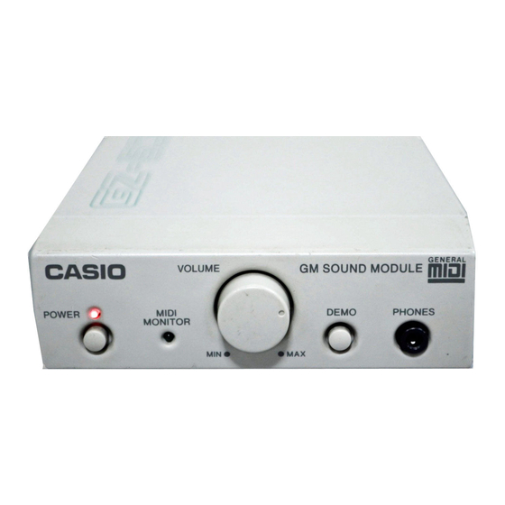
- Page 1 (with price) GZ-50M GENERAL GM SOUND MODULE VOLUME POWER MIDI DEMO PHONES MONITOR GM SOUND MODULE...
-
Page 2: Table Of Contents
Specifications ......... . 2 MIDI Messages receivable with GZ-50M ..... 3 Block Diagram . -
Page 3: Midi Messages Receivable With Gz-50M
MIDI messages receivable with GZ-50M MIDI channel: 1 - 16 channel Note On/Off: Note number 0 - 127 Velocity 1 - 127 Program change: 0 - 127 on channel 1 -9 & 11 - 16 0 - 7 on channel 10... - Page 4 The initial setteings Pitch bend: Modulation: 0 (Off) Expression: 127 (Maximum) Sustain: 0 (Off) Sostenuto: 0 (Off) Soft: 0 (Off) Channel pressure: 0 (Off) RPN: Null The initial settings in The General MIDI system Channel 1 - 9 & 11 - 16 Program change: 000 (Piano) Pitch bend:...
-
Page 5: Midi Implementation Chart
GZ-50M MIDI Implementation Chart Model Version: 1.0 Function ... Transmitted Recognized Remarks Basic Default 1-16 channel Channel Changed 1-16 channel Default Mode 3 Mode Messages Altered Note 0 ~ 127 Number: True voice *1:Different per tones. 12 ~ 108 Velocity... - Page 6 LIST OF TONES AND OCTAVE RANGES TONE NO./TONE NAME GM OCTAVE RANGE TONE NO./TONE NAME GM OCTAVE RANGE PIANO BASS 000 PIANO 032 WOOD BASS E1 – G3 A0 – C8 001 HARD PIANO 033 ELEC BASS 1 E1 – G3 A0 –...
- Page 7 TONE NO./TONE NAME GM OCTAVE RANGE TONE NO./TONE NAME GM OCTAVE RANGE REED SYNTH-SFX 064 SOPRANO SAX F#3 – D#6 096 PEARL DROP C2 – C7 065 ALTO SAX C#3 – G#5 097 SOUNDTRACK C2 – C7 066 TENOR SAX F#2 –...
- Page 8 LIST OF DRUM SOUNDS NOTE NO. DRUM INSTRUMENT NAME Acoustic Bass Drum Bass Drum 1 Side Stick Acoustic Snare Hand Clap Electric Snare Low Floor Tom Closed Hi Hat High Floor Tom Pedal Hi Hat Low Tom Open Hi Hat Low Mid Tom High Mid Tom Crash Cymbal 1...
-
Page 9: Block Diagram
BLOCK DIAGRAM MIDI IN Photocoupler Reset IC IC106 IC104 RESET PC900VP RH5VL36A LSI104 HD6433298A42F Power Switch POWER Power ON signal A0 ~ D0~D7 Working Storage RAM (64K-bit) LSI106 SRM2264LM90-B A0 ~ A14 A0 ~ A3 RA0 ~ RA19 Effect RAM Sound Source ROM EA0 ~ EA14 (256K-bit) -
Page 10: Circuit Description
CIRCUIT DESCRIPTION CPU (LSI104: HD6433298A42F) The 16-bit CPU contains a 32k-bit ROM, a 1k-bit RAM, seven 8-bit I/O ports and MIDI interfaces. The CPU receives MIDI message and interprets it using the working storage RAM. For instance, when receiv- ing NOTE ON message, the CPU sends the note number and its velocity to the DSP in order to produce sound of that note. - Page 11 Pin No. Terminal In/Out Function 1 ~ 8 CD0 ~ CD7 In/Out Data bus 9, 10 CE1, TRSB — Not used GND7 Ground (0V) source CK16 Terminal for 24.576 MHz clock check point VCC1 +5V source Clock input. Connected to terminal CK16. TCKB —...
- Page 12 Pin No. Terminal In/Out Function EOEB Read enable signal output for the effect RAM VCC7 +5V source ECEB Chip select signal output for the effect RAM 113 ~ 117 ED11 ~ ED15 — Not used VCC4 +5V source GND4 Ground (0V) source 120 ~ 122 ED8 ~ ED10 —...
- Page 13 Pin No. Terminal In/Out Function Mode selection terminal. Connected to ground. D.GND Ground (0V) source for the internal digital circuit Not used. DVDD +5V source for the internal digital circuit A.GND Ground (0V) source for the right channel R.OUT Right channel sound waveform output 7, 8 A.VDD +5V source for the internal analog circuit...
-
Page 14: Major Waveforms
MAJOR WAVEFORMS 0.1 s 0.1 s CH1: CH2: 5 V CH1: CH2: 5 V Voltage VDD Power ON trigger -NMI Emitter of Q105 HD6433298A42F pin 5 Initial reset signal Power ON signal RH5VL36A pin 1 HD6433298A42F pin 59 Reset signal HD6433298A42F pin 3 5 µs 2 ms... - Page 15 1 ms 1 ms CH1: 50 mV CH2: 50 mV CH1: 50 mV CH2: .5 V DAC output Line out amp. input (L-ch) UPD6376GS pin 11 C111 Filter output Line out amp. output (L-ch) M5218AFP pin 1 C161 1 ms Program change (Tone No) : 078 (Whistle) Note No.
-
Page 16: Pcb View And Check Points
PCB VIEW AND CHECK POINTS J101 J104 IC106 R181R182 Q110R176 C164 C162 R184 D109 X101 IC104 C137 R144 C138 R158 R159 LSI103 C157 LSI101 C125 C136 C117 C120 Q105 C135 C106 R109 C131 C118 C110 Q103 C104 R130 R134 D102 C119 C121 C109... -
Page 17: Schematic Diagram
SCHEMATIC DIAGRAM PCBs JCM304-MA1M/MA2M — 17 —... -
Page 18: Exploded View
EXPLODED VIEW — 18 —... -
Page 19: Parts List
PARTS LIST GZ-50M Notes: Prices and specifications are subject to change with- out prior notice. As for spare parts order and supply, refer to the "GUIDEBOOK for Spare parts Supply", published seperately. The numbers in item column correspond to the same... - Page 20 FOB Japan Item Code No. Parts Name Specification N.R.Yen Unit Price Main PCB M304-MA1M 6923 7150 PCB ass'y M304-MA1M with M140210*1 7,880 M304-MA2M LSI101 2114 4221 UPD6376GS-E1 LSI102 2012 0777 LC33832M-70-TLM LSI103 2012 1316 HG51B155FD-1 1,160 LSI104 2012 0462 HD6433298A42F LSI105 2012 1498 TC5316200CF-C117...
- Page 21 MA0700951A...