Table of Contents
Advertisement
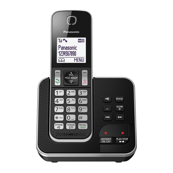
KX-TGDA30
(Handset)
(Charger Unit)
Configuration for each model
Model No
Base Unit
KX-TGD320 1 (TGD320) 1 (TGDA30)
KX-TGD322 1 (TGD320) 2 (TGDA30)
KX-TGD323 1 (TGD320) 3 (TGDA30)
KX-TGDA30
*KX-TGDA30 is also an optional accessory, which contains a handset
and a charger.
KX-TGD320
(Base Unit)
Handset
Charger Unit Expendable
1
2
1 (TGDA30)
1
Model No.
Digital Cordless Answering System
B: Black & Silver frame Version
(for Australia)
Up to 6
Up to 6
Up to 6
ORDER NO. KM41512971CE
Telephone Equipment
KX-TGD320ALB
KX-TGD322ALB
KX-TGD323ALB
KX-TGDA30AZB
© Panasonic System Networks Co., Ltd. 2016
Unauthorized copying and distribution is a violation
of law.
Advertisement
Table of Contents
Troubleshooting

Related Manuals for Panasonic KX-TGD320ALB


Summary of Contents for Panasonic KX-TGD320ALB
- Page 1 KX-TGD323 1 (TGD320) 3 (TGDA30) Up to 6 KX-TGDA30 1 (TGDA30) *KX-TGDA30 is also an optional accessory, which contains a handset and a charger. © Panasonic System Networks Co., Ltd. 2016 Unauthorized copying and distribution is a violation of law.
- Page 2 KX-TGD320ALB/KX-TGD322ALB/KX-TGD323ALB/KZ-TGDA30AZB WARNING This service information is designed for experienced repair technicians only and is not designed for use by the general public. It does not contain warnings or cautions to advise non-technical individuals of potential dangers in attempting to service a product. Products powered by electricity should be serviced or repaired only by experienced professional technicians.
-
Page 3: Table Of Contents
KX-TGD320ALB/KX-TGD322ALB/KX-TGD323ALB/KX-TGDA30AZB TABLE OF CONTENTS PAGE PAGE 1 Safety Precautions----------------------------------------------- 5 9.2.1. Check Point (Base Unit) --------------------------- 40 1.1. For Service Technicians --------------------------------- 5 9.3. Troubleshooting by Symptom (Handset)----------- 42 2 Warning -------------------------------------------------------------- 5 9.3.1. Check Point (Handset) ----------------------------- 42 2.1. Battery Caution--------------------------------------------- 5 10 Disassembly and Assembly Instructions--------------- 45 10.1. - Page 4 KX-TGD320ALB/KX-TGD322ALB/KX-TGD323ALB/KZ-TGDA30AZB 14.2.1. Component View ------------------------------------ 79 14.3. Handset (Main) ------------------------------------------- 81 14.3.1. Component View ------------------------------------ 81 14.3.2. Bottom View ------------------------------------------ 82 14.4. Handset (Module) ---------------------------------------- 83 14.4.1. Component View ------------------------------------ 83 14.4.2. Bottom View ------------------------------------------ 83 15 Exploded View and Replacement Parts List ----------- 84 15.1.
-
Page 5: Safety Precautions
KX-TGD320ALB/KX-TGD322ALB/KX-TGD323ALB/KX-TGDA30AZB 1 Safety Precautions 1.1. For Service Technicians • Repair service shall be provided in accordance with repair technology information such as service manual so as to prevent fires, injury or electric shock, which can be caused by improper repair work. -
Page 6: Suggested Pbf Solder
KX-TGD320ALB/KX-TGD322ALB/KX-TGD323ALB/KZ-TGDA30AZB 2.2.1. Suggested PbF Solder There are several types of PbF solder available commercially. While this product is manufactured using Tin, Silver, and Copper (Sn+Ag+Cu), you can also use Tin and Copper (Sn+Cu) or Tin, Zinc, and Bismuth (Sn+Zn+Bi). Please check the manufacturer’s specific instructions for the melting points of their products and any precautions for using their product with other materials. -
Page 7: Specifications
KX-TGD320ALB/KX-TGD322ALB/KX-TGD323ALB/KX-TGDA30AZB 3 Specifications L Standard: DECT (Digital Enhanced Cordless Telecommunications), GAP (Generic Access Profile) L Frequency range: 1.88 GHz to 1.90 GHz L RF transmission power: Approx. 10mW (average power per channel) L Power source: 220 - 240 V AC, 50/60 Hz... -
Page 8: Technical Descriptions
KX-TGD320ALB/KX-TGD322ALB/KX-TGD323ALB/KZ-TGDA30AZB 4 Technical Descriptions 4.1. Block Diagram (Base Unit_Main) -
Page 9: Block Diagram (Base Unit_Rf Part)
KX-TGD320ALB/KX-TGD322ALB/KX-TGD323ALB/KX-TGDA30AZB 4.2. Block Diagram (Base Unit_RF Part) ANT1... -
Page 10: Circuit Operation (Base Unit)
KX-TGD320ALB/KX-TGD322ALB/KX-TGD323ALB/KZ-TGDA30AZB 4.3. Circuit Operation (Base Unit) General Description: (BBIC, Flash Memory, EERROM) is a digital speech/signal processing system that implements all the functions of speech compression, record and playback, and memory management required in a digital telephone answering machine. The BBIC system is fully controlled by a host processor. The host processor provides activation and control of all that functions as follows. -
Page 11: Power Supply Circuit/Reset Circuit
KX-TGD320ALB/KX-TGD322ALB/KX-TGD323ALB/KX-TGDA30AZB 4.3.4. Power Supply Circuit/Reset Circuit The power supply voltage from AC adaptor is converted to VBAT (3.0V) in IC302. And +3.0V for peripherals and analog part is insulated from VBAT by Doubler of BBIC. Circuit Operation: +3.0V VBAT IC601... - Page 12 KX-TGD320ALB/KX-TGD322ALB/KX-TGD323ALB/KZ-TGDA30AZB 4.3.4.1. Charge Circuit The voltage from the AC adaptor is supplied to the charge circuits. +5.5V F301 CHARGE+ CHARGE-...
-
Page 13: Telephone Line Interface
KX-TGD320ALB/KX-TGD322ALB/KX-TGD323ALB/KX-TGDA30AZB 4.3.5. Telephone Line Interface Telephone Line Interface Circuit: Function • Bell signal detection • ON/OFF hook and pulse dial circuit • Side tone circuit Bell signal detection and OFF HOOK circuit: In the idle mode, Q141 is open to cut the DC loop current and decrease the ring load. When ring voltage appears at the Tip (T) and Ring (R) leads (When the telephone rings), the AC ring voltage is transferred as follows: T ... -
Page 14: Transmitter/Receiver
KX-TGD320ALB/KX-TGD322ALB/KX-TGD323ALB/KZ-TGDA30AZB 4.3.6. Transmitter/Receiver • Audio Circuits and DTMF tone signal circuits. Base Unit and Handset mainly consist of RF Module and DECT BBIC. Base Unit and Handset transmit/receive voice signal and data signal through the antenna on carrier frequency. Signal Path: *Refer to Signal Route(P.18). -
Page 15: Block Diagram (Handset)
KX-TGD320ALB/KX-TGD322ALB/KX-TGD323ALB/KX-TGDA30AZB 4.4. Block Diagram (Handset) -
Page 16: Circuit Operation (Handset)
KX-TGD320ALB/KX-TGD322ALB/KX-TGD323ALB/KZ-TGDA30AZB 4.5. Circuit Operation (Handset) 4.5.1. Outline Handset consists of the following ICs as shown in Block Diagram (Handset) (P.15). • DECT BBIC (Base Band IC): IC1 - All data signals (forming/analyzing ACK or CMD signal) - All interfaces (ex: Key, Detector Circuit, Charge, DC/DC Converter, EEPROM, LCD, RF Power Amp.) -
Page 17: Behavior Of Electric Power Failure
KX-TGD320ALB/KX-TGD322ALB/KX-TGD323ALB/KX-TGDA30AZB 4.6. Behavior of Electric Power Failure When AC power is lost and lose radio waves, Module PCB turns Q11 on and, battery voltage appear to CHG terminal. When CHG+ (supply voltage from handset) is higher than Vbat, Q351 is on. And, this unit continues working in power failure condition. -
Page 18: Signal Route
KX-TGD320ALB/KX-TGD322ALB/KX-TGD323ALB/KZ-TGDA30AZB 4.7. Signal Route ROUTE SIGNAL ROUTE MIC (+) - C13 - RA4 - IC1 (17) IC1(86) C859 - ANT to BASE HANDSET TX MIC (–) - C11 - RA4 - IC1 (18) IC1(87) ---ANT. - <BASE_UNIT_RF_RX_ROUTE> - IC501(46/47 - 28) - L101 - C184 - Q161 - Q141... - Page 19 KX-TGD320ALB/KX-TGD322ALB/KX-TGD323ALB/KX-TGDA30AZB RF part signal route SIGNAL ROUTE ROUTE HANDSET RF IC1(86/87) - C859 - ANT [ TX_ROUTE ] HANDSET RF ANT - IC(1/2) [ RX_ROUTE ] IC501(44/45) - C819 - C872 - ANT BASE UNIT RF [ TX_ROUTE ] ANT - C872 - C895 - IC501(46/47)
-
Page 20: Location Of Controls And Components
KX-TGD320ALB/KX-TGD322ALB/KX-TGD323ALB/KZ-TGDA30AZB 5 Location of Controls and Components Refer to the Operating Instructions. Note: You can download and refer to the Operating Instructions (Instruction book) on TSN Server. 6 Installation Instructions Refer to the Operating Instructions. Note: You can download and refer to the Operating Instructions (Instruction book) on TSN Server. -
Page 21: Test Mode
KX-TGD320ALB/KX-TGD322ALB/KX-TGD323ALB/KX-TGDA30AZB 8 Test Mode 8.1. Engineering Mode 8.1.1. Base Unit Important: Make sure the address on LCD is correct when entering new data. Otherwise, you may ruin the unit. } (Power) Soft keys Navigator key/ (Volume) key/ (Phonebook)/ (Caller list) key/... - Page 22 KX-TGD320ALB/KX-TGD322ALB/KX-TGD323ALB/KZ-TGDA30AZB Frequently Used Items (Base Unit) ex.) Items Address Default Data New Data Remarks C-ID (FSK) sensitivity 09 16/09 17 28/00 1C/00 14/00 When hex changes from “00/28” to “00/1C” or (3 dB up) (6 dB up) “00/14”, gain increases by 3 dB or 6 dB.
-
Page 23: Handset
KX-TGD320ALB/KX-TGD322ALB/KX-TGD323ALB/KX-TGDA30AZB 8.1.2. Handset Important: Make sure the address on LCD is correct when entering new data. Otherwise, you may ruin the unit. } (Power) { Soft keys Navigator key/ (Volume) key/ (Phonebook)/ (Caller list) key/ (Talk) (Redial) key/ RECALL {... - Page 24 KX-TGD320ALB/KX-TGD322ALB/KX-TGD323ALB/KZ-TGDA30AZB Frequently Used Items (Handset) ex.) Items Address Default Data New Data Possible Adjusted Possible Adjusted Remarks Value MAX (hex) Value MIN (hex) Sending Level 07 76 Adjusted value Given value (*2) Receiving Level 07 77 Adjusted value Given value...
-
Page 25: Ves Area Layout In Flash (Handset)
KX-TGD320ALB/KX-TGD322ALB/KX-TGD323ALB/KX-TGDA30AZB 8.2. VES area layout in Flash (Handset) 8.2.1. Scope The purpose of this section is to describe the layout of the VES (Virtual EEPROM Storage) area in FLASH (IC4) for the Handset. The VES area contains hardware, software, and user specific parameters. Some parameters are set during production of the handset, some are set by the user when configuring the handset, and some during normal use of the phone. -
Page 26: How To Clear User Setting
KX-TGD320ALB/KX-TGD322ALB/KX-TGD323ALB/KZ-TGDA30AZB 8.3. How to Clear User Setting Units are reset to the Factory settings by this operation (Erase recorded Voice messages, stored Phone numbers, Caller list and etc.) Note: • Some menus are not reset. Refer to Operating Instructions (P.20). -
Page 27: Troubleshooting Guide
KX-TGD320ALB/KX-TGD322ALB/KX-TGD323ALB/KX-TGDA30AZB 9 Troubleshooting Guide 9.1. Troubleshooting Flowchart FLOW CHART Not working Power ON Base Unit Check Power Not playback Playback Pre-Message Check Playback Not record Record Check Record Link No link No charge Battery Charge Check Battery Charge Check Link... -
Page 28: Check Power
KX-TGD320ALB/KX-TGD322ALB/KX-TGD323ALB/KZ-TGDA30AZB 9.1.1. Check Power 9.1.1.1. Base Unit Is the AC Adaptor inserted into AC outlet? (*1) AC Adaptor. Is output voltage of AC adaptor 5.5 V? Check (*2) Check Power Supply Circuit. Check VDDC (1.2 V): Test Point [VDDC] (*2) RSTN: Reset = "High"? -
Page 29: Check Record
KX-TGD320ALB/KX-TGD322ALB/KX-TGD323ALB/KX-TGDA30AZB 9.1.2. Check Record 9.1.2.1. Base Unit A) Not record Incoming Message Check Telephone Line Interface Check Bell signal. [Bell]. Check Telephone Line Interface Does the unit catch line? [OFF HOOK]. Check Line In: Pin 16 of BBIC. Check ICM Recording in Signal Route. -
Page 30: Check Battery Charge
KX-TGD320ALB/KX-TGD322ALB/KX-TGD323ALB/KZ-TGDA30AZB 9.1.4. Check Battery Charge 9.1.4.1. Base Unit Plug in the AC Power source. Charge Handset on Base Unit. Check Charge Circuit of Base Unit. Is the voltage of two charge contacts about 5.5 V or more? Check Handset. Check Charge Contacts at... -
Page 31: Check Link
KX-TGD320ALB/KX-TGD322ALB/KX-TGD323ALB/KX-TGDA30AZB 9.1.5. Check Link 9.1.5.1. Base Unit Does Base Unit make link with normal working Base Unit is OK. Check Handset. Handset? (*1) Is the voltage of VBAT about 3.0 V? Check around Power Supply Circuit. (*1) Is the voltage of VDDC about 1.2 V? (*1) Is the voltage of +3.0V about 3.0 V? - Page 32 KX-TGD320ALB/KX-TGD322ALB/KX-TGD323ALB/KZ-TGDA30AZB 9.1.5.2. Handset Does Handset make link with Base Unit? Handset is OK. Check Base Unit. (Correct working unit) (*1) Is the voltage of "1.8V" about 1.8 V? Adjust 1.8V voltage to 1.8 V. Check around Power Supply Circuit/Reset Circuit .
-
Page 33: Check The Rf Part
KX-TGD320ALB/KX-TGD322ALB/KX-TGD323ALB/KX-TGDA30AZB 9.1.6. Check the RF part 9.1.6.1. Finding out the Defective part 1. Prepare Regular HS(*1) and Regular BU(*2). 2. a. Re-register regular HS (Normal mode) to base unit (to be checked). If this operation fails in some ways, the base unit is defective. - Page 34 KX-TGD320ALB/KX-TGD322ALB/KX-TGD323ALB/KZ-TGDA30AZB 9.1.6.2. RF Check Flowchart Each item (1 ~ 6) of RF Check Flowchart corresponds to Check Table for RF part (P.35). Please refer to the each item. Start Link Control Check BBIC interface parts. confirmation signal (RF Block <->BBIC on BU/HS P.C.B)
- Page 35 KX-TGD320ALB/KX-TGD322ALB/KX-TGD323ALB/KX-TGDA30AZB 9.1.6.3. Check Table for RF part Item BU (Base Unit) Check HS (Handset) Check Link Confirmation Normal 1. Register Regular HS to BU (to be 1. Register HS (to be checked) to Regular checked). HS, BU Mode [Normal Mode] 2.
- Page 36 KX-TGD320ALB/KX-TGD322ALB/KX-TGD323ALB/KZ-TGDA30AZB 9.1.6.4. TEST RANGE Check Circuit block which range is defective can be found by the following check. Item BU (Base Unit) Check HS (Handset) Check Range Confirmation TX TEST 1. Register Regular HS to BU (to be checked). 1. Register HS (to be checked) to Regular BU.
-
Page 37: Registering A Handset To The Base Unit
KX-TGD320ALB/KX-TGD322ALB/KX-TGD323ALB/KX-TGDA30AZB 9.1.7. Registering a Handset to the Base Unit 1 Handset: # 1 3 0 { } : Select a base unit number. i {OK} L This number is used by the handset as a reference only. 3 Base unit: Press and hold { } for about 5 seconds. -
Page 38: Check Handset Transmission
KX-TGD320ALB/KX-TGD322ALB/KX-TGD323ALB/KZ-TGDA30AZB 9.1.9. Check Handset Transmission Check MIC of handset. Check handset Tx in Signal Route. Cross Reference: Signal Route (P.18) 9.1.10. Check Handset Reception Check speaker of handset. Check handset Rx in Signal Route. Cross Reference: Signal Route (P.18) Note: When checking the RF part, Refer to Check the RF part (P.33). -
Page 39: Check Bell Reception
KX-TGD320ALB/KX-TGD322ALB/KX-TGD323ALB/KX-TGDA30AZB 9.1.12. Check Bell Reception 9.1.12.1. Base Unit When bell signal is coming, is there bell sound Check around C101, C102, C110, C112, C113, R113, signal at BBIC (IC501 5pin : BELL)? R114, R111, R112, P101, D113, Q111 Check IC501 of Base Unit. -
Page 40: Troubleshooting By Symptom (Base Unit)
KX-TGD320ALB/KX-TGD322ALB/KX-TGD323ALB/KZ-TGDA30AZB 9.2. Troubleshooting by Symptom (Base Unit) If your unit has below symptoms, follow the instructions in remedy column. Remedies depend on whether you have DECT tester (*1) or not. Remedy (*2) Symptom You have DECT Tester. You don’t have DECT Tester. - Page 41 KX-TGD320ALB/KX-TGD322ALB/KX-TGD323ALB/KX-TGDA30AZB Items Check Procedure Check or Point Replace Parts (H)* Transmitted Power ANT1 Short ANT1 pattern to GND. IC501, C810 Confirmation 1. Configure the DECT tester (CMD60) as follows; C811, C819 <Setting> C820, C863 • Test mode: FP C871, C872 •...
-
Page 42: Troubleshooting By Symptom (Handset)
KX-TGD320ALB/KX-TGD322ALB/KX-TGD323ALB/KZ-TGDA30AZB 9.3. Troubleshooting by Symptom (Handset) If your unit has below symptoms, follow the instructions in remedy column. Remedies depend on whether you have DECT tester (*1) or not. Symptom Remedy (*2) You don’t have DECT Tester. You have DECT Tester. - Page 43 KX-TGD320ALB/KX-TGD322ALB/KX-TGD323ALB/KX-TGDA30AZB Items Check Procedure Check or Point Replace Parts (F)* Battery Monitor Check 1. Apply 2.25 V between BATT+ and BATT-. IC1, R45 2. Execute the command sendchar PAD sendchar LED 0 sendchar CRX 0 1 sendchar AD1 It assumes that the return value is XX.
- Page 44 KX-TGD320ALB/KX-TGD322ALB/KX-TGD323ALB/KZ-TGDA30AZB Items Check Procedure Check or Point Replace Parts (O) SP phone Audio Check 1. Link to Base which is connected to Line Simulator. IC1, C78, C79, and Confirmation 2. Set line voltage to 48 V and line current to 50 mA.
-
Page 45: Disassembly And Assembly Instructions
KX-TGD320ALB/KX-TGD322ALB/KX-TGD323ALB/KX-TGDA30AZB 10 Disassembly and Assembly Instructions 10.1. Disassembly Instructions 10.1.1. Base Unit Remove the 4 screws to remove the cabinet cover. Remove the solders. Solders... - Page 46 KX-TGD320ALB/KX-TGD322ALB/KX-TGD323ALB/KZ-TGDA30AZB Remove screw to remove Screw the jack holder and the charge case. Jack Holder Flip the Main P. C. Board and Solder unsolder to remove the Main P. C. Board Main P. C. Board Remove 3 screws. Remove the Operational P. C. Board Screw Operational P.
-
Page 47: Handset
KX-TGD320ALB/KX-TGD322ALB/KX-TGD323ALB/KX-TGDA30AZB 10.1.2. Handset 2 screws Remove the 2 screws. Insert a plastic card. Cabinet body (Ex. Used SIM card etc.) between the cabinet body and the cabinet cover, then pull it along the gap to open the cabinet. Cabinet cover Likewise, open the other side of the cabinet. -
Page 48: Charger Unit
KX-TGD320ALB/KX-TGD322ALB/KX-TGD323ALB/KZ-TGDA30AZB 10.1.3. Charger Unit Solders Charge Terminals... -
Page 49: How To Replace The Handset Lcd
KX-TGD320ALB/KX-TGD322ALB/KX-TGD323ALB/KX-TGDA30AZB 10.2. How to Replace the Handset LCD Note: The illustrations are simplified in this page. They may differ from the actual product. P. C. board Vertical Interval Tolerance Peel off the FFC (Flexible Flat Cable) from 0.2 mm the LCD, in the direction of the arrow. Take care to ensure that the foil on the P.C. -
Page 50: Measurements And Adjustments
KX-TGD320ALB/KX-TGD322ALB/KX-TGD323ALB/KZ-TGDA30AZB 11 Measurements and Adjustments This chapter explains the measuring equipment, the JIG connection, and the PC setting method necessary for the measurement in Troubleshooting Guide (P.27) 11.1. Equipment Required • Digital multi-meter (DMM): it must be able to measure voltage and current. -
Page 51: Connections (Base Unit)
KX-TGD320ALB/KX-TGD322ALB/KX-TGD323ALB/KX-TGDA30AZB Note: *: If you have the JIG Cable for TCD500 series (PQZZ1CD505E), change the following values of resistance. Then you can use it as a JIG Cable for both TCD300 and TCD500 series. (It is an upper compatible JIG Cable.) Resistor Old value (k) -
Page 52: How To Install Batch File Into P.c
KX-TGD320ALB/KX-TGD322ALB/KX-TGD323ALB/KZ-TGDA30AZB 11.2.2. How to install Batch file into P.C. Insert the Batch file CD-ROM into CD-ROM drive and copy PNZZTG**** folder to your PC (example: D drive). <Example for Windows> On your computer, click [Start], select Programs Open an MS-DOS mode window. -
Page 53: Adjustment Standard (Base Unit)
KX-TGD320ALB/KX-TGD322ALB/KX-TGD323ALB/KX-TGDA30AZB 11.3. Adjustment Standard (Base Unit) When connecting the simulator equipment for checking, please refer to below. 11.3.1. Bottom View VBAT (A) ANT1 Short R104 C 1 6 7 R124 R148 Q144 DECT Tester CHG- CTS60 (H)(I)(J)(K)(L) C113 Q111 CHG+... -
Page 54: The Setting Method Of Jig (Handset)
KX-TGD320ALB/KX-TGD322ALB/KX-TGD323ALB/KZ-TGDA30AZB 11.4. The Setting Method of JIG (Handset) This section explains the PC setting to use command required in Check Point (Handset)(P.42). <Preparation> • Serial JIG cable: PQZZ1CD300E* • PC which runs in DOS mode • Batch file CD-ROM for setting: Refer to parts list of Fixtures and Tools (P.91). -
Page 55: How To Install Batch File Into P.c
KX-TGD320ALB/KX-TGD322ALB/KX-TGD323ALB/KX-TGDA30AZB 11.4.2. How to install Batch file into P.C. Insert the Batch file CD-ROM into CD-ROM drive and copy PNZZTG***** folder to your PC (example: D drive). <Example for Windows> Open an MS-DOS mode window. On your computer, click [Start], select Programs... -
Page 56: Adjustment Standard (Handset)
KX-TGD320ALB/KX-TGD322ALB/KX-TGD323ALB/KZ-TGDA30AZB 11.5. Adjustment Standard (Handset) When connecting the simulator equipment for checking, please refer to below. 11.5.1. Component View P N L B 2 4 3 2 Z * K X - T G D A 3 0 x x... -
Page 57: Things To Do After Replacing Ic Or X'tal
KX-TGD320ALB/KX-TGD322ALB/KX-TGD323ALB/KX-TGDA30AZB 11.6. Things to Do after Replacing IC or X'tal If repairing or replacing EEPROM and X'tal, it is necessary to download the required data such as Programming data or adjustment data, etc. in memory. The set doesn't operate if it is not executed. - Page 58 KX-TGD320ALB/KX-TGD322ALB/KX-TGD323ALB/KZ-TGDA30AZB 11.6.1.2. Handset First, operate the PC setting according to The Setting Method of JIG (P.50). Then download the appropriate data according to the following procedures. Items How to download/Required adjustment FLASH(IC4) Adjusted parameter data is 1) Please be sure to execute the following steps if you have replaced the FLASH stored in memory.
- Page 59 KX-TGD320ALB/KX-TGD322ALB/KX-TGD323ALB/KX-TGDA30AZB 11.6.1.2.1. How to update the BBIC. • Execute COM communicator.exe 1. Initialize COM port.(Only once at first.) Select “Setting” “Serial port” “Initial settings” “OK”. Setting Serial Port Setting Cancel 2.Select serial port COM number. Select “Setting” “Serial port” “Setting” “OK”.
- Page 60 KX-TGD320ALB/KX-TGD322ALB/KX-TGD323ALB/KZ-TGDA30AZB • Execute COM communicator.exe again <<Write program>> 1. Select “Addon” “ProgramLoader”. 2. Select "Setting" "Config". Fill up the “ConfigSettings”. Note: (2) Select Baud Rate as 57600. If write error happens, select slower Baud Rate (example: 19200). 3. Select download file.
- Page 61 KX-TGD320ALB/KX-TGD322ALB/KX-TGD323ALB/KX-TGDA30AZB 4. Start download. (1). Connect Unit and 3wire jig. (2). Confirm "Turn on power to target and press download." display. (3). Power off the unit, then power on. (4). Press "Download" button again. 5. Finish download. Completed dialog means "Download finished successfully!." It takes more than 20 minutes to download ( It depends on baud rate).
-
Page 62: Rf Specification
KX-TGD320ALB/KX-TGD322ALB/KX-TGD323ALB/KZ-TGDA30AZB 11.7. RF Specification 11.7.1. Base Unit Item Value Refer to -. * TX Power 18.5 dBm ~ 25 dBm Check Point (Base Unit) (H) Modulation -350 ± 50/+350 ± 50 kHz/div Check Point (Base Unit) (I) Frequency Offset <±20 kHz... -
Page 63: Miscellaneous
KX-TGD320ALB/KX-TGD322ALB/KX-TGD323ALB/KX-TGDA30AZB 12 Miscellaneous 12.1. How to Replace the Flat Package IC Even if you do not have the special tools (for example, a spot heater) to remove the Flat IC, with some solder (large amount), a soldering iron and a cutter knife, you can easily remove the ICs that have more than 100 pins. -
Page 64: How To Install The Ic
KX-TGD320ALB/KX-TGD322ALB/KX-TGD323ALB/KZ-TGDA30AZB 12.1.3. How to Install the IC 1. Temporarily fix the FLAT PACKAGE IC, soldering the two marked pins. *Check the accuracy of the IC setting with the corresponding soldering foil. 2. Apply flux to all pins of the FLAT PACKAGE IC. -
Page 65: How To Replace The Shield Case
KX-TGD320ALB/KX-TGD322ALB/KX-TGD323ALB/KX-TGDA30AZB 12.2. How to Replace the Shield Case 12.2.1. Preparation • PbF (: Pb free) Solder • Soldering Iron Tip Temperature of 700 F ± 20 F (370 C ± 10 C) Note: We recommend a 30 to 40 Watt soldering iron. An expert may be able to use a 60 to 80 Watt iron where someone with less experience could overheat and damage the PCB foil. -
Page 66: How To Install The Shield Case
KX-TGD320ALB/KX-TGD322ALB/KX-TGD323ALB/KZ-TGDA30AZB 12.2.4. How to Install the Shield Case Note: • If you don’t have special tools (ex. Hot air disordering tool), conduct the following operations. • Shield case’s No. : PNMC1091Z 1. Put the shield case. 2. Solder the surroundings. -
Page 67: Terminal Guide Of The Ics, Transistors And Diodes
KX-TGD320ALB/KX-TGD322ALB/KX-TGD323ALB/KX-TGDA30AZB 12.3. Terminal Guide of the ICs, Transistors and Diodes 12.3.1. Base Unit Cathode (Reverse View) Anode 2SC6054JSL, B1ABDM000001 B1ABCE000009, DRC9113Z0L C0DBEYY00102 DA2J10100L C2HBCY000157 B1ADNB000003 Cathode Anode Cathode Anode B0ECKM000008 B0BC02000015 DSC7003S0L B1ACGP000008 B0EDER000009 Cathode Anode PNWIBD320ALH B3AAB0000347 PNWIAGD320GH 12.3.2. Handset... -
Page 68: Schematic Diagram
KX-TGD320ALB/KX-TGD322ALB/KX-TGD323ALB/KZ-TGDA30AZB 13 Schematic Diagram 13.1. For Schematic Diagram 13.1.1. Base Unit (Base Unit (Main)) Notes: 1. DC voltage measurements are taken with voltmeter from the negative voltage line. Important Safety Notice: Components identified by mark have special characteristics important for safety. - Page 69 KX-TGD320ALB/KX-TGD322ALB/KX-TGD323ALB/KX-TGDA30AZB Memo...
-
Page 70: Base Unit (Main)
KX-TGD320ALB/KX-TGD322ALB/KX-TGD323ALB/KZ-TGDA30AZB 13.2. Base Unit (Main) RF Block ANT1 ANT- Pattern +3.0V Wm=0.4mm ANt1_Short Lm=10mm C872 1.3p C895 C873 C871 ANT1_S-GND 1.1p SHORT1 SHORT R172 680k C175 W 0.2mm W 0.15mm 560p L 3.8mm L 6.2mm Q171 1st layer 1st layer W=0.3mm... - Page 71 KX-TGD320ALB/KX-TGD322ALB/KX-TGD323ALB/KX-TGDA30AZB *Q141 *R160 C101 680p R141 100k D101 Q161 *Q140 *R149 C102 680p *Q144 *R154 P101 L101 DC Monitor R115 5.6M NL_CID R116 5.6M Caller ID REFERENCE 1XX : TEL LINE R121 390k C121 680p 3XX : POWER, CHARGE R122...
-
Page 72: Handset (Main)
KX-TGD320ALB/KX-TGD322ALB/KX-TGD323ALB/KZ-TGDA30AZB 13.3. Handset (Main) 13.3.1. Main P. C. Board To Battery C101 VBAT VBAT Charge Current 2.5A ANT pattern BATT+ BATT+_ ANT-Short K0.1u [for Korea] ANT tuning pattern BATT-_ SOCp BATT- ANT-Short-GND ANT1_TP J39p SOCn SHORT2 *Q10 *R10 *Q11 *R13... - Page 73 KX-TGD320ALB/KX-TGD322ALB/KX-TGD323ALB/KX-TGDA30AZB Memo...
-
Page 74: Module P. C. Board
KX-TGD320ALB/KX-TGD322ALB/KX-TGD323ALB/KZ-TGDA30AZB 13.3.2. Module P. C. Board GND_1 VBAT BELL_LED1 BELL_LED1 BATTERY_ON Battery_ON STB_B STB_B STB_E STB_E VBAT STB_A STB_A KEY_LED KEY_LED MICh MICh MIC- MIC- GND_2 SOCp GND_3 SOCp REC+ REC+ SOCn REC- REC- SOCn CHG+ CHG+ BAT-/SOCp SOCp SOCn... - Page 75 KX-TGD320ALB/KX-TGD322ALB/KX-TGD323ALB/KX-TGDA30AZB *open-stub SLx2 RF BLOCK W1=0.2mm L1=3.3mm RX-balun W2=0.7mm L2=5.0mm W=0.170mm 50 ohm line W=0.25mm L=3.6mm L=2mm L=2mm S=0.125mm RF_RXn RX_RF C863 W=0.25mm 1.8p L=2mm 50 ohm line SHORT RF_RXp Total L=4mm +1.8V W=0.3mm W=0.3mm W=0.25mm C859 L=6.95mm L=6.5mm L=5mm...
- Page 76 KX-TGD320ALB/KX-TGD322ALB/KX-TGD323ALB/KZ-TGDA30AZB Memo...
-
Page 77: Printed Circuit Board
KX-TGD320ALB/KX-TGD322ALB/KX-TGD323ALB/KX-TGDA30AZB 14 Printed Circuit Board 14.1. Base Unit (Main) 14.1.1. Component View Q141 P101 KX-TGD320 MAIN BOARD (Base Unit (Component View)) -
Page 78: Bottom View
KX-TGD320ALB/KX-TGD322ALB/KX-TGD323ALB/KZ-TGDA30AZB 14.1.2. Bottom View R104 C 1 6 7 R124 R148 Q144 C113 Q111 C120 R373 R114 RSTN RSTN RSTN C515 R 9 2 4 +3.0V +3.0V STM/CKM/P1 STM/CKM/P15 R371 VDDC VDDC IC601 F301 C 3 2 1 IC611 R 3 2 1... -
Page 79: Base Unit (Operation)
KX-TGD320ALB/KX-TGD322ALB/KX-TGD323ALB/KX-TGDA30AZB 14.2. Base Unit (Operation) 14.2.1. Component View LOCATOR ERASE DOWN SKIP REPEAT P b F T G D 3 2 x H P N L B 2 4 2 9 Z A - R C LED901 LED902 R E F - 1... - Page 80 KX-TGD320ALB/KX-TGD322ALB/KX-TGD323ALB/KZ-TGDA30AZB Memo...
-
Page 81: Handset (Main)
KX-TGD320ALB/KX-TGD322ALB/KX-TGD323ALB/KX-TGDA30AZB 14.3. Handset (Main) 14.3.1. Component View P N L B 2 4 3 2 Z * K X - T G D A 3 0 x x P b F CP4V R E F - 2 CP3V 1.8V CKM (10.368MHz) -
Page 82: Bottom View
KX-TGD320ALB/KX-TGD322ALB/KX-TGD323ALB/KZ-TGDA30AZB 14.3.2. Bottom View P N L B 2 4 3 2 Z * K X - T G D A 3 0 x x P b F R E F - 2 KX-TGDA30 MAIN BOARD (Handset (Bottom View)) -
Page 83: Handset (Module)
KX-TGD320ALB/KX-TGD322ALB/KX-TGD323ALB/KX-TGDA30AZB 14.4. Handset (Module) 14.4.1. Component View CP4V JTAG C190 C862 P N L B 2 4 3 1 Z * T G D A / T G K A 3 x R 0 KX-TGDA30 MODULE BOARD (Handset (Component View)) 14.4.2. -
Page 84: Exploded View And Replacement Parts List
KX-TGD320ALB/KX-TGD322ALB/KX-TGD323ALB/KZ-TGDA30AZB 15 Exploded View and Replacement Parts List 15.1. Cabinet and Electrical Parts (Base Unit) (*1) (*2) CUSHION/LCD (No. 105) PCB2 (*2) PCB1 (*1) Ref.No. Figure 2.6 x 8mm Note: (*1)(*2) This SPACERs are cut from the excess parts of CUSHION/LCD (No.105). -
Page 85: Cabinet And Electrical Parts (Handset)
(*1) This cable is fixed by welding. Refer to How to Replace the Handset LCD (P.49). (*2) The rechargeable Ni-MH Panasonic Battery is available through sales route of Panasonic. (*3) Attach the SPACER (No. 114) to the exact location described above. -
Page 86: Cabinet And Electrical Parts (Charger Unit)
KX-TGD320ALB/KX-TGD322ALB/KX-TGD323ALB/KZ-TGDA30AZB 15.3. Cabinet and Electrical Parts (Charger Unit) 200-1 200-3 200-2 200-4 200-5... -
Page 87: Accessories
KX-TGD320ALB/KX-TGD322ALB/KX-TGD323ALB/KX-TGDA30AZB 15.4. Accessories... -
Page 88: Replacement Parts List
KX-TGD320ALB/KX-TGD322ALB/KX-TGD323ALB/KZ-TGDA30AZB 15.5. Replacement Parts List Safety Ref. Part No. Part Name & Description Remarks 1. RTL (Retention Time Limited) PQJJ1T039M JACK, MODULAR Note: PNKF1369Z1 CABINET COVER PS-HB The “RTL” marking indicates that its Retention Time is PNHA1013Z RUBBER PARTS, FOOT CUSHION Limited. -
Page 89: Handset
KX-TGD320ALB/KX-TGD322ALB/KX-TGD323ALB/KX-TGDA30AZB Safety Ref. Part No. Part Name & Descripti Remarks Safety Ref. Part No. Part Name & Descripti Remarks R142 PQ4R18XJ272 2.7k C508 ECUE1H100DCQ 10p R145 ERJ2GEJ222 2.2k C509 ECUE1H120JCQ 12p R148 ERJ2GEJ103 C510 ECUE0J105KBQ 1 R149 D0GA681JA021 680 C511... - Page 90 KX-TGD320ALB/KX-TGD322ALB/KX-TGD323ALB/KZ-TGDA30AZB 15.5.2.2. Main P.C.Board Parts Safety Ref. Part No. Part Name & Description Remarks Note: ECUE1H222KBQ 0.0022 (*1) Reconfirm the model No. written on the handset’s name ECUV1C105KBV 1 plate when replacing PCB100. Because the model No. of ECUE0J105KBQ 1 the optional handset may differ from the included handset.
-
Page 91: Charger Unit
KX-TGD320ALB/KX-TGD322ALB/KX-TGD323ALB/KX-TGDA30AZB 15.5.3. Charger Unit 15.5.3.1. Cabinet and Electrical Parts Safety Ref. Part No. Part Name & Description Remarks PNLC1064ZB CHARGER UNIT ASS'Y without NAME PLATE (RTL) 200-1 PNKM1609Z1 CABINET BODY PS-HB 200-2 PNJT1182Z CHARGE TERMINAL 200-3 PNJJ021001Z JACK, MODULAR 200-4...