Table of Contents
Advertisement
Quick Links
Advertisement
Table of Contents

Related Manuals for Motorola EVB555


Summary of Contents for Motorola EVB555
- Page 1 MPC555 Evaluation Board Quick Reference...
- Page 3 Motorola reserves the right to make changes without further notice to any products herein. Motorola makes no warranty, representation or guarantee regarding the suitability of its products for any particular purpose, nor does Motorola assume any liability arising out of the application or use of any product or circuit, and specifically disclaims any and all liability, including without limitation consequential or incidental damages.
-
Page 5: Table Of Contents
TABLE OF CONTENTS Preface 9 Technical Features of the EVB555 11 Overview of the Evaluation Board 13 Interfaces and Configuration Possibilities 15 Power Supply 15 Supply Voltage Connection 15 Standby 15 Power On 15 Single Chip/External Bus Mode 15 Single Chip Mode 15... - Page 6 CO 104/105—Customized Communication Expansion (CAN) 50 CO 106/107—Host Communication Expansion 50 CO 500-505—Logic Analyzer Ports: Digital Signals 50 CO 506/507—Logic Analyzer Ports: Analog Signals 51 CO 508—ETK Connector 51 CO 509—Lauterbach Connector 51 CO 600-603—MAPI Interface 51 CO 604—PRU Extension 51 MOTOROLA EVB555 Quick Reference...
-
Page 7: Preface
SECTION 1 Preface The EVB555 is an MPC555-based evaluation board that can be used for the develop- ment and test of microcontroller systems. The MPC555 is a member of the Motorola MPC500 PowerPC™ Risc microcontroller family. Beside its PowerPC core and the internal memory subsystem it has a number of peripheral components (eg. - Page 8 MOTOROLA EVB555 1-10 Quick Reference...
-
Page 9: Technical Features Of The Evb555
SECTION 2 Technical Features of the EVB555 The following list summarizes the technical features of the EVB555 evaluation board. The architecture of the board is displayed in Figure 2-1 on the following page. • General advantages — Full function range of the MPC555 can be used —... - Page 10 Figure 2-1 Architecture of the EVB555 evaluation board...
-
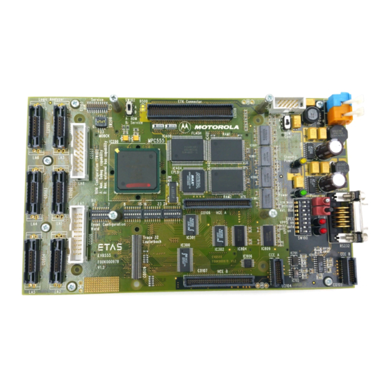
Page 11: Overview Of The Evaluation Board
SECTION 3 Overview of the Evaluation Board Figure 3-1 EVB555 Top EVB555 MOTOROLA Quick Reference 3-13... - Page 12 Figure 3-2 EVB555 Bottom MOTOROLA EVB555 3-14 Quick Reference...
-
Page 13: Interfaces And Configuration Possibilities
The toggle switch Power On (SW703) is used for activating the operating voltage of the EVB555. The activated state is shown by the additional LED Power On (LD702, green). All modules on the evaluation board are now supplied with power. -
Page 14: External Bus Interface
4.2.2 External Bus Interface The external bus makes it possible to use the resources of the EVB555, such as SRAM, Flash-EEPROM or host communication expansion. The pins are used here for addresses and data. Section 5.2. explains how the general purpose I/O lines are still available on the EVB555. -
Page 15: Programming The Flash Modules
1. The pin can be permanently connected to a high level with the ”EPEE” (SW100-4 on) switch 2. The ETK can enable the programming mode by a high level at the SGEPEE signal (C0508, pin 137). EVB555 MOTOROLA Quick Reference 4-17... -
Page 16: Interfaces For Testing And Debugging
The MAPI-400+100 interface makes it possible to expand the EVB555 with extensive and customer-specific hardware. For example, there could be signal converters and output drivers connected to extend the EVB555 to a test sample of a control unit for industrial use. -
Page 17: Reset And Reset Configuration
The reset configuration is read by the MPC555 after the supply voltage is switched on and after a hard reset has occurred. Setting the hard reset configuration is conveniently solved on the EVB555 by assign- ing the hard reset configuration word via 32 DIP switches. - Page 18 1: internal flash enabled 0: little endian swap logic inactive CLES 1: little endian swap logic active 28:30 Initial internal space base (6.12.1.2) 0: dual mapping disabled 1: dual mapping enabled Table 4-1 Hard reset configuration word MOTOROLA EVB555 4-20 Quick Reference...
-
Page 19: Configuration Of The Pll
Please consult the MPC555 User Manual for an explanation of the PLL function and limp mode. The standard setting for the evaluation board should be ”010”. The PLL works using the quartz crystal assembled on the EVB555 (4 MHz) whereby the limp mode is enabled. EVB555... - Page 20 MOTOROLA EVB555 4-22 Quick Reference...
-
Page 21: Working With The Evb555
SECTION 5 Working with the EVB555 5.1 Using External Resources The external resources on the board (RAM, Flash-EEPROM, PRU) can be addressed through the external bus interface. The selection takes place via chip select signals. Figure 5-1 shows the connection of the external devices to the most important bus control signals of the MPC555. - Page 22 The memory size assigned to chip select 1 (/CS1) of the MPC555 should therefore be 4 Mbyte. If the units intended for the higher addresses are not used, this area can also be selected to be smaller (e.g. only 2 Mbyte for RAM and PRU). MOTOROLA EVB555 5-24 Quick Reference...
-
Page 23: Working With The Pru
A7A8 xx00 external RAM xx01 0000 0000 PRU_CONF 0000 0100 PRU_DATA1 0000 1000 PRU_DATA2 0001 0000 EPLD Version 0001 1100 Vpp12 Control xx10 ETK Piggyback Host xx11 Communication Extension Figure 5-3 Address decoding by EPLD EVB555 MOTOROLA Quick Reference 5-25... -
Page 24: Notes On The External Flash Memory
To be able to start a program without a BDM debugger, it is necessary to boot from non-volatile memory (i.e., from flash memory). The mode can be set via the reset con- figuration word (see Section 4.6.2.). There are a few points about the EVB555 that should be observed. -
Page 25: Connector Assignment
APPENDIX A Connector Assignment The following tables display the connector assignment of the EVB555 evaluation board. Only the connected pins are listed; all other pins are open. EVB555 MOTOROLA Quick Reference A-27... -
Page 26: Mapi-400+100 Interface
Interrupt request, SGPIO, address type: indicates one of the 16 ”address types”. The address type signals are /IRQ4B_SGP valid at the rising edge of the clock in which the special transfer start (STS) is asserted. MOTOROLA EVB555 A-28 Quick Reference... - Page 27 IRQ5B, no SGPIO Interrupt request, mode clock [2]: /IRQ6B_mck2 similar to IRQ5B, no SGPIO Flash supply voltage (5V) used during program and erase operation of the CMF. 28, 41, 46, 71, Ground 74, 89, EVB555 MOTOROLA Quick Reference A-29...
-
Page 28: Assignment Of J2/P2 (Co601) Connector
Receive data: serial input from the SCI1 TXD1_QGPO Transmit data: serial output from the SCI1 RXD2_QGPI Receive data: serial input from the SCI2 TXD2_QGPO Transmit data: serial output from the SCI2 MDA30 See MDA11 MDA31 See MDA11 MPIO5 GPIO MPIO6 GPIO MOTOROLA EVB555 A-30 Quick Reference... - Page 29 GPIO MPIO14 GPIO MPIO15 GPIO BAN0_PQB0 See AAN0_PQB0 BAN1_PQB1 See AAN0_PQB0 BAN2_PQB2 See AAN0_PQB0 BAN3_PQB3 See AAN0_PQB0 BAN48_PQB4 See AAN48_PQB4 BAN49_PQB5 See AAN48_PQB4 BAN50_PQB6 See AAN48_PQB4 17, 18, 43, 46, Ground 63, 64, 83, 84 EVB555 MOTOROLA Quick Reference A-31...
-
Page 30: Assignment Of J3/P3 (Co602) Connector
Visible history buffer flush status: to allow program instruction flow VFLS0_MPIO3 tracking. VFLS1_MPIO4 See VFLS0_MPIO3 Instruction watchpoint. Visible history buffer flush status: output by the IWP0_VFLS chip to enable program instruction flow tracking. IWP1_VFLS See IWP0_VFLS MOTOROLA EVB555 A-32 Quick Reference... - Page 31 Timer expired (output): status of the TEXPS bit in the PLPRCR register in the USIU. SGPIO freeze: RCPU is in debug mode FRZ_/PTR program trace (/PTR): an instruction fetch is taking place. 25, 43, 65, 68, Ground 81, 91, 95, 97 EVB555 MOTOROLA Quick Reference A-33...
-
Page 32: Assignment Of J4/P4 (Co603) Connector
Data_SGP0 is the MSB. Data_SGP0 Data_SGP3 Data_SGP2 Data_SGP5 Data_SGP4 Data_SGP7 Data_SGP6 Data_SGP9 Data_SGP8 Data_SGP11 Data_SGP10 Data_SGP13 Data_SGP12 Data_SGP15 Data_SGP14 Data_SGP17 Data_SGP16 Data_SGP19 Data_SGP18 Data_SGP21 Data_SGP20 Data_SGP23 Data_SGP22 Data_SGP25 Data_SGP24 Data_SGP27 Data_SGP26 Data_SGP29 Data_SGP28 Data_SGP31 Data_SGP30 MOTOROLA EVB555 A-34 Quick Reference... - Page 33 Output enable /CS2B Chip select /CS3B Chip select CLKOUT Clock out: can be configured to full strength, half strength or disabled. 15, 16, 27, 28, 39, 40, 57, 58, Ground 75, 76, 83, 93, 96 ,97 EVB555 MOTOROLA Quick Reference A-35...
-
Page 34: Pru Connector (Co604) Assignment
See A_PIO0 B_PIO12 See B_PIO0 A_PIO12 See A_PIO0 B_PIO13 See B_PIO0 A_PIO13 See A_PIO0 B_PIO14 See B_PIO0 A_PIO14 See A_PIO0 B_PIO15 See B_PIO0 A_PIO15 See A_PIO0 B_PIO16 See B_PIO0 A_PIO16 See A_PIO0 B_PIO17 See B_PIO0 MOTOROLA EVB555 A-36 Quick Reference... - Page 35 STANDBY switch EVB into Stanby mode 95, 96, 97, 98, alternative power supply path 99, 100 15, 16, 27, 28, 39, 40, 57, 58, 75, 76, Ground 83, 89, 90, 91, 92, 93, EVB555 MOTOROLA Quick Reference A-37...
-
Page 36: Assignment Of Logic Analyzer Interface
/CS[0] /CS0B ADDR /CS[1] /CS1B ADDR /CS[2] /CS2B ADDR /CS[3] /CS3B ADDR A[8] Addr_SGP8 ADDR A[9] Addr_SGP9 ADDR A[10] Addr_SGP10 ADDR A[11] Addr_SGP11 ADDR A[12] Addr_SGP12 ADDR A[13] Addr_SGP13 ADDR A[14] Addr_SGP14 ADDR A[15] Addr_SGP15 MOTOROLA EVB555 A-38 Quick Reference... -
Page 37: Assignment Of Co501 Connector
D[4] Data_SGP4 DATA D[5] Data_SGP5 DATA D[6] Data_SGP6 DATA D[7] Data_SGP7 DATA D[8] Data_SGP8 DATA D[9] Data_SGP9 DATA D[10] Data_SGP10 DATA D[11] Data_SGP11 DATA D[12] Data_SGP12 DATA D[13] Data_SGP13 DATA D[14] Data_SGP14 DATA D[15] Data_SGP15 EVB555 MOTOROLA Quick Reference A-39... -
Page 38: Assignment Of Co502 Connector
/BBB_IWP3 LWP[0] SGP_/IRQOUTB LWP[1] /BGB_LWP1 STAT DSCK TCK_DSCK STAT DSDO TDO_DSDO STAT DSDI TDI_DSDI STAT Compression pin STAT VF[0] VF0_MPIO0 STAT VF[1] VF1_MPIO1 STAT VF[2] VF2_MPIO2 1) designated to be used in future by HP MOTOROLA EVB555 A-40 Quick Reference... -
Page 39: Assignment Of Co503 Connector
MDA[13] (DA9) MDA31 MPWM[14] (PWM0) MPWM0 MPWM[15] (PWM1) MPWM1 MPWM[16] (PWM2) MPWM2 MPWM[17] (PWM3) MPWM3 MPWM[18] (PWM4) MPWM16 MPWM[19] (PWM5) MPWM17 MPWM[20] (PWM6) MPWM18 MPWM[21] (PWM7) MPWM19 Test point 501 Test point 502 Test point 503 EVB555 MOTOROLA Quick Reference A-41... -
Page 40: Assignment Of Co504 Connector
TPUCH[4] TPU_A A_TPUCH4 TPUCH[5] TPU_A A_TPUCH5 TPUCH[6] TPU_A A_TPUCH6 TPUCH[7] TPU_A A_TPUCH7 TPUCH[8] TPU_A A_TPUCH8 TPUCH[9] TPU_A A_TPUCH9 TPUCH[10] TPU_A A_TPUCH10 TPUCH[11] TPU_A A_TPUCH11 TPUCH[12] TPU_A A_TPUCH12 TPUCH[13] TPU_A A_TPUCH13 TPUCH[14] TPU_A A_TPUCH14 TPUCH[15] TPU_A A_TPUCH15 MOTOROLA EVB555 A-42 Quick Reference... -
Page 41: Assignment Of Co505 Connector
TPUCH[13] TPU_B B_TPUCH13 TPUCH[14] TPU_B B_TPUCH14 TPUCH[15] TPU_B B_TPUCH15 n.c. CNTX0_A A_CNTX0 CNRX0_A A_CNRX0 CNTX0_B B_CNTX0 CNRX0_B B_CNRX0 EPEE EPEE /IRQ[0]_SGPIOC[0] /IRQ0B_SGP /IRQ[5]_SGPIOC[5]_ /IRQ5B_SGP MODCK[1] /IRQ[6]_MODCK[2] /IRQ6B_mck2 /IRQ[7]_MODCK[3] /IRQ7B_mck3 /TRST /TRSTB n.c. n.c. n.c. n.c. n.c. EVB555 MOTOROLA Quick Reference A-43... -
Page 42: Assignment Of Co506 Connector
AAN48_PQB4 QADC_A AN[49]_PQB[5] AAN49_PQB5 QADC_A AN[50]_PQB[6] AAN50_PQB6 QADC_A AN[51]_PQB[7] AAN51_PQB7 QADC_A AN[52]_MA[0]_PQA[0] AAN52_PQA0 QADC_A AN[53]_MA[1]_PQA[1] AAN53_PQA1 QADC_A AN[54]_MA[2]_PQA[2] AAN54_PQA2 QADC_A AN[55]_PQA[3] AAN55_PQA3 QADC_A AN[56]_PQA[4] AAN56_PQA4 QADC_A AN[57]_PQA[5] AAN57_PQA5 QADC_A AN[58]_PQA[6] AAN58_PQA6 QADC_A AN[59]_PQA[7] AAN59_PQA7 QADC_A MOTOROLA EVB555 A-44 Quick Reference... -
Page 43: Assignment Of Co507 Connector
BAN48_PQB4 QADC_B AN[49]_PQB[5] BAN49_PQB5 QADC_B AN[50]_PQB[6] BAN50_PQB6 QADC_B AN[51]_PQB[7] BAN51_PQB7 QADC_B AN[52]_MA[0]_PQA[0] BAN52_PQA0 QADC_B AN[53]_MA[1]_PQA[1] BAN53_PQA1 QADC_B AN[54]_MA[2]_PQA[2] BAN54_PQA2 QADC_B AN[55]_PQA[3] BAN55_PQA3 QADC_B AN[56]_PQA[4] BAN56_PQA4 QADC_B AN[57]_PQA[5] BAN57_PQA5 QADC_B AN[58]_PQA[6] BAN58_PQA6 QADC_B AN[59]_PQA[7] BAN59_PQA7 QADC_B EVB555 MOTOROLA Quick Reference A-45... -
Page 44: Assignment Of Etk Connectors
SDATA[4] See SDATA[31] SGD28 SDATA[3] See SDATA[31] SGD29 SDATA[2] See SDATA[31] Ground SGD30 SDATA[1] See SDATA[31] SGD31 SDATA[0] See SDATA[31] SADDR7 - SADDR3: SGA0 SADDR[31] external address bus of MPC555 SGA1 SADDR[30] See SADDR[31] Ground MOTOROLA EVB555 A-46 Quick Reference... - Page 45 2: /SGINST /IRQ4_AT2 differentiate code or data access Ground /SGTS Transfer start: start of a bus cycle that transfers data /SGCSR /SGCSR Chip select for piggy-back on ETK Ground /SGTA Transfer acknowledge: transfer accepted/valid Ground EVB555 MOTOROLA Quick Reference A-47...
- Page 46 VFLS0_MPIO3 program instruction flow tracking. MPC input: will control the Flash-EEPROM SGEPEE SGEPEE program or erase operations. VF[0:2] visible instruction queue flush status: output by SGVF0 VF0_MPIO0 chip when program instruction flow tracking is required. MOTOROLA EVB555 A-48 Quick Reference...
- Page 47 Test point 519 SGPDIR3 (TP520) Test point 520 Ground SGCLKO EXTCLK External frequency source for the chip. /SGPWE (TP521) Test point 521 Ground Ground /SGF_SEL RESERVED 1) Resistor (0R0) to GND on the adapter (ETAP3) EVB555 MOTOROLA Quick Reference A-49...
-
Page 48: Connectors And Their Counterparts
Connectors and their Counterparts A.4.1 CO 100—Background Debug Mode Interface (BDM) CO 100 EVB555 Counterpart .100” x .100” Shrunk shrouds header, Description .100” x .100” Polarized socket, 10 pins 10 pins Manufacturer 8510-4500 JL (boardmount) Order No. 925320-01-10-10 CHG-2010-J01010-KCP (wiremount) A.4.2 CO 101—RS232 Serial Interface... -
Page 49: Co 506/507-Logic Analyzer Ports: Analog Signals
Micro Strips, 4 rows, 160 pins Please be sure to contact the manufacturer Manufacturer Samtec of your emulator probe for further informa- Order No. MOLC-140-02-S-Q-TR tion before connecting it to the EVB555. Comment A.4.9 CO 509—Lauterbach Connector CO 509 EVB555 Counterpart Description...