Sign In
Upload
Manuals
Brands
Motorola Manuals
Radio
XTL 1500
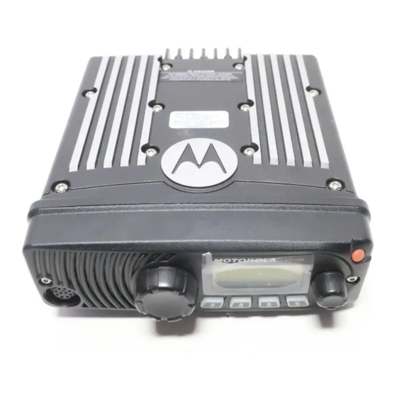
Motorola XTL 1500 Manuals
Manuals and User Guides for Motorola XTL 1500. We have
3
Motorola XTL 1500 manuals available for free PDF download: Detailed Service Manual, User Manual, Installation Manual
Motorola XTL 1500 Detailed Service Manual (452 pages)
Digtal, VHF/UHF Range 1/UHF Range 2/700–800 MHz
Brand:
Motorola
| Category:
Radio
| Size: 22.35 MB
Table of Contents
Motorola, Inc
2
Computer Software Copyrights
3
Foreword
3
Table of Contents
6
List of Figures
14
List of Tables
20
Related Publications
21
Commercial Warranty
22
Limited Warranty
22
Motorola Communication Products
22
General Provisions
22
What this Warranty Covers and for How Long
22
How to Get Warranty Service
23
State Law Rights
23
What this Warranty Does Not Cover
23
Governing Law
24
Patent and Software Provisions
24
Model Numbering, Charts, and Specifications
26
Mobile Radio Model Numbering Scheme
26
ASTRO XTL 1500 VHF 10-50 Watt Model Chart
27
ASTRO XTL 1500 UHF Range 1 10-40 Watt Model Chart
28
ASTRO XTL 1500 UHF Range 2 10-45 Watt Model Chart
29
ASTRO XTL 1500 700-800 Mhz 10-35 Watt Model Chart
30
VHF Radio Specifications
31
UHF Range 1 Radio Specifications
32
UHF Range 2 Radio Specifications
33
Mhz Radio Specifications
34
Chapter 1 Introduction
36
Notations Used in this Manual
36
General
36
Chapter 2 Product Overview
38
Introduction
38
Functional Blocks
38
Chapter 1 Introduction
38
Control-Head Assembly
39
Controller
39
Power Management (Power Control Microcontroller and Voltage Regulators)
39
Power Control Microcontroller
39
Voltage Regulators
39
User Interface (Keypad, STN Display, Volume and Frequency Knob) Section
39
Display
39
Backlight Leds
40
Keypad, Volume and Frequency Knob
40
Status Leds
40
Vehicle Interface Ports
41
Figure 2-1. VIP Dash-Mount Configuration
41
Receiver Section
42
VHF Band Radios
42
Back-End Section
42
Front-End Section
42
UHF Range 1/UHF Range 2 Band Radios
42
Intermediate Frequency and Back-End
42
Mhz Band Radios
43
Back-End Section
43
Front-End Section
43
Transmitter Section
43
VHF Radios
43
UHF Range 1/UHF Range 2 Radios
43
Mhz Radios
43
Circuit Protection
44
Output Network
44
Power Control
44
Rfpa
44
Frequency Generation Unit
44
VHF Mhz Radios
44
UHF Range 1/UHF Range 2 Radios
45
Mhz Radios
45
Controller Section
46
Analog Mode of Operation
46
Digital (ASTRO) Mode of Operation
47
Controller Section Circuitry
47
Chapter 3 Theory of Operation
50
Control Head Board
50
Control Head Board Major Sections
50
Controller Section
51
Power Management
52
Figure 3-3. Control Head Controller Block
52
Figure 3-4. Control Head Power Distribution
53
Power Distribution
53
Table 3-1. Integrated Circuits Voltages
54
Attiny13 Microcontroller Programming
55
Power up / Power down Sequence
55
Reset Circuits
55
Table 3-2. Attiny13 Programming Kit
55
User Interface
56
LCD Display
56
Keypad, Volume and Frequency Knob
56
GCAI Accessory Interface
56
Figure 3-5. GCAI Block Diagram
56
Main Board
57
Main Board Major Sections
57
VHF (136-174 Mhz) Band
57
Figure 3-6. XTL 1500 Main Board Sections (VHF MID Power)—Side 1
58
Figure 3-7. XTL 1500 Main Board Sections (VHF MID Power)—Side 2
59
UHF Range 1 (380-470 Mhz) and UHF Range 2 (450-520 Mhz) Band
60
Figure 3-9. XTL 1500 Main Board Sections (UHF Range 1 MID Power and UHF Range 2)—Side 2
61
Mhz Band
62
Figure 3-11. XTL 1500 Main Board Sections (700–800 Mhz)—Side 2
63
Radio Power Distribution
64
Figure 3-12. DC Voltage Routing Block Diagram (UHF Range 1 and UHF Range 2)
64
Receiver Front-End
65
VHF (136-174 Mhz) Band
65
Figure 3-13. DC Voltage Routing Block Diagram (VHF and 700-800 Mhz)
65
Db Step Attenuator (U3250)
66
Figure 3-14. Receiver Block Diagram (VHF)
66
Low-Noise Amplifiers (Q3255, Q3252)
66
PIN Diode Switches
66
Preselector Filters
66
Mixer (D3258)
67
UHF Range 1 (380-470 Mhz) Band
67
Figure 3-15. Receiver Front-End and Back-End (UHF Range 1)
67
Highpass Filter and First Low-Noise Amplifier
68
Image Filter
68
Low-Noise Amplifier (LNA, U5302)
68
Mixer
68
Preselector Filter
68
Switchable 15 Db Attenuator
68
UHF Range 2 (450-520 Mhz) Band
69
Figure 3-16. Receiver Front-End and Back-End (UHF Range 2)
69
Highpass Filter and First Low-Noise Amplifier
69
Image Filter
70
Low-Noise Amplifier (LNA, U5302)
70
Mixer
70
Preselector Filter
70
Switchable 15 Db Attenuator
70
Mhz Band
71
Figure 3-17. Receiver Front-End and Back-End (700-800 Mhz)
71
Low-Noise Amplifier (LNA, U6250)
71
Preselector Filters
71
Mixer (U6251)
72
Receiver Back-End
72
VHF (136-174 Mhz) Band
72
Abacus III IC
72
Intermediate Frequency (IF) Section
72
UHF Range 1 (380-470 Mhz) Band
73
Figure 3-18. ABACUS III (AD9874) IC Functional Block Diagram from Data Sheet (VHF)
73
Abacus III IC (U5002)
74
Figure 3-19. ABACUS III (AD9874) IC Functional Block Diagram from Data Sheet (UHF Range 1)
74
Intermediate Frequency (IF) Filter
74
UHF Range 2 (450-520 Mhz) Band
75
Abacus III IC (U5002)
75
Intermediate Frequency (IF) Filter
75
Mhz Band
76
Figure 3-20. ABACUS III (AD9874) IC Functional Block Diagram from Data Sheet (UHF Range 2)
76
Abacus III IC (U6000)
77
Figure 3-21. ABACUS III (AD9874) IC Functional Block Diagram from Data Sheet (700-800 Mhz)
77
Intermediate Frequency (IF) Filter
77
Transmitter
78
VHF (136-174 Mhz) Band
78
50-Watt Transmitter
78
Figure 3-22. 50-Watt RF Power Amplifier (RFPA) Gain Stages (VHF)
78
Figure 3-23. Output Network Components (VHF)
79
Output Network (ON)
79
Power Control
80
Figure 3-24. Power Control Components (VHF)
81
UHF Range 1 (380-470 Mhz) Band
82
40-Watt Transmitter
82
Figure 3-25. 40-Watt RF Power Amplifier (RFPA) Gain Stages (UHF Range 1)
82
Figure 3-26. Output Network Components (UHF Range 1)
83
Output Network (ON)
83
Power Control
84
Figure 3-27. Power Control Components (UHF Range 1)
85
UHF Range 2 (450-520 Mhz) Band
86
45-Watt Transmitter
86
Figure 3-28. 45-Watt RF Power Amplifier (RFPA) Gain Stages (UHF Range 2)
86
Figure 3-29. Output Network Components (UHF Range 2)
87
Figure 3-30. Power Control Components (UHF Range 2)
89
Mhz Band
90
35-Watt Transmitter
90
Figure 3-31. 35-Watt RF Power Amplifier (RFPA) Gain Stages (700-800 Mhz)
90
Figure 3-32. Output Network Components (700-800 Mhz)
91
Figure 3-33. Power Control Components (700-800 Mhz)
93
Frequency Generation Unit (FGU)
94
VHF (136-174 Mhz) Band
94
Reference Oscillator
95
LV Frac-N Synthesizer IC
95
Figure 3-34. Frequency Generation Unit Block Diagram (VHF)
95
Voltage Multiplier
96
Superfilter
96
Modulation
96
Figure 3-35. Waveform Representation During Programming of the LV Frac-N IC (VHF)
96
Charge Pump Bias
97
Loop Filter
97
Lock Detect
97
Transmitter Injection
97
Receiver Injection
98
Transmitter Vcos
98
Receiver Vcos
98
Prescaler Feedback
98
UHF Range 1 (380-470 Mhz) Band
98
Reference Oscillator
99
LV Frac-N Synthesizer IC
99
Figure 3-36. Frequency Generation Unit Block Diagram (UHF Range 1)
99
Voltage Multiplier
100
Superfilter
100
Modulation
100
Figure 3-37. Waveform Representation During Programming of the LV Frac-N IC (UHF Range 1)
100
Charge Pump Bias
101
Loop Filter
101
Lock Detect
101
Transmitter Injection
101
Receiver Injection
101
Transmitter Vcos
102
Receiver Vcos
102
Prescaler Feedback
102
Table 3-9. VCO aux Pin Logic UHF Range 1
102
UHF Range 2 (450-520 Mhz) Band
103
Figure 3-38. Frequency Generation Unit Block Diagram (UHF Range 2)
103
Figure 3-39. Waveform Representation During Programming of the LV Frac-N IC (UHF Range 2)
104
LV Frac-N Synthesizer IC
104
Reference Oscillator
104
Voltage Multiplier
104
Charge Pump Bias
105
Lock Detect
105
Loop Filter
105
Modulation
105
Superfilter
105
Receiver Injection
106
Receiver Vcos
106
Transmitter Injection
106
Transmitter Vcos
106
Prescaler Feedback
107
Mhz Band
107
Figure 3-40. Frequency Generation Unit Block Diagram (700-800 Mhz)
107
Figure 3-41. Waveform Representation During Programming of the LV Frac-N IC
108
LV Frac-N Synthesizer IC
108
Reference Oscillator
108
Voltage Multiplier
108
Charge Pump Bias
109
Lock Detect
109
Loop Filter
109
Modulation
109
Superfilter
109
Receiver Injection
110
Transmitter Injection
110
Transmitter Vcos
110
Controller Section
111
Figure 3-42. XTL 1500 Controller Section
112
Daughtercard Module
113
Figure 3-43. XTL 1500 Daughtercard Module
113
Controller DC Power Distribution
114
Figure 3-44. B+ Routing for Controller Section
114
Reset Circuits
115
Table 3-11. Integrated Circuits Voltages
115
Figure 3-45. Power-On Reset Circuit
116
Power-Up/Power-Down Sequence
116
Emergency Power-Up/-Down Sequence
117
MCU and DSP System Clocks
117
Power Turn-Off
117
Power Turn-On
117
Figure 3-46. Patriot IC (U100) UART Configuration
118
USB Bus
118
Serial Communications on the External Bus (SB9600)
119
Table 3-12. Rear Connector Naming Scheme
119
Figure 3-47. Serial Peripheral Interface (SPI) Block Diagram
120
Serial Peripheral Interface (SPI) Bus
120
Figure 3-48. XTL 1500 RX Signal Path
121
Receive Audio
121
Transmit Audio
122
Figure 3-49. XTL 1500 TX Signal Path
123
Figure 3-50. Boot RX and Boot TX Data Lines
124
Flash Programming
124
Reflashing/Upgrading Firmware
125
Table 3-14. Programming Cables
125
Receiver Vcos
111
Prescaler Feedback
111
Chapter 4 Troubleshooting Procedures
126
Introduction
126
Handling Precautions
126
Parts Replacement and Substitution
126
Rigid Circuit Boards
127
Heat-Related Precautions
127
Daughtercard Module
127
Sram
127
Testing
127
Voltage Measurement and Signal Tracing
128
Power-Up Self-Check Errors
128
Table 4-1. Power-Up Self-Check Error Codes
128
Operational Error Codes
130
Display Flashes "FAIL 001
130
Table 4-2. Operational Error Codes
130
VCO Hybrid Assembly
131
Table 4-3. Test Mode Channels
131
Table 4-4. VCO Frequency and Switching Logic
131
Out-Of-Lock Condition
132
FGU Troubleshooting Aids
132
Table 4-5. aux Output Frequency Requirements
132
Figure 4-1. Frequency Generator Unit DC Power Supply Distribution (VHF)
133
Figure 4-2. Frequency Generation Unit Block Diagram (VHF)
134
Table 4-6. LV Frac-N U3751 Pin Descriptions (VHF)
134
No or Low Output Power (TX or RX Injection)
136
No or Low Modulation
136
Troubleshooting the Back-End
136
UHF Range 1 (380-470 Mhz) Band Main Board Troubleshooting
136
Display Flashes "FAIL 001
136
Figure 4-3. Waveform Representation During Programming of the LV Frac-N IC (U3751)
136
Table 4-7. Test Mode Channels UHF Range 1 (aux 4 Is Not Used for VCO Selection in UHF)
137
Table 4-8. VCO Frequency Calculation and Switching Logic (UHF Range 1)
137
FGU Troubleshooting Aids
138
Figure 4-4. Frequency Generation Unit DC Power Supply Distribution (UHF Range 1)
138
Figure 4-5. Frequency Generation Unit Block Diagram (UHF Range 1)
139
Table 4-9. LV Frac-N U6751 Pin Descriptions (UHF Range 1)
139
No or Low Output Power (TX or RX Injection)
141
No or Low Modulation
141
Troubleshooting the Back-End
141
Figure 4-6. Waveform Representation During Programming of the LV Frac-N IC (U5752)
141
Out-Of-Lock Condition
141
Table 4-10. Test Mode Channels UHF Range 2 (aux 4 Is Not Used for VCO Selection in UHF)
142
Table 4-11. VCO Frequency Calculation and Switching Logic (UHF Range 2)
143
Figure 4-7. Frequency Generation Unit DC Power Supply Distribution (UHF Range 2)
144
Figure 4-8. Frequency Generation Unit Block Diagram (UHF Range 2)
145
Table 4-12. LV Frac-N U6751 Pin Descriptions (UHF Range 2)
145
Figure 4-9. Waveform Representation During Programming of the LV Frac-N IC (U5752)
147
Out-Of-Lock Condition
147
Table 4-13. Test Mode Channels (700-800 Mhz)
148
Table 4-14. VCO Frequency Calculation and Switching Logic (700-800 Mhz)
148
Figure 4-10. Frequency Generation Unit DC Power Supply Distribution (700-800 Mhz)
150
Figure 4-11. Frequency Generation Unit Block Diagram (700-800 Mhz)
151
Table 4-15. LV Frac-N U6751 Pin Descriptions (700-800 Mhz)
151
Standard Bias Tables
153
Figure 4-12. Waveform Representation During Programming of the LV Frac-N IC (U6751)
153
Table 4-16. Standard Operating Bias: Power Lines
153
Table 4-17. Standard Operating Bias: Clock and Control Lines
154
Table 4-18. Standard Operating Bias: Audio Lines
155
Receiver Front-End (RXFE)
157
VHF (136-174 Mhz) Band
157
UHF Range 1 (380-470 Mhz) Band
157
Table 4-19. Standard Operating Bias: VIP Lines (Dash Configuration)
157
UHF Range 2 (450-520 Mhz) Band
158
Mhz Band
158
Power Amplifier Procedures
158
VHF (136-174 Mhz) Band
158
50-Watt Power Amplifiers
158
General Troubleshooting and Repair Notes
158
UHF Range 1 (380-470 Mhz) Band
159
UHF Range 2 (450-520 Mhz) Band
159
Mhz Band
159
Chapter 5 Troubleshooting Charts
162
Introduction
162
List of Troubleshooting Charts
162
Figure 5-30. RF Power Amplifier (RFPA)-No or Low TX Power Output
162
Table 5-1. List of Troubleshooting Charts
162
Troubleshooting Tables
164
For VHF, UHF R1 and 700-800 Mhz Models
164
Table 5-2. XTL 1500 Troubleshooting Table (700-800 Mhz, 380-470 Mhz and 136-174 Mhz)
164
For UHF R2 Models
167
Table 5-4. XTL 1500 Receiver Troubleshooting Table (VHF Band)
170
Troubleshooting Test Points
171
Board ID Jumper Configuration
171
Figure 5-1. Main Board Test Points-Top Side
171
Figure 5-2. Main Board Test Points-Bottom Side
171
Flowcharts
172
Table 5-5. Board ID Jumper Configuration
172
Poor RX Sensitivity or no RX Audio (136-174 Mhz)-Part 1 of 2
173
Poor RX Sensitivity or no RX Audio (136-174 Mhz)-Part 2 of 2
174
Figure 5-5. RX IF-Poor SINAD or no Audio (136-174 Mhz)
175
RX IF-Poor SINAD or no Audio (136-174 Mhz)
175
RX Back-End-Poor SINAD or no Audio (136-174 Mhz)-Part 1 of 3
176
RX Back-End-Poor SINAD or no Audio (136-174 Mhz)-Part 2 of 3
177
RX Back-End-Poor SINAD or no Audio (136-174 Mhz)-Part 3 of 3
178
Figure 5-9. Low or no RX Injection Signal (136-174 Mhz)
179
Low or no RX Injection Signal (136-174 Mhz)
179
Figure 5-10. Low or no TX Injection Signal (136-174 Mhz)
180
Low or no TX Injection Signal (136-174 Mhz)
180
TX or RX VCO Unlock (Fail 001) (136-174 Mhz)-Part 1 of 2
181
TX or RX VCO Unlock (Fail 001) (136-174 Mhz)-Part 2 of 2
182
Figure 5-13. no Output Power at TX Mode (136-174 Mhz)
183
No Output Power at TX Mode (136-174 Mhz)
183
Figure 5-14. no Output Power and IDC < 2A at TX Mode (136-174 Mhz)
184
No Output Power and IDC < 2A at TX Mode (136-174 Mhz)
184
Figure 5-15. no 16.8 Mhz Reference Oscillator Frequency (380-470 Mhz and 450-520 Mhz)
185
No 16.8 Mhz Reference Oscillator Frequency (380-470 Mhz and 450-520 Mhz)
185
Poor RX Sensitivity or no RX Audio (380–470 Mhz and 450–520 Mhz)—Part 1 of 2
186
Poor RX Sensitivity or no RX Audio (380–470 Mhz and 450–520 Mhz)—Part 2 of 2
187
RX If—Poor SINAD or no Audio (380–470 Mhz and 450–520 Mhz)—Part 1 of 2
188
RX If—Poor SINAD or no Audio (380–470 Mhz and 450–520 Mhz)—Part 2 of 2
189
Part 1 of 3
190
RX Back-End—Poor SINAD or no Audio (380–470 Mhz and 450–520 Mhz Part 1 of 3
190
Figure 5-20. RX Back-End-Poor SINAD or no Audio (380-470 Mhz and 450-520 Mhz)
191
Figure 5-21. RX Back-End-Poor SINAD or no Audio (380-470 Mhz and 450-520 Mhz)
191
Figure 5-22. RX Back-End-Poor SINAD or no Audio (380-470 Mhz and 450-520 Mhz)
191
Part 2 of 3
191
Part 3 of 3
192
RX Back-End — Poor SINAD or no Audio (380–470 Mhz and 450–520 Mhz Part 3 of 3
192
Figure 5-23. Low or no RX Injection Signal (380-470 Mhz and 450-520 Mhz)
193
Low or no RX Injection Signal (380-470 Mhz and 450-520 Mhz)
193
Figure 5-24. Low or no TX Injection Signal (380-470 Mhz and 450-520 Mhz)
194
Low or no TX Injection Signal (380-470 Mhz and 450-520 Mhz)
194
Figure 5-25. no TX Audio (380-470 Mhz and 450-520 Mhz)
195
No TX Audio (380-470 Mhz and 450-520 Mhz)
195
TX or RX VCO Unlock (Fail 001) (380–470 Mhz and 450–520 Mhz)—Part 1 of 2
196
TX or RX VCO Unlock (Fail 001) (380–470 Mhz and 450–520 Mhz)—Part 2 of 2
197
Figure 5-28. RF Power Amplifier (RFPA)-No or Low TX Power Output
198
Mhz)-Part 1 of 5
198
Mhz)-Part 2 of 5
199
RF Power Amplifier (RFPA)-No or Low TX Power Output
199
Mhz)-Part 3 of 5
200
RF Power Amplifier (RFPA)-No or Low TX Power Output
200
Mhz)-Part 4 of 5
201
RF Power Amplifier (RFPA)-No or Low TX Power Output
201
Figure 5-29. RF Power Amplifier (RFPA)-No or Low TX Power Output
202
Mhz)-Part 5 of 5
202
Table 5-6. RFPA DC Voltages
202
Figure 5-31. RFPA Power Control-No VGBIAS (380-470 Mhz and 450-520 Mhz)
203
RFPA Power Control-No VGBIAS (380-470 Mhz and 450-520 Mhz)
203
Figure 5-32. no 16.8 Mhz Reference Oscillator Frequency (700-800 Mhz)
204
No 16.8 Mhz Reference Oscillator Frequency (700-800 Mhz)
204
Poor RX Sensitivity or no RX Audio (700-800 Mhz)-Part 1 of 2
205
Poor RX Sensitivity or no RX Audio (700-800 Mhz)-Part 2 of 2
206
Figure 5-35. RX IF-Poor SINAD or no Audio (700-800 Mhz)
207
RX IF-Poor SINAD or no Audio (700-800 Mhz)
207
RX Back-End-Poor SINAD or no Audio (700-800 Mhz)-Part 1 of 3
208
RX Back-End-Poor SINAD or no Audio (700-800 Mhz)-Part 2 of 3
209
RX Back-End-Poor SINAD or no Audio (700-800 Mhz)-Part 3 of 3
210
Figure 5-39. Low or no RX Injection Signal (700-800 Mhz)
211
Low or no RX Injection Signal (700-800 Mhz)
211
Figure 5-40. Low or no TX Injection Signal (700-800 Mhz)
212
Low or no TX Injection Signal (700-800 Mhz)
212
Figure 5-41. no TX Audio (700-800 Mhz)
213
No TX Audio (700-800 Mhz)
213
TX or RX VCO Unlock (Fail 001) (700-800 Mhz)-Part 1 of 2
214
TX or RX VCO Unlock (Fail 001) (700-800 Mhz)-Part 2 of 2
215
Figure 5-44. RF Power Amplifier (RFPA)-No or Low TX Power Output (700-800 Mhz)-Part 1 of 5
216
Part 1 of 5
216
Figure 5-45. RF Power Amplifier (RFPA)-No or Low TX Power Output (700-800 Mhz)-Part 2 of 5
217
Part 2 of 5
217
Figure 5-46. RF Power Amplifier (RFPA)-No or Low TX Power Output (700-800 Mhz)-Part 3 of 5
218
Part 3 of 5
218
Part 4 of 5
219
Part 5 of 5
220
Table 5-7. RFPA DC Voltages
220
Figure 5-47. RFPA Power Control-No K9.1V (700-800 Mhz)
221
RFPA Power Control-No K9.1V (700-800 Mhz)
221
Figure 5-48. RFPA Power Control-No VGBIAS (700-800 Mhz)
222
RFPA Power Control-No VGBIAS (700-800 Mhz)
222
RFPA Power Control-No or Low TX RFPA_CNTRL (700-800 Mhz)-Part 1 of 2
223
RFPA Power Control-No or Low TX RFPA_CNTRL (700-800 Mhz)-Part 2 of 2
224
Chapter 6 Troubleshooting Waveforms
226
Introduction
226
Table 6-1. List of Troubleshooting Waveforms
226
XTL 1500 Waveforms
227
Power-On Reset Timing
227
Power-On to Soft Turn-On Timing
227
Power-Down Reset
228
Mhz Clock Waveform
228
32 Khz Clock Waveform
229
DSP SSI Port RX Mode
229
DSP SSI Port TX Mode CSQ
230
SPI Bus Waveform
230
SB9600 Waveforms
231
SB9600 BUS+ and BUS- Waveforms
231
SB9600 BUS+ and RESET Waveforms
232
SB9600 BUSY and BUS- Waveforms
232
RX Waveforms
233
TX Waveforms
233
RX/TX Waveforms
234
USB Waveforms
234
Serial Audio Port Waveforms
235
Secure Interface Waveforms
235
Khz Frame Sync Waveform
236
RX Audio Waveforms
236
TX Audio Waveforms
237
TX and RX 1 Khz Audio Path Sinewave and Chart
237
Table 6-2. TX and RX Audio Path Test Points for 1 Khz Sine Wave
238
Table 6-3. TX and RX Audio Path Test Points for 1 Khz Sine Wave
239
Chapter 7 Schematics, Component Location Diagrams, and Parts Lists
240
List of Schematics, Component Location Diagrams, and Parts Lists
240
Table 7-1. List of Schematics, Component Location Diagrams, and Parts Lists
240
Control Head Main Board
242
Figure 7-1. Control Head Board Overall Block Diagram
242
Figure 7-2. Control Head Controller (OMAP Processor) Sheet 1 of 2
243
Figure 7-3. Control Head Controller (OMAP Processor) Sheet 2 of 2
244
Figure 7-4. Control Head Controller (SDRAM and Flash Memory)
245
Figure 7-5. TPS65012 Power Management IC, Factory Programming
246
Figure 7-6. Voltage Regulators
247
Figure 7-7. AVR Power Management Control
248
Figure 7-8. GCAI Accessory Interface (Sheet 1 of 2)
249
Figure 7-9. GCAI Accessory Interface (Sheet 2 of 2)
250
Figure 7-10. GCAI Connector Schematic
251
Figure 7-11. User Interface (Sheet 1 of 2)
252
Figure 7-12. User Interface (Sheet 2 of 2)
253
Figure 7-13. Rear Connector
254
Figure 7-14. Control Head Main Board Layout-Side 1 Top
255
Figure 7-15. Control Head Main Board Layout-Side 2 Bottom
256
Figure 7-16. GCAI Connector Board Layout-Side 1 Top
262
Figure 7-17. GCAI Connector Board Layout-Side 2 Bottom
263
HUD4022A (VHF) Main Board
265
Figure 7-18. HUD4022A Main Board Overall Block Diagram and Interconnections
265
Figure 7-21. HUD4022A Controller Urchin IC, MUX, and AD5320 DAC Schematic
268
Figure 7-22. HUD4022A Controller Audio Schematic
269
Figure 7-23. HUD4022A Controller Power Control (Sheet 1 of 2)
270
Figure 7-24. HUD4022A Controller Power Control (Sheet 2 of 2)
271
Figure 7-25. HUD4022A Frequency Generation Unit Overall Schematic (Sheet 1 of 2)
272
Figure 7-26. HUD4022A Frequency Generation Unit Overall Schematic (Sheet 2 of 2)
273
Figure 7-27. HUD4022A VHF Transmitter VCO Schematic
274
Figure 7-28. HUD4022A Frequency Generation Unit VHF Receive Injection Schematic
275
Figure 7-29. HUD4022A Frequency Generation Unit VHF Transmit Injection Schematic
276
Figure 7-30. HUD4022A Receiver Back-End Schematic
277
Figure 7-31. HUD4022A Receiver Front-End Schematic (Sheet 1 of 2)
278
Figure 7-32. HUD4022A Receiver Front-End Schematic (Sheet 2 of 2)
279
Figure 7-33. HUD4022A Receiver if Schematic
280
Figure 7-34. HUD4022A RF Power Amplifier (RF PA) Schematic (Sheet 1 of 2)
281
Figure 7-35. HUD4022A RF Power Amplifier (RF PA) Schematic (Sheet 2 of 2)
282
Figure 7-36. HUD4022A Secure Block Diagram and Interconnections
283
Figure 7-37. HUD4022A Accessory Connector Schematic
284
Figure 7-38. HUD4022A Power Supply Schematic
285
Figure 7-39. HUD4022A USB/RS232/SB9600 Schematic
286
Figure 7-40. HUD4022A SB9600 Schematic
287
Figure 7-41. HUD4022A USB/RS232/SB9600 VIP Input/Output Schematic
288
Figure 7-42. HUD4022A Control-Head Connector Schematic
289
Figure 7-43. HUD4022A Interface Connector Schematic
290
Figure 7-44. HUD4022A Main Board Layout-Side 1 Top
291
Figure 7-45. HUD4022A Main Board Layout-Side 1 Bottom
292
Figure 7-46. HUD4022A Main Board Layout-Side 2 Top
293
Figure 7-47. HUD4022A Main Board Layout-Side 2 Bottom
294
HUE4039A (UHF Range 1) Main Board
304
Figure 7-48. HUE4039A Main Board Overall Block Diagram and Interconnections
304
Figure 7-51. HUE4039A Controller Urchin IC, MUX, and AD5320 DAC Schematic
307
Figure 7-52. HUE4039A Controller Audio Schematic
308
Figure 7-53. HUE4039A Controller Power Control Schematic
309
Figure 7-54. HUE4039A Frequency Generation Unit
310
Figure 7-55. HUE4039A Receive VCO Schematic
311
Figure 7-56. HUE4039A Transmit VCO Schematic
312
Figure 7-57. HUE4039A Receiver Back-End Schematic
313
Figure 7-58. HUE4039A Receiver Front-End Schematic
314
Figure 7-59. HUE4039A Receiver Mixer Schematic
315
Figure 7-60. HUE4039A Receiver Preselector Schematic
316
Figure 7-61. HUE4039A Receiver if Schematic
317
Figure 7-62. HUE4039A RF Power Amplifier (RF PA) Schematic
318
Figure 7-63. HUE4039A Output Network (ON) Schematic
319
Figure 7-64. HUE4039A Secure Block Diagram and Interconnections
320
Figure 7-65. HUE4039A Rear Accessory Connector Schematic
321
Figure 7-66. HUE4039A Secure Power Supply Schematic
322
Figure 7-67. HUE4039A Secure USB/RS232/SB9600 Schematic
323
Figure 7-68. HUE4039A Secure SB9600 Schematic
324
Figure 7-69. HUE4039A Secure USB/RS232/SB9600 VIP Input/Output Schematic
325
Figure 7-70. HUE4039A Secure Control-Head Connector Schematic
326
Figure 7-71. HUE4039A Secure Interface Connector Schematic
327
Figure 7-72. HUE4039A Main Board Layout-Side 1 Top
328
Figure 7-73. HUE4039A Main Board Layout-Side 1 Middle
329
Figure 7-74. HUE4039A Main Board Layout-Side 1 Bottom
330
Figure 7-75. HUE4039A Main Board Layout-Side 2 Top
331
Figure 7-76. HUE4039A Main Board Layout-Side 2 Middle
332
Figure 7-77. HUE4039A Main Board Layout-Side 2 Bottom
333
HUE4040A (UHF Range 2) Main Board
345
Figure 7-78. HUE4040 Main Board Overall Block Diagram and Interconnections
345
Figure 7-79. HUE4040A Controller Block Diagram and Interconnections (Sheet 1 of 2)
346
Figure 7-80. HUE4040A Controller Block Diagram and Interconnections (Sheet 2 of 2)
347
Figure 7-81. HUE4040A Controller Urchin IC, MUX, and AD5320 DAC Schematic
348
Figure 7-82. HUE4040A Controller Audio Schematic
349
Figure 7-83. HUE4040A Controller Power Control Schematic
350
Figure 7-84. HUE4040A Frequency Generation Unit
351
Figure 7-85. HUE4040A Receive VCO Schematic
352
Figure 7-86. HUE4040A Transmit VCO Schematic
353
Figure 7-87. HUE4040A Receiver Back-End Schematic
354
Figure 7-88. HUE4040A Receiver Front-End Schematic
355
Figure 7-89. HUE4040A Receiver Mixer Schematic
356
Figure 7-90. HUE4040A Receiver Preselector Schematic
357
Figure 7-91. HUE4040A Receiver if Schematic
358
Figure 7-92. HUE4040A RF Power Amplifier (RF PA) Schematic
359
Figure 7-93. HUE4040A Output Network (ON) Schematic
360
Figure 7-94. HUE4040A Secure Block Diagram and Interconnections
361
Figure 7-95. HUE4040A Rear Accessory Connector Schematic
362
Figure 7-96. HUE4040A Secure Power Supply Schematic
363
Figure 7-97. HUE4040A Secure USB/RS232/SB9600 Schematic
364
Figure 7-98. HUE4040A Secure SB9600 Schematic
365
Figure 7-99. HUE4040A Secure Control-Head Connector Schematic (Sheet 1 of 2)
366
Figure 7-100.HUE4040A Secure Control-Head Connector Schematic (Sheet 2 of 2)
367
Figure 7-101.HUE4040A Secure Interface Connector Schematic
368
Figure 7-102.HUE4040A Main Board Layout-Side 1 Top
369
Figure 7-103.HUE4040A Main Board Layout-Side 1 Middle
370
Figure 7-104.HUE4040A Main Board Layout-Side 1 Bottom
371
Figure 7-105.HUE4040A Main Board Layout-Side 2 Top
372
Figure 7-106.HUE4040A Main Board Layout-Side 2 Middle
373
Figure 7-107.HUE4040A Main Board Layout-Side 2 Bottom
374
HUF4017A (700-800 Mhz) Main Board
386
Figure 7-108.HUF4017A Main Board Overall Block Diagram and Interconnections
386
Figure 7-109.HUF4017A Controller Block Diagram and Interconnections (Sheet 1 of 3)
387
Figure 7-110.HUF4017A Controller Block Diagram and Interconnections (Sheet 2 of 3)
388
Figure 7-111.HUF4017A Controller Block Diagram and Interconnections (Sheet 3 of 3)
389
Figure 7-112.HUF4017A Controller Audio Schematic
390
Figure 7-113.HUF4017A Power, Data, Secure, and Front/Rear Connector Block Diagrams
391
Figure 7-114.HUF4017A USB/RS232/SB9600 Schematic
392
Figure 7-115.Rear Accessory Connector (J0402) Schematic
393
Figure 7-116.Control-Head Front Connector Schematic
394
Figure 7-117.Controller Power Supply and Emergency Schematic
395
Figure 7-118.Controller RS232/SB9600 Schematic
396
Figure 7-119.Controller VIP Input/Output Schematic
397
Figure 7-120.Controller Secure Interface Connector Schematic
398
Figure 7-121.Secure Interface Board Schematic
399
Figure 7-122.HUF4017A Controller Urchin IC, MUX, and AD5320 DAC Schematic
400
Figure 7-123.HUF4017A Controller Power Supply Schematic
401
Figure 7-124.HUF4017A Receiver Back-End Schematic
402
Figure 7-125.HUF4017A Receiver Front-End Schematic (Sheet 1 of 2)
403
Figure 7-126.HUF4017A Receiver Front-End Schematic (Sheet 2 of 2)
404
Figure 7-127.HUF4017A Receiver Intermediate Frequency (IF) Schematic
405
Figure 7-128.HUF4017A RF Power Amplifier (PA) Schematic (Sheet 1 of 2)
406
Figure 7-129.HUF4017A RF Power Amplifier (PA) Schematic (Sheet 2 of 2)
407
Figure 7-130.HUF4017A Frequency Generation Unit Overall Schematic (Sheet 1 of 2)
408
Figure 7-131.HUF4017A Frequency Generation Unit Overall Schematic (Sheet 2 of 2)
409
Figure 7-132.HUF4017A Frequency Generation Unit 800 Mhz Receive Injection Schematic
410
Figure 7-133.HUF4017A Frequency Generation Unit 800 Mhz Transmit Injection Schematic
411
Figure 7-134.HUF4017A Main Board Layout-Side 1 Top
412
Figure 7-135.HUF4017A Main Board Layout-Side 1 Middle
413
Figure 7-136.HUF4017A Main Board Layout-Side 1 Bottom
414
Figure 7-137.HUF4017A Main Board Layout-Side 2 Top
415
Figure 7-138.HUF4017A Main Board Layout-Side 2 Middle
416
Figure 7-139.HUF4017A Main Board Layout-Side 2 Bottom
417
Figure 7-140.HUF4017A Daughtercard Module Board Layout
418
Chapter 8 Flex Cable Pin-Out Lists
428
List of Flex Cables
428
Flex Cables
428
Table 8-1. Dash Flex Cable J5000 to P0401 Pin-Out List
428
Table 8-2. Rear Accessory Flex Cable J2 to P0402 Pin-Out List
428
Appendix A Replacement Parts Ordering
430
Basic Ordering Information
430
Motorola Online
430
Mail Orders
430
Telephone Orders
430
Fax Orders
431
Parts Identification
431
Product Customer Service
431
A.5 Fax Orders
431
Glossary
432
Index
442
Advertisement
Motorola XTL 1500 User Manual (120 pages)
Digital Mobile Radio
Brand:
Motorola
| Category:
Radio
| Size: 5.41 MB
Table of Contents
Trunking Features
5
Alert Tones
7
Declaration of Conformity
9
Computer Software Copyrights
10
Documentation Copyrights
10
Disclaimer
10
Patent Disclosure
10
Notations Used in this Manual
11
Table of Contents
12
Getting to Know Your Radio
17
Major Radio Components
18
The XTL 1500 Radio
18
The Control Head
18
Using Your Radio: the Basics
20
Turning Your Radio on or off
20
Adjusting the Volume
21
Turning the Display/Keypad Light on or off
21
Entering Menus (Softkeys)
21
Returning to the HOME Display
22
Trunked Modes or Conventional Channels
22
Field Programming
22
Interpreting Radio Status Indicators
23
Entering Characters Using the Keypad
29
Basic Radio Operation
31
Monitoring Conventional Modes
32
Selecting a Zone and Mode (Channel)
33
Receiving on a Conventional Mode
34
Adjusting the Squelch Setting
34
Receiving on Trunked Systems
35
Transmitting on Conventional Modes
35
Transmitting on Trunked Systems
36
Time-Out Timer
37
Common Radio Features
39
Sending a Status Call (Trunking Only)
40
Selecting Transmit Power Level
42
Conventional Squelch Options
43
Analog Squelch Options
43
Digital Squelch Options
43
Sending an Emergency Alarm
44
Sending an Emergency Call
45
Special Considerations for Emergencies
46
Types of Scan
47
Turning Scan on or off
48
Deleting Nuisance Modes
48
PTT-ID (Optional)
49
Time-Out Timer
49
Telephone Operation (Conventional and Trunking)
50
Answering a Telephone Call
50
Call Alert (Conventional and Trunking)
51
Paging the Last ID Number Transmitted or Received
51
Entering Directly the ID Number to be Paged
51
Scrolling to an ID Number in the Page List
52
Going Directly to an ID Number in the Page List
53
Sending a Call Alert Page
54
Answering a Call Alert Page
55
Optional External Alarms (Horn And/Or Lights)
57
Turning External Alarm(S) on or off
57
When a Call Is Received While Alarms Are Turned on
58
Conventional Features
59
Repeater/Direct Operation
59
Status Calls (Digital Modes Only)
60
Sending a Status Call
60
Smart PTT
61
Talkgroup Calls
62
Selecting a Talkgroup
62
Selective Calls
63
Calling the Last ID Number Transmitted or Received
63
Entering Directly the ID Number to be Called
64
Scrolling to an ID Number in the Call List
65
Going Directly to an ID Number in the Call List
66
Starting a Selective Call
67
Trunking Features
69
Features Used on Trunking Systems
69
Viewing Your Radio's ID Number
70
Programming a Page or Call Number
71
Programming a Page or Call Name
74
Hang up Box (HUB)
76
Enhanced Private Conversation
76
Calling the Last ID Number Transmitted or Received
76
Entering Directly the ID Number to be Called
77
Scrolling to an ID Number in the Call List
78
Going Directly to an ID Number in the Call List
79
Sending a Private Conversation Call
80
Answering an Enhanced Private Conversation Call
81
Dynamic Regrouping
83
Electronic (Menu) Mode Selection
83
Selecting Enable and Disable
83
Smartzone Operation
84
Locking/Unlocking a Site
84
Searching for a Site
85
Site Trunking
86
Failsoft
86
Out-Of-Range Indication
87
Trunked Announcement
88
Initiating an Announcement
88
Secure Features
89
Features Available on Secure XTL 1500
89
Transmitting in Secure and Clear Modes
90
System Considerations
91
Loss Indication
91
Selecting a Key (Conventional Only)
92
Troubleshooting
93
Accessories
95
Antennas
95
Cables
96
Microphones
96
Miscellaneous
96
Speakers
96
Trunnion Kits
96
Appendix: Maritime Radio Use in the VHF Frequency Range
97
Special Channel Assignments
97
Emergency Channel
97
Non-Commercial Call Channel
98
Operating Frequency Requirements
98
Glossary
101
Commercial Warranty and Service
105
Limited Warranty
105
Service
109
Index
111
Control Head Foldout Page
117
Motorola XTL 1500 Installation Manual (60 pages)
Motorola Astro XTL 1500 Digital Mobile Radio Installation manual
Brand:
Motorola
| Category:
Radio
| Size: 4.24 MB
Table of Contents
Foreword
2
Parts Ordering
2
Computer Software Copyrights
2
Document Copyrights
2
Disclaimer
2
Trademarks
2
Installation Requirements for Compliance with Radio Frequency (RF) Energy Exposure Safety Standards
3
Table of Contents
5
Mobile Radio Model Numbering Scheme
10
Commercial Warranty
11
Limited Warranty
11
Motorola Communication Products
11
What this Warranty Covers and for How Long
11
General Provisions
11
State Law Rights
12
How to Get Warranty Service
12
What this Warranty Does Not Cover
12
Patent and Software Provisions
13
Governing Law
13
Chapter 1 Introduction
15
Mobile Radio Description
15
Dimensions
15
Figure 1-1. Front View of Dash Mount Brick Trunnion
15
Figure 1-2. Side View of Dash Mount Brick Trunnion
15
Dash Mount Configuration
16
Base/Control Stations
16
Figure 1-3. Dash Mount Configuration
16
Tools Required for XTL 1500 Installations
17
Chapter 2 Standard Configurations
19
Planning the Installation
19
Figure 2-1. Mounting Flexibility in Middle Console
20
Figure 2-2. on Top or under Dash Mounting
20
Figure 2-3. in Dash Mounting
20
Figure 2-4. Radio Installation with Transceiver
21
Wiring Diagrams
21
Radio Mounting
22
Figure 2-5. Trunnion Orientation
22
Figure 2-6. Transmission Hump Trunnion Mounting
23
Figure 2-7. below Dash Trunnion Mounting
23
Locking Kit (Optional)
24
Power Cable and Ignition
24
Figure 2-8. Locking Kit (Optional)
24
Ignition Sense Cable
26
Antenna Installation
26
Selecting an Antenna Site/Location on a Metal Body Vehicle
26
Mini-UHF Connection
27
Figure 2-10. Mini-UHF Connection
27
Figure 2-11. Mini-UHF Connector Tool
28
Microphone Hang-Up Clip
29
Standard Hang-Up Clip
29
Handheld Hang-Up Box
29
Completing the Installation
29
Chapter 3 Options and Accessories Installation
31
VIP Overview
31
VIP Output Connections
31
Emergency Pushbutton, Footswitch, Horn Relay, and Light Relay Installation
32
Emergency Pushbutton or Footswitch Installation
32
Horn (External Alarm) Relay Installation
32
Lights (External Alarm) Relay Installation
32
Figure 3-1. VIP Connector Detail
32
Dash-Mount Accessory Installation
33
MDC Emergency Pushbutton or Footswitch Installation
33
Horn and Lights (External Alarms) Relays
33
Figure 3-2. Emergency Switch Wiring Diagram
33
External Speaker (HSN4031_)
34
Figure 3-3. Horn/Light Wiring Diagram
34
June
34
Accessory Connector Assembly Details (P2)
35
Figure 3-4. Speaker Mounting
35
Installation into the Vehicle
36
Installation Onto the Radio
36
Disassembly and Assembly
37
Disassembly
37
Assembly
37
Figure 3-5. Exploded View of Accessory Connector Assembly (P2)
37
Figure 3-6. Rear Accessory Jack Pin Configuration (J2) (Radio Side)
39
Transceiver Rear Accessory Jack Connection
39
Table 3-2. Rear Accessory Jack Pin Functions
40
Chapter 4 Finishing the Installation: Cable Connection
43
Appendix A Replacement Parts Ordering
45
Basic Ordering Information
45
Motorola Online
45
Mail Orders
45
A.2 Motorola Online
45
A.3 Mail Orders
45
Fax Orders
46
Parts Identification
46
A.5 Fax Orders
46
A.6 Parts Identification
46
Product Customer Service
46
Glossary
47
Index
57
Advertisement
Advertisement
Related Products
Motorola ASTRO XTL 2500
Motorola Astro XTL 5000
Motorola ASTRO XTLTM 5000
Motorola Astro XTL 1500
Motorola ASTRO XTL 5000 O3 VHF 10-50 Watt
Motorola ASTRO XTL 5000 O5 VHF 10-50 Watt
Motorola XTL 5000
Motorola Syntor X9000
Motorola XPR 4350
Motorola XPR 4550
Motorola Categories
Cell Phone
Two-Way Radio
Baby Monitor
Cordless Telephone
Radio
More Motorola Manuals
Login
Sign In
OR
Sign in with Facebook
Sign in with Google
Upload manual
Upload from disk
Upload from URL