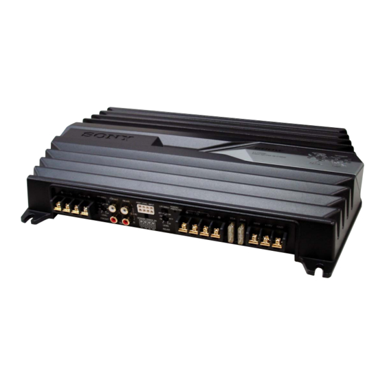
Sony XM-GTX6040 Service Manual
Stereo power amplifier
Hide thumbs
Also See for XM-GTX6040:
- Operating instructions (2 pages) ,
- Specifications (2 pages) ,
- Operating instructions (2 pages)
Table of Contents
Advertisement
SERVICE MANUAL
Ver. 1.0 2009.06
AUDIO POWER SPECIFICATIONS
POWER OUTPUT AND TOTAL HARMONIC DISTORTION
60 watts per channel minimum continuous average power into 4 ohms,
both channels driven from 20 Hz to 20 kHz with no more than 1 % total
harmonic distortion per Car Audio Ad Hoc Committee standards.
Other Specifi cations
Circuit system
OTL (output transformerless) circuit
Pulse power supply
Inputs
RCA pin jacks
High level input connector
Input level adjustment range
0.3 – 6 V (RCA pin jacks),
2.8 – 12 V (High level input)
Outputs
Speaker terminals
2 – 8 Ω (stereo)
Speaker impedance
4 – 8 Ω (when used as a bridging amplifi er)
4 Speakers: 110 W × 4 (at 4 Ω)
Maximum output
3 Speakers: 150 W × 2 (at 2 Ω) +
300 W × 1 (BTL, at 4 Ω)
Rated output (supply voltage at 14.4 V, 20 Hz – 20 kHz, 1 % THD)
4 Speakers:
60 W × 4 (at 4 Ω)
70 W × 4 (at 2 Ω)
Sony Corporation
9-889-574-01
2009F04-1
Audio&Video Business Group
©
2009.06
Published by Sony Techno Create Corporation
XM-GTX6040
SPECIFICATIONS
Frequency response
Harmonic distortion
Low-pass fi lter
High-pass fi lter
Power requirements
Power supply voltage
Current drain
Dimensions
Mass
Supplied accessories
Design and specifi cations are subject to change without notice.
STEREO POWER AMPLIFIER
US Model
Canadian Model
+0
5 Hz – 50 kHz ( dB)
–3
0.05 % or less (at 1 kHz, 4 Ω)
80 Hz, 18 dB/oct
80 Hz, 12 dB/oct
12 V DC car battery (negative ground)
10.5 – 16 V
at rated output: 33 A (4 Ω, 60 W × 4)
Remote input: 1 mA
Approx. 384 × 55 × 252 mm
× 2
× 10 in) (w/h/d) not incl.
(15
1/8
1/4
projecting parts and controls
Approx. 2.9 kg (6 lb 7 oz) not incl. accessories
Mounting screws (4)
High level input cord (1)
Protection cap (1)
Advertisement
Table of Contents

Related Manuals for Sony XM-GTX6040


Summary of Contents for Sony XM-GTX6040
-
Page 1: Service Manual
60 W × 4 (at 4 Ω) 70 W × 4 (at 2 Ω) Design and specifi cations are subject to change without notice. STEREO POWER AMPLIFIER Sony Corporation 9-889-574-01 2009F04-1 Audio&Video Business Group © 2009.06 Published by Sony Techno Create Corporation... - Page 2 PIÈCES SONT CRITIQUES POUR LA SÉCURITÉ DE FONC- WITH MARK 0 ON THE SCHEMATIC DIAGRAMS AND IN TIONNEMENT. NE REMPLACER CES COMPOSANTS QUE THE PARTS LIST ARE CRITICAL TO SAFE OPERATION. PAR DES PIÈCES SONY DONT LES NUMÉROS SONT DON- REPLACE THESE COMPONENTS...
-
Page 3: Table Of Contents
XM-GTX6040 UNLEADED SOLDER TABLE OF CONTENTS Boards requiring use of unleaded solder are printed with the lead- free mark (LF) indicating the solder contains no lead. GENERAL (Caution: Some printed circuit boards may not come printed with Connections ..............the lead free mark due to their particular size) -
Page 4: General
XM-GTX6040 SECTION 1 GENERAL This section is extracted from instruction manual. Connections / Raccordements / Make the terminal connections as illustrated below. Effectuez les connexions des bornes comme illustré ci-dessous. Conexiones Realice las conexiones de terminal como se ilustra a continuación. - Page 5 XM-GTX6040 Input Connections / Connexions d’entrée / Conexiones de entrada Line Input Connection Connexion d’entrée de ligne Conexión de entrada de línea Car audio unit Autoradio Sistema de audio para automóvil LINE OUT LINE OUT Front Rear Avant Arrière Delanteros...
- Page 6 XM-GTX6040 Speaker Connections Turn on or off the LPF and HPF switch at the unit rear as illustrated below. Raccordement des haut-parleurs Réglez le commutateur LPF et HPF situé à l’arrière de l’appareil à On ou Off, comme indiqué dans l’illustration ci-dessous.
-
Page 7: Disassembly
XM-GTX6040 SECTION 2 DISASSEMBLY • This set can be disassembled in the order shown below. 2-1. BOTTOM PLATE (Page 7) 2-2. MAIN BOARD SECTION (Page 8) 2-3. MAIN BOARD (Page 8) Note: Follow the disassembly procedure in the numerical order given. -
Page 8: Main Board Section
XM-GTX6040 2-2. MAIN BOARD SECTION 1 screw (+B, TT, B-type, 3 2 three screws (+P, TT, B-type, 3 3 three screws (+P, TT, B-type, 3 4 three screws (+P, TT, B-type, 3 5 MAIN board section main heat sink 2-3. -
Page 9: Diagrams
XM-GTX6040 SECTION 3 DIAGRAMS THIS NOTE IS COMMON FOR PRINTED WIRING • Note for Replacement of the Transistors The transistors Q110, 111, 210, 211, 310, 311, 410 and 411 have BOARDS AND SCHEMATIC DIAGRAMS. two different ranks: P rank and Y rank. - Page 10 XM-GTX6040 • Waveform • IC Block Diagram IC903 TL594INSR (MAIN Board (2/2)) IC903 5 (CT) 3.3 Vp-p REF 5V ERROR 18 sec 1 V/DIV, 10 sec/DIV ERROR 0.1V...
-
Page 11: Block Diagram
XM-GTX6040 3-1. BLOCK DIAGRAM (FRONT) PRE AMP IC801 (1/2) CN903 OVERLOAD GAIN CONTROL AMP MUTE FRONT CNJ101 (1/2) IC805 (1/2) SWITCH SPEAKER Q112 Q101 VR801-1 DIFFERENTIAL DRIVE DRIVE POWER IC803 (1/2) Q103 Q104 Q108 Q110 MUTE BIAS S801-1 CONTROL Q106,107... -
Page 12: Printed Wiring Board
XM-GTX6040 3-2. PRINTED WIRING BOARD • : Uses unleaded solder. MAIN BOARD (PROTECTOR) (POWER) 1-871-258- D918 S801 S802 POWER/ HPF(80Hz) LPF(80Hz) PROTECTOR VR801 VR802 LEVEL LEVEL (L+R) INPUT HIGH LEVEL INPUT +12V SENSING POWER ON (L+R) REAR SPEAKER OUT FRONT SPEAKER OUT... -
Page 13: Schematic Diagram -Main Section (1/2)
XM-GTX6040 3-3. SCHEMATIC DIAGRAM – MAIN Section (1/2) – R159 R158 R175 D101 R155 Q108 R170 Q104 Q103 C152 Q110 R165 Q112 R167 R177 R163 R112 C151 C153 Q101 VR801 R113 JC726 R153 R161 Q107 IC801(1/2) CNJ101 TP15 R108 C111... -
Page 14: Schematic Diagram -Main Section (2/2)
XM-GTX6040 3-4. SCHEMATIC DIAGRAM – MAIN Section (2/2) – • See page 10 for waveform and IC Block Diagram. (Page 13) R805 C805 Q807 TP22 TP28 Q812 Q811 Q809 Q810 R926 Q911 T901 C819 D803 TP26 R922 Q908 R928 TP23... -
Page 15: Exploded Views
XM-GTX6040 SECTION 4 EXPLODED VIEWS Note: • Items marked “*” are not stocked since • Color Indication of Appearance Parts Ex- The components identifi ed by mark 0 they are seldom required for routine ser- ample: or dotted line with mark 0 are critical for vice. -
Page 16: Main Board Section
XM-GTX6040 4-2. MAIN BOARD SECTION not supplied not supplied Q111, Q110, Q311, Q310, Q211, Q210 Q411, Q410 not supplied F901 D804, D803 F902 Q911, Q910, Q912, Q913 Ref. No. Part No. Description Remark Ref. No. Part No. Description Remark A-1219-711-B... -
Page 17: Electrical Parts List
XM-GTX6040 SECTION 5 MAIN ELECTRICAL PARTS LIST Note: • Due to standardization, replacements in • CAPACITORS When indicating parts by reference num- uF: μF the parts list may be different from the ber, please include the board name. parts specifi ed in the diagrams or the com- •... - Page 18 XM-GTX6040 MAIN Ref. No. Part No. Description Remark Ref. No. Part No. Description Remark C819 1-165-949-41 ELECT 1500uF D904 8-719-083-52 DIODE UDZSUSTE-1716B C820 1-165-949-41 ELECT 1500uF D905 8-719-914-43 DIODE DAN202K C821 1-165-949-41 ELECT 1500uF D906 8-719-914-43 DIODE DAN202K C822 1-165-949-41...
- Page 19 XM-GTX6040 MAIN Ref. No. Part No. Description Remark Ref. No. Part No. Description Remark Q103 8-729-014-87 TRANSISTOR 2SC4207(T5RSONY,F) Q905 8-729-052-82 TRANSISTOR KTA1281Y-AT Q104 8-729-140-82 TRANSISTOR 2SA988-PAFAEA Q906 8-729-120-28 TRANSISTOR 2SC1623-L5L6 Q105 8-729-140-84 TRANSISTOR 2SC1841-PAFAEA Q907 8-729-027-43 TRANSISTOR DTC114EKA-T146 Q106 8-729-041-66...
- Page 20 XM-GTX6040 MAIN Ref. No. Part No. Description Remark Ref. No. Part No. Description Remark R209 1-218-882-11 METAL CHIP 0.5% 1/10W R367 1-216-134-00 METAL CHIP 1/8W R210 1-218-871-11 METAL CHIP 0.5% 1/10W R368 1-216-134-00 METAL CHIP 1/8W R211 1-218-871-11 METAL CHIP 0.5%...
- Page 21 XM-GTX6040 MAIN Ref. No. Part No. Description Remark Ref. No. Part No. Description Remark R812 1-216-837-11 METAL CHIP 1/10W < THERMISTOR > R813 1-216-837-11 METAL CHIP 1/10W R814 1-216-210-00 METAL CHIP 3.3K 1/8W TH901 1-801-597-11 THERMISTOR R815 1-216-210-00 METAL CHIP 3.3K...
-
Page 22: Revision History
XM-GTX6040 REVISION HISTORY Checking the version allows you to jump to the revised page. Also, clicking the version at the top of the revised page allows you to jump to the next revised page. Ver. Date Description of Revision 2009.06...