Sony XES-Z50 Service Manual
Digital reference sound system
Hide thumbs
Also See for XES-Z50:
- Operating instructions manual (64 pages) ,
- Operating instructions manual (72 pages) ,
- Service manual (152 pages)
Table of Contents
Advertisement
SERVICE MANUAL
Ver 1.1 2001.09
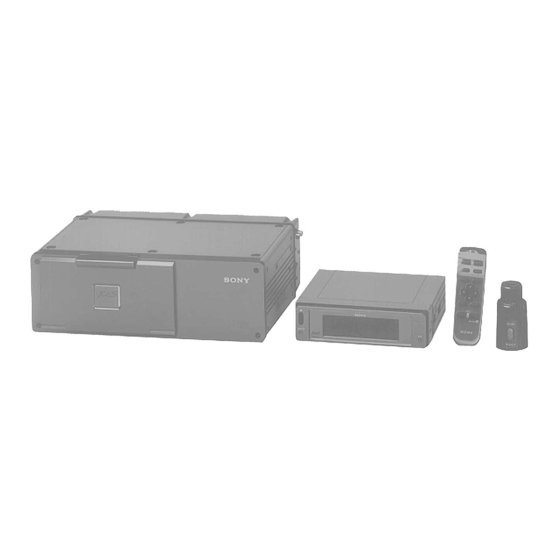
• This set consists of the following units.
CHANGER UNIT
CONTROL UNIT
WIRELESS REMOTE COMMANDER (RM-X67)
ROTARY REMOTE COMMANDER (RM-X66)
Sony Corporation
9-925-509-12
2001I0500-1
e Vehicle Company
C 2001.9
Shinagawa Tec Service Manual Production Group
XES-Z50
Model Name Using Similar Mechanism
CD Mechanism Type
Optical Pick-up Name
SPECIFICATIONS
DIGITAL REFERENCE SOUND SYSTEM
US Model
Canadian Model
NEW
MG-110ES-132
KSS-400A
– Continued on next page –
Advertisement
Table of Contents

Related Manuals for Sony XES-Z50


Summary of Contents for Sony XES-Z50
- Page 1 XES-Z50 SERVICE MANUAL US Model Canadian Model Ver 1.1 2001.09 • This set consists of the following units. Model Name Using Similar Mechanism CHANGER UNIT CD Mechanism Type MG-110ES-132 CONTROL UNIT Optical Pick-up Name KSS-400A WIRELESS REMOTE COMMANDER (RM-X67) ROTARY REMOTE COMMANDER (RM-X66) SPECIFICATIONS –...
- Page 2 SONY PARTS WHOSE PART NUMBERS APPEAR AS DE FONCTIONNEMENT. NE REMPLACER CES COM- SHOWN IN THIS MANUAL OR IN SUPPLEMENTS PUB- POSANTS QUE PAR DES PIÈCES SONY DONT LES LISHED BY SONY. NUMÉROS SONT DONNÉS DANS CE MANUEL OU DANS LES SUPPLÉMENTS PUBLIÉS PAR SONY.
-
Page 3: Table Of Contents
TABLE OF CONTENTS SERVICING NOTES DIAGRAMS 1-1. Connection at Repair ............ 7-1. IC Pin Function Description ......... 1-2. Front Panel Setting ............7-2. IC201 (BA6247FP-Y) Motor Driver IC Operation ..76 1-3. Removal of Front Panel at Power Off ......7-3. -
Page 4: Servicing Notes
SECTION 1 SERVICING NOTES 1-1. CONNECTION AT REPAIR 1-2. FRONT PANEL SETTING In repairing this set, connect as follows. In repairing the front panel, make a setting through the procedure give below. regulated dc Notes: CN501 power supply 1. A flat cable and a switch flexible board connected between power supply 14.4 V dc connector... -
Page 5: General
SECTION 2 This section is extracted from instruction manual. GENERAL – 5 –... - Page 6 – 6 –...
- Page 7 – 7 –...
- Page 8 – 8 –...
- Page 9 – 9 –...
- Page 10 – 10 –...
- Page 11 – 11 –...
- Page 12 – 12 –...
- Page 13 – 13 –...
- Page 14 – 14 –...
- Page 15 – 15 –...
- Page 16 – 16 –...
- Page 17 – 17 –...
- Page 18 – 18 –...
- Page 19 – 19 –...
- Page 20 – 20 –...
- Page 21 – 21 –...
- Page 22 – 22 –...
- Page 23 – 23 –...
- Page 24 – 24 –...
- Page 25 – 25 –...
- Page 26 – 26 –...
- Page 27 – 27 –...
- Page 28 – 28 –...
- Page 29 – 29 –...
- Page 30 – 30 –...
- Page 31 – 31 –...
- Page 32 – 32 –...
- Page 33 – 33 –...
- Page 34 – 34 –...
- Page 35 – 35 –...
- Page 36 – 36 –...
-
Page 37: Disassembly
SECTION 3 DISASSEMBLY • This set can be disassembled in the order shown below. CHANGER SECTION FRONT/SIDE/ MECHANISM EV SECTION, ROLLER (T), DSP ASS’Y COVER COVER (MDEK) (Page 37) (UPPER • REAR PANEL DECK SECTION CHASSIS (MZ,EK) DPT BOARD, ASS’Y, ESCUTCHEON (2) ARM (KR) LOWER) (Page 38) - Page 38 4 cover (upper • lower) [COVER (UPPER • LOWER) ] 2 three screws (M 3 × 6) 2 three screws (M 3 × 6) 3 three spacers (cover) 3 three spacers (cover) 1 seal (DSP) 6 three spacers (cover) 7 cover (upper • lower) 5 three screws (M 3 ×...
- Page 39 [MECHANISM DECK SECTION (MG-110ES-132) ] 2 chassis (TOP) 1 two screws (BVTT 2.6 × 4) 3 two screws (P 2.6 × 4) 1 three screws (BVTT 2.6 × 4) 4 cover (damper L) 6 tension spring (FL2) 3 three screws (P 2.6 ×...
- Page 40 [COVER (MDEK) ASS’Y, ESCUTCHEON (2)] 1 two screws (PTT 2 × 4) 1 four screws (PTT 2 × 4) 4 cover (MDEK) ass’y 1 two screws (PTT 2 × 4) 2 tension spring (EV) 3 two claws 6 escutcheon (2) 5 claw [DRIVER BOARD, OPTICAL PICK-UP (KSM-400AAM) ] 4 three screws...
- Page 41 [EV SECTION, CHASSIS (MZ, EK) ASS’Y] 4 rack (110) 3 screw (PTT 2 × 4) 6 four screws (PTT 2 × 4) 5 EV section 1 two washers 2 lever (X) ass’y 7 chassis (MZ, EK) ass’y 1 two washers 2 lever (X) ass’y 2 lever (X) ass’y 1 two washers...
- Page 42 CONTROLLER SECTION [FRONT PANEL ASS’Y] 1 screw (PTT 2.6 × 6) 2 case (lock upper) 3 Turn the gear (A) to direction of the arrow A . 1 three screws (PTT 2.6 × 6) 4 front panel ass’y [LIQUID CRYSTAL MODULE] 1 two screws (P 2 ×...
- Page 43 [SUB PANEL ASS’Y, FRONT PANEL DESORPTION MACHINERY] 6 front panel desorption machinery 1 two screws (P 2.6 × 6) 5 sub panel ass’y tuner control section 2 two screws (PTT 2.6 × 10) 1 two screws (P 2.6 × 6) 3 connector (CN53) 4 two connectors...
- Page 44 [TUNER ASS’Y] 2 chassis (main upper) 1 two screws (PTT 2.6 × 6) 4 two connectors (CN505, 509) 3 screw (PTT 2.6 × 6) 8 two connectors (CN506, 507) 5 two screws (B 2.6 × 10) 1 four screws (PTT 2.6 × 6) 6 two spacers 7 tuner ass’y 5 two screws...
-
Page 45: Mechanical Adjustment
SECTION 4 MECHANICAL ADJUSTMENT 2. Fit the rack assembly putting it in the arrow A direction. At 4-1. ELEVATOR HEIGHT ADJUSTMENT this time insert a spacer (approx. 1 mm thickness) or fit the rack assembly while pushing the EV chassis assembly in the This adjustment should be done when replacing the rack assem- arrow B direction. -
Page 46: Test Mode
SECTION 5 TEST MODE This set have the test mode function. In the test mode, FM Auto FM AUTO SCAN/STOP LEVEL ADJUSTMENT Scan/Stop Level and AM Auto Scan/Stop Level adjustments can Setting: be performed easier than it in ordinary procedure. TUN/AUX button: FM FM RF signal Setting the Test Mode... - Page 47 AM AUTO SCAN/STOP LEVEL ADJUSTMENT FM STEREO SEPARATION ADJUSTMENT Setting: Note: Make this adjustment after “FM AUTO SCAN/STOP TUN/AUX button : FM LEVEL ADJUSTMENT”. Setting: FM RF signal level meter TUN/AUX button: AM antenna (MAIN) terminal generator 0.01 µ F 10 k Ω...
-
Page 48: Cd Section
TRACKING OFFSET ADJUSTMENT CD SECTION Condition: This adjustment is performed with the set place hori- zontally. Notes: Connection: 1. Perform adjustments in the order given. 2. Use YEDS-18 disc (Part No.: 3-702-101-01) unless otherwise oscilloscope indicated. (DC range) 3. Use the oscilloscope with more than 10 MΩ impedance. DRIVER board 4. -
Page 49: Display Section
DISPLAY SECTION CONTRAST ADJUSTMENT Note on adjustment: Adjust the contrast at “8” of 15 steps. Connection: digital voltmeter liquid crystal module – Adjustment Procedure: 1. Fix display board and rear panel with screws. 2. Connect the display board and liquid crystal module. 3. - Page 50 CONNECTION AND ADJUSTMENT LOCATION • TUNER Section – Control Unit (FM/AM Tuner Unit) – AM AUTO SCAN/STOP LEVEL Adjustment RV201 FM STEREO SEPARATION Adjustment RV204 FM AUTO SCAN/STOP LEVEL Adjustment RV203 front side FM NOISE FOCUS Adjustment RV205 • CD Section –...
- Page 51 • DISPLAY Section – Liquid Crystal Module – – DISPLAY Board (Conductor Side) – CN502 CONTRAST Adjustment RV801 – 51 –...
-
Page 52: Diagrams
BUS ON SONY bus), and FM character multiple broadcast display controller (IC802) ÒLÓ: bus on Reset signal output to the tuner controller (IC502), bus interface (IC503) (for SONY bus), and SYS RST FM character multiple broadcast display controller (IC802) ÒLÓ: reset... - Page 53 SIRCS Sircs signal input from the remote control receiver in display unit BU IN Backup power supply detect signal input from the bus interface (IC503) (for SONY bus) ACC IN Accessory power supply detect signal input terminal “L”: accessory on...
- Page 54 Pin No. Pin Name Function Input of acknowledge signal for key input Input of acknowledge signal to accept FUNCTION KEY ACK and EJECT keys when the power is in off status ON at “L” input Input of auxiliary input (AUX IN) on/off detection Input terminal to turn on the set AUX ON simultaneously when an external unit connected to the AUX IN terminal is turned on, if the power of the set is off “L”: When external unit is turned on...
- Page 55 PLL chip enable signal output to the FM/AM tuner unit Communication request signal output to the bus interface (IC503) (for SONY bus) UNIREQ “H”: communication request LINK OFF Bus on/off control signal output of the bus interface (for SONY bus) Not used (open) – 55 –...
- Page 56 Function UNICKI Serial data transfer clock signal input from the system controller (IC501) UNISI Serial data input from the bus interface (IC503) (for SONY bus) UNISO Serial data output to the bus interface (IC503) (for SONY bus) — Power supply terminal (+5V) AVDD —...
- Page 57 Ground terminal LCD-TX Transmit data output to the display controller (IC901) UNISO Serial data output to the bus interface (IC503) (for SONY bus) LCD-RX Receive data input from the display controller (IC901) UNISI Serial data input from the bus interface (IC503) (for SONY bus)
- Page 58 SYSRES “L”: reset For several hundreds msec. after the power supply rises, “L” is input, then it changes to “H” BU-IN Backup power supply detection signal input from the bus interface (IC503) (for SONY bus) — Ground terminal EXTAL System clock input terminal (14.745 MHz) XTAL System clock input terminal (14.745 MHz)
- Page 59 Output of power on/off control signal for the back light in display unit “H”: power on LINK-OFF Bus on/off control signal output to the bus interface (IC503) (for SONY bus) “L”: bus on Output of power on/off control signal for the external device DEC-ON “H”: power on Not used (open)
- Page 60 DISPLAY BOARD IC901 HD6473048-DISP01 (DISPLAY CONTROLLER) Pin No. Pin Name Function — Power supply terminal (+5V) LED drive signal output for the TIR indicator “H”: LED on Not used Not used (open) Output of command transmission start control signal to the LCD controller for liquid crystal module The OR signal with the busy signal from LCD controller for liquid crystal module is input to the LCD-BUSY (pin 9) LCD-START...
- Page 61 Pin No. Pin Name Function Address signal output to the flash memory (IC931) and S-RAM (IC932) — Ground terminal Address signal output to the flash memory (IC931) and S-RAM (IC932) — Ground terminal Not used (fixed at “H”) Not used (open) Not used (open) Ø...
- Page 62 Pin No. Pin Name Function Not used (fixed at “L”) CONTR Contrast alignment signal output to the liquid crystal module (D/A output) DIMER Back light brightness control signal output to the liquid crystal module (D/A output) AVSS — Ground terminal (for A/D conversion) Not used (open) SRAM-CS Chip enable signal output to the S-RAM (IC932)
- Page 63 Not used (open) System reset signal input from the reset signal generator (IC903) and bus interface (IC951) (for RESET SONY bus) “L”: reset For several hundreds msec. after the power supply rises, “L” is input, then it changes to “H” XTLI...
- Page 64 Serial data output to the CD text decoder (IC303) Serial data input from the CD text decoder (IC303) Serial data transfer clock signal input from the bus interface (IC951) (for SONY bus) Serial data input from the bus interface (IC951) (for SONY bus)
- Page 65 Pin No. Pin Name Function Guard frame sync signal input from the digital signal processor (IC501) “L”: NG, “H”: OK SENS Count sense signal input from the digital signal processor (IC501) — — Not used (open) — *1 Elevator up/down motor, disc load/save motor control Operation Elevator up/down motor (M501) Disc load/save motor (M502)
- Page 66 DATA7 System reset signal input from the system controller (IC301), reset signal generator (IC903), and bus interface (IC951) (for SONY bus) “L”: reset For several hundreds msec. after the power supply rises, “L” is input, then it changes to “H”...
- Page 67 Pin No. Pin Name Function — Power supply terminal (+5V) Not used (open) Not used (fixed at “L”) Not used (fixed at “H”) ADD14 Address signal output to the S-RAM (IC304) ADD15 Address signal output to the S-RAM (IC304) SCOR Subcode sync (S0+S1) detection signal input from the digital signal processor (IC501) WFCK Write frame clock (7.35 kHz) signal input from the digital signal processor (IC501)
- Page 68 IC101 CXD2711Q (DIGITAL SIGNAL PROCESSOR FOR FRONT/REAR SPEAKER) DSP BOARD IC201 CXD2711Q (DIGITAL SIGNAL PROCESSOR FOR SUB-WOOFER SPEAKER) Pin No. Pin Name Function — Ground terminal Output of ready signal at serial data transfer to the master controller (IC301) CRDY The start cause interruption occurs by a falling edge CCNT Input of control/data from address bus for the master controller (IC301) “L”: data input...
- Page 69 Pin No. Pin Name Function Serial audio data output terminal IC101: Serial data (for front speaker) output terminal IC201: Serial data (for sub-woofer speaker) output terminal Serial audio data output terminal IC101: Serial data (for rear speaker) output terminal IC201: Not used (open) —...
- Page 70 Pin No. Pin Name Function MA13 MA14 Address signal output terminal Not used (open) MA15 — Ground terminal MA00 IC101: Address signal output to the D-RAM (IC102) IC201: Address signal output to the D-RAM (IC202) MA01 — Ground terminal MA02 IC101: Address signal output to the D-RAM (IC102) IC201: Address signal output to the D-RAM (IC202) MA03...
- Page 71 Serial data input from the bus interface (IC306) (for SONY bus) Not used (fixed at “L”) UNICKI Serial data transfer clock signal input from the bus interface (IC306) (for SONY bus) Two-way data bus with the flash memory (IC401) —...
- Page 72 Standby signal input terminal Fixed at “H” in this set System reset signal input from the reset signal generator (IC303) and bus interface (IC306) (for SYSRES SONY bus) “L”: reset For several hundreds msec. after the power supply rises, “L” is input, then it changes to “H” BU-IN Backup power supply detect signal input terminal (used also to reset standby) —...
- Page 73 Serial data input from the digital signal processor (IC601 CXD2710R) AVSS — Ground terminal (for A/D conversion) Bus on/off control signal input from the bus interface (IC306) (for SONY bus) “L”: bus on BUS-ON With the bus in off status, standby is cancelled by bus on falling edge 2711-CE...
- Page 74 DSP BOARD IC601 CXD2710R (DIGITAL SIGNAL PROCESSOR) Pin No. Pin Name Function AMPIN Loop filter amplifier input for the PLL Not used (fixed at “L”) AMPOUT Loop filter amplifier output for the PLL Not used (open) — Power supply terminal (+5V) —...
- Page 75 Pin No. Pin Name Function 58 to 64 TEST Not used (open) — Ground terminal 66 to 74 TEST Not used (open) EBDIR Not used (fixed at “L”) UBDIR Not used (fixed at “L”) D.SEL1 Input terminal for data output setting serial out or parallel out (fixed at “L”) —...
-
Page 76: Ic201 (Ba6247Fp-Y) Motor Driver Ic Operation
7-2. IC201 (BA6247FP-Y) MOTOR DRIVER IC OPERATION (DRIVER BOARD) The elevator up/down motor connected between pin @™ and pin !• of IC201 is as M501, and the disc load/save motor connected between pin 1 and pin !• of IC201 is as M502. When the IC port logic is pin @™... -
Page 77: Block Diagram - Control Unit (Tuner Section)
XES-Z50 XES-Z50 7-3. BLOCK DIAGRAM – CONTROL UNIT (TUNER Section) – CN502 • Signal path. (1/2) L-CH –1 : FM L-CH (ANTENNA) TO CD : AM CHANGER R-CH –2 MAIN R-CH (FM/AM) MUTE MAIN ANT Q605, 606 FM/AM SUB (FM) -
Page 78: Block Diagram - Control Unit (Display Section)
XES-Z50 7-4. BLOCK DIAGRAM – CONTROL UNIT (DISPLAY Section) DISPLAY CONTROLLER DISPLAY CONTROLLER LIQUID CRYSTAL IC802 (1/2) IC901 DISPLAY MODULE SIRCS LEVEL SHIFT BUFFER SIRCS (Page 81) LCD-RX TX-LCD IC509 IC942 (1/2) D8 – D15 D0 – D15 D0 – D15... -
Page 79: Block Diagram - Control Unit (Bus Control/Power Supply Section)
D540 IC502 (2/2) SIRCS REMOTE IN SWITCH AUX-ON Q530 D507 ACCESSORY CHECK ACCESSORY Q520 BUS INTERFACE RESET BATTERY (FOR SONY BUS) SWITCH SWITCH IC503 44 14 16 ANT-REM D520 ANTENNA REMOTE SWITCH BATTERY CHECK LEVEL SHIFT Q503, 504 SWITCH Q518... -
Page 80: Block Diagram - Changer Unit (Cd Section (1/2))
XES-Z50 7-6. BLOCK DIAGRAM – CHANGER UNIT (CD Section (1/2)) – FILTER RF AMP, DATA, FOCUS/TRACKING ERROR AMP 20 22 BCLK IC101 DATA (Page 85) DIGITAL SIGNAL BCLK PROCESSOR GTOP IC501 SERIAL/ PARALLEL RFCK GTOP, DIGITAL PLL PROCESSOR RFCK, RAOF... -
Page 81: Block Diagram - Changer Unit (Cd Section (2/2))
XES-Z50 7-7. BLOCK DIAGRAM – CHANGER UNIT (CD Section (2/2)) – • Signal path. D-RAM CONTROLLER : CD PLAY IC401 DIGITAL D OUT DATA, DATA, BCLK DATA DATAI (Page 84) BCK, LRCK DATA DATA DIGITAL (Page 87) BCLK BCKI SIGNAL... -
Page 82: Block Diagram - Changer Unit (Main Section (1/2))
XES-Z50 7-8. BLOCK DIAGRAM – CHANGER UNIT (MAIN Section (1/2)) – DATA DATA CN12 (1/2) BCK, LRCK DATA DATA (Page 86) (Page 89) IC417 MASTER BUS ISOLATION CONTROLLER BUFFER IC702, LRCK, BCK IC701 (1/2) (Page 89) IC703 (1/2) LRCK LRCK... -
Page 83: Block Diagram - Changer Unit (Main Section (2/2))
XES-Z50 7-9. BLOCK DIAGRAM – CHANGER UNIT (MAIN Section (2/2)) – LRCK, BCK (Page 91) (Page 88) DATA (HIGH FRONT) S1DI CD S1OUT DATA S2DI DIR DIGITAL SIGNAL PROCESSOR DATA LEVEL (FOR HIGH FRONT, MID REAR SPEAKER) (MID REAR) S3DI AD... -
Page 84: Changer Unit (D/A Converter Section)
XES-Z50 7-10. BLOCK DIAGRAM – CHANGER UNIT (D/A CONVERTER Section) – DIGITAL FILTER D/A CONVERTER IC1101 LINE OUT IC1102 HIGH (3WAY) DATA FRONT (4CH) ELECTRICAL VOLUME (HIGH FRONT) (Page 90) FILTER/ IC1106 INPUT DATA ATTENUATOR DATA JK3011 (MID REAR) BCKI... -
Page 85: Block Diagram - Changer Unit (Bus Control/Power Supply Section)
XES-Z50 7-11. BLOCK DIAGRAM – CHANGER UNIT (BUS CONTROL/POWER SUPPLY Section) – CN13 SONY BUS CONTROL CN11 +18V +15V POWER +15V/–15V REGULATOR –18V IC1501, 1502 L801 D804 –15V RESET SIGNAL SCHMITT A/D, D/A DC/DC 63 SYSRST GENERATOR TRIGGER CONVERTER CONVERTER... -
Page 86: Control Unit (Main Section)
XES-Z50 • Circuit Boards Location – CHANGER UNIT – – CONTROL UNIT – LINE OUT board DAC board DPT board TRANSLATION board OPEN/CLOSE 1 board OPEN/CLOSE 2 board DISPLAY board LINE IN board DSP board SW board FM/AM TUNER assy... - Page 99 • Waveforms – CONTROL UNIT (MAIN Board) – 6 IC501 &™ (XT2) 1 IC802 ^§ (EXTAL) 2.2 Vp-p 3.2 Vp-p 31 µ s 68 ns 2 IC802 ^¶ (XTAL) 7 IC501 &º (X1) 3.1 Vp-p 3.4 Vp-p 68 ns 198 ns 3 IC502 8 (X1) 8 IC501 ^ª...
-
Page 100: Changer Unit (Driver Section)
– CONTROL UNIT (DISPLAY Section) – – CHANGER UNIT (DRIVER Board) – 1 PH21 COLLECTOR 1 IC101 !¢ (TE) (Front panel is being removed or attached.) 5.3 Vp-p Approx. 920 mVp-p Approx. 100 ms 2 IC101 !§ (FE) 2 IC901 ^§ (EXTAL) Approx. -
Page 101: Changer Unit (Changer Section)
– CHANGER UNIT (CHANGER Board) – 6 IC251 4, 6 1 IC601 3 (RF) 6 IC501 @¢ (RF) 2.6 Vp-p Approx. +0.3 Vp-p 1.1 Vp-p –0.2 3.8 µ s 2 IC601 4 (TE) 7 IC401 !£ (WDCI), IC501 #¡ (WDCK) Note: DRIVER board waveforms are CD play mode. - Page 102 !¡ IC401 3 (WFCK), IC501 ^™ (WFCK) !§ IC501 %• (C16M) @¡ IC303 @ª (EXTAL) 4.7 Vp-p 5.2 Vp-p 3.1 Vp-p 136 µ s 59 ns 99 ns !™ IC501 %¢ (XTAO) !¶ IC503 0 (CKO) @™ IC303 #º (XTAL) 4.3 Vp-p 4.1 Vp-p 5.4 Vp-p...
-
Page 103: Changer Unit (Changer Section)
– CHANGER UNIT (DSP Board) – 1 IC701 !™ (BCK IN) 6 IC703 !¢ (SYNC) !¡ IC601 (∞ (LRCK) NOTE 1 5.1 Vp-p 5.2 Vp-p 5.3 Vp-p 22.7 µ s 474 ns CD PLAY, FM/AM, AUX ANALOG AUDIO MODE: 22.7 µ s 2 IC701 3 (SYNC OUT) NOTE 1 7 IC502 !¡... -
Page 104: Changer Unit (Dsp Section)
– CHANGER UNIT (DAC Board) – !§ IC101, 201 #¢ (LRCK) 5 IC1101, 1201, 1301 6 (XTI) NOTE 2 1 IC1010 2 (MCK IN) NOTE 1 5 Vp-p 3.5 Vp-p 6 Vp-p 89 ns CD PLAY, FM/AM, AUX ANALOG 358 ns AUDIO MODE: 22.7 µ... - Page 105 9 IC1101, 1201, 1301 @§ (BCKO) NOTE 1 !£ IC1401 2 (1A) !• IC1402 6 (1QD) 5.2 Vp-p 5.1 Vp-p 5.2 Vp-p 354 ns 89 ns 1.42 µ s 0 IC1101, 1201, 1301 @∞ (WCKO) !¢ IC1401 5 (2A) !ª IC1402 8 (2QD) NOTE 1 5.2 Vp-p 5.2 Vp-p...
- Page 106 @£ IC1607 !§ (FSYNC) NOTE 3 5.3 Vp-p 11.35 µ s @¢ IC1607 !ª (CLK) NOTE 2 6 Vp-p 89 ns @∞ IC1607 !ª (CLK) NOTE 1 6.5 Vp-p 354 ns Notes: 1. AUX DIGITAL AUDIO mode. 2. CD PLAY, FM/AM, and AUX ANALOG AUDIO mode. 3.
-
Page 107: Ic Block Diagram
• IC Block Diagram – MAIN Board – IC503 MM1175XF-T1 BUS ON RESET RESET RESET SWITCH BUS ON BATT BATT SWITCH BATT VREF CHECK DATA DATA IN IN/OUT DATA OUT IC516 AT24C08N-10SI-SL383B IC515 NM24C04EM8-FL63 START CYCLE H.V. GENERATION TIMING & CONTROL START/ START STOP... - Page 108 IC804 MBM29F400BA-70PFTN-MA02 BYTE DQ15/A–1 4,194,304 CELL DECODER MATRIX DQ14 Y GATE DQ13 ADDRESS BUFFER LATCH DATA DQ12 DECODER LATCH DQ11 DQ10 CONTROL LOW VCC CIRCUIT DETECTOR CIRCUIT RESET WRITE/ERASE PULSE TIMER RY/BY WRITE CIRCUIT RY/BY ERASE CIRCUIT BUFFER CHIP ENABLE/ OUTPUT ENABLE CIRCUIT IC805 CXK516100TM-70LL-TL...
- Page 109 – DISPLAY Board – IC801 TL5001CD U.V.L.O DEAD-TIME REFERENCE COMPARATOR VOLTAGE – SWITCH ERROR 'ON' – S.C.P. – COMPARATOR 1 COMPARATOR – S.C.P. LATCH S.C.P. COMPARATOR 2 IC931 MBM29F800-DISPU BYTE DQ15/A–1 8,388,608 CELL DECODER MATRIX DQ14 Y GATE DQ13 ADDRESS BUFFER LATCH DQ12...
- Page 110 IC932 CXK516100TM-70LL-TL LEVEL SHIFT & CONTROL I/O16 BUFFER I/O1 I/O15 I/O2 I/O14 I/O3 I/O13 I/O4 MEMORY MEMORY MATRIX MATRIX DECODER 512 x 1024 512 x 1024 I/O5 I/O6 I/O12 I/O7 I/O11 I/O GATE I/O GATE I/O8 COLUMN COLUMN I/O10 BUFFER DECODER BUFFER DECODER...
-
Page 111: Driver Board
– DRIVER Board – IC101 CXA1791M-T6 IC201 BA6247FP-Y OUT3 DRIVER VREF LD AMP PD AMP 1.25V 20 VCC – – 22 OUT2 DRIVER 19 APC ON 20 GND 18 RFI 19 GND – – VCC1 17 RFO IV AMP1 SUMMING AMP 18 OUT1 DRIVER 16 VCC2... - Page 112 – CHANGER Board – IC401 CXD2512AQ IC302 AT24C32N-10SI-TR START/ STOP LOGIC H.V. GRSRST 64 SDTO SUBQ TBC SERIAL PUMP/ CPU I/F LOAD 63 XSOE XRST CONTROL DEVICE CONTROL TIMING COMP ADDRESS LOGIC WFCK 62 SCK DATA COMPARATOR SDTI LINKING EXPXLT CONTROL DATA XROI...
- Page 113 IC402, 403 µPD424400GS-60-9JD CLOCK OSC A0–A9 XRAS XCAS COLUMN DECODER SENSE REFRESH AMP INPUT/OUTPUT CONTROL SWITCH MEMORY CELL IC501 CXD2540Q 56 55 47 46 DIGITAL CLOCK TIMING SUBCODE GENERATOR GENERATOR 2 EXCK SERIAL/PARALLEL PROCESSOR PROCESSOR TIMING PEAK XUGF GENERATOR 1 DETECTOR 39 DYOP 38 64LRCK...
- Page 114 IC502 SN74HC74ANS IC951 MM1284XFFE 13 12 11 BUS ON OUT BUS ON INPUT BUS ON LINK OFF CLK OUT BUS CLK VREF BUS DATA DATA OUT DATA IN 1 2 3 4 5 6 RESET BUS RESET RESET IC503 TC9246F-TP1 –...
- Page 115 – DSP Board – IC102, 202 HM51W4260CLTT-7 IC302 AT24C32N-10SI-TR START/ STOP LOGIC H.V. ADDRESS BUS I/O BUS SERIAL PUMP/ LOAD DEVICE CONTROL TIMING COMP 256K MEMORY ADDRESS LOGIC ARRAY MAT DECODER COMPARATOR I/O BUFFER I/O BUS AND DATA SELECTOR COLUMN DECODER RECOVERY DATA WORD EEPROM...
- Page 116 IC415 TC74VHC595FS (EL) SHIFT REGISTER LATCH PARALLEL DATA OUTPUT IC502 CS8412-IS-E1 VERF CE/F2 CD/F1 MULTIPLEXER CC/F0 PARITY CB/E2 CHECK CA/E1 C0/E0 FREQUENCY CHANNEL ERROR ENCODER SDATA STATUS LATCH COMPARATOR CHECK REGISTERS DGND AGND BI-PHASE MULTIPLEXER FILT DECODER AND CONFIDENCE AUDIO FRAME SYNC FLAG SERIAL...
- Page 117 – DAC Board – IC1101, 1201, 1301 SM5843AS1-ET OUTPUT DATE DE-EMPHASIS INTERFACE CONTROL OP ATTENUATION BLOCK TIMING CONTROL INPUT DATA INTERFACE MUTE/ATTENUATOR SYSTEM CLOCK CONTROL IC1102, 1103, 1202 PCM1702U-K-T1 IC1203, 1302, 1303 IC1106, 1206, 1306 CS3310-KP AINL –VCC DATA – AGNDL INPUT INTERFACE...
- Page 118 IC1401 TC74VHC125F (EL) IC1606 TC7W74FU 14 VCC 1 OE 4 OE 2 OE 3 OE IC1607 AK5390-VS AGND VREF+ VOLTAGE REFERENCE VREF– AINR+ AINL+ AINR– + – + – AINL– ACAL – – LGND VA– FILTER FILTER IC1402 TC74VHC393F (EL) + –...
-
Page 119: Exploded Views
SECTION 8 EXPLODED VIEWS NOTE: • -XX and -X mean standardized parts, so they • Items marked “*” are not stocked since they The components identified by mark ! or dotted line with mark ! are may have some difference from the original are seldom required for routine service. - Page 120 (2) CD CHANGER MAIN SECTION-2 JK3011, 3021, 3031 JK3012, 3022, 3032 supplied with JK3011, 3021, 3031 supplied with JK3021, 3022, 3032 supplied with JK2012 supplied with JK2011 JK2012 JK2011 Ref. No. Part No. Description Remark Ref. No. Part No. Description Remark 3-906-712-01 SCREW (2.6X6) (CU), +PTT * 70...
- Page 121 (3) CD CHANGER MAIN SECTION-3 Ref. No. Part No. Description Remark Ref. No. Part No. Description Remark 3-923-342-01 SPRING (FL2), TENSION * 114 3-015-118-01 SHEET (CD INNER CHASSIS. REAR S) 3-375-501-01 DAMPER (CNG) * 115 3-015-116-01 SHEET (CD INNER CHASSIS. FRONT) * 103 3-008-203-01 COVER (DAMPER L) * 116...
- Page 122 (4) CD CHANGER MAIN SECTION-4 MG-110ES-132 KSM-400AAM not supplied Ref. No. Part No. Description Remark Ref. No. Part No. Description Remark * 151 A-3309-668-A DRIVER BOARD, COMPLETE * 160 3-008-217-01 BRACKET (FPC) * 152 1-664-111-12 SW BOARD 1-664-155-11 RF FLEXIBLE BOARD 1-664-157-11 SWITCH FLEXIBLE BOARD 1-664-156-11 DRIVER FLEXIBLE BOARD * 154...
- Page 123 (5) MECHANISM DECK SECTION-1 (MG-110ES-132) not supplied Ref. No. Part No. Description Remark Ref. No. Part No. Description Remark 3-911-104-01 WASHER * 207 X-3372-963-1 COVER (MDEK) ASSY 3-013-099-01 SPRING (EJES) 3-931-995-01 SPRING (EV), TENTION X-3371-264-1 LEVER (NET) ASSY 3-931-453-01 RACK (110) 3-927-978-01 SPRING, TENSION 3-930-600-01 RACK (EV) * 205...
- Page 124 (6) MECHANISM DECK SECTION-2 (MG-110ES-132) M801 Ref. No. Part No. Description Remark Ref. No. Part No. Description Remark 3-911-105-11 CUSHION (M) 3-377-720-01 WASHER, POLYETHYLENE 3-911-090-01 WHEEL (B2), WORM 3-379-490-11 WASHER, POLYETHYLENE 3-911-076-11 GEAR (MS) 3-568-315-01 SPRING, COMPRESSION 3-927-977-01 SPRING, COMPRESSION * 267 3-911-093-01 SHAFT (SDR2) 3-908-794-01 LEVER (T2) (MZ LOCK)
- Page 125 (7) MECHANISM DECK SECTION-3 (MG-110ES-132) 309 310 not supplied Ref. No. Part No. Description Remark Ref. No. Part No. Description Remark * 301 3-930-565-01 BRACKET (DPTT) X-3371-483-1 ARM (DHK2) ASSY 3-364-421-01 BEARING (ROLLER) 3-932-166-01 SPRING 3-701-438-11 WASHER, 2.5 X-3371-484-1 BRACKET (CPK) ASSY 3-909-408-01 ROLLER (T) 3-915-913-01 PLATE (CD), CHUCK * 305...
- Page 126 (8) MECHANISM DECK SECTION-4 (MG-110ES-132) M502 M501 SW501 PRG401 Ref. No. Part No. Description Remark Ref. No. Part No. Description Remark * 351 X-3371-260-1 CHASSIS (EVT) ASSY 3-930-568-02 BRACKET (EVMT) 3-911-087-01 LOCK (CLAW) 3-388-479-01 SPRING, COMPRESSION 3-911-097-01 SHAFT (LOCK 2) 3-930-298-01 WASHER (TEFLON) 3-308-717-00 SPRING, COMPRESSION 3-377-719-01 WASHER, POLYETHYLENE...
- Page 127 (9) OPTICAL PICK-UP SECTION (KSM-400AAM) The components identified by Les composants identifiés par une mark ! or dotted line with marque ! sont critiques pour la mark ! are critical for safety. sécurité. Replace only with part number Ne les remplacer que par une pièce specified.
- Page 128 (10) MASTER CONTROL UNIT not supplied not supplied F501 front panel desorption machinery tuner control section Ref. No. Part No. Description Remark Ref. No. Part No. Description Remark X-3372-942-1 PANEL (ORNAMENT) ASSY, FRONT * 467 3-014-062-01 CUSHION (PLATE SUB) 3-008-496-01 GUIDE (BUTTON RELEASE) 3-008-466-03 PLATE (SUB PANEL A) 3-008-493-02 WINDOW, REMOTE CONTROL * 469...
- Page 129 (11) FRONT PANEL DESORPTION MACHINERY not supplied Ref. No. Part No. Description Remark Ref. No. Part No. Description Remark * 501 1-662-635-12 OPEN/CLOSE 2 BOARD 3-008-430-01 GEAR (C) * 502 2-277-426-01 CLAMP 3-008-480-01 REFLECTOR 3-906-712-01 SCREW (2.6X6) (CU), +PTT 3-008-481-01 SEAL, REFLECTION * 504 3-008-465-01 BRACKET (MOTOR) 3-008-429-01 GEAR (B)
- Page 130 (12) TUNER CONTROL SECTION Ref. No. Part No. Description Remark Ref. No. Part No. Description Remark * 551 3-008-593-01 SHEET (MAIN BOARD) 3-912-956-11 SCREW (2.6X6) (CU), +BVTT * 552 A-3313-237-A MAIN BOARD, COMPLETE * 561 3-008-455-01 CHASSIS (MAIN TOP) * 554 3-011-594-01 HEAT SINK (MAIN BOARD) * 562 3-008-464-01 CHASSIS (MAIN REAR)
- Page 131 (13) BRACKET ASS’Y SECTION Ref. No. Part No. Description Remark Ref. No. Part No. Description Remark * 601 1-663-878-12 TRANSLATION (HIDE) BOARD 4-908-618-21 SCREW (+BTP) (2X6) 3-010-451-01 CASE (LOWER-ATT) 3-009-517-01 PANEL (ATT) 3-010-450-01 CASE (UPPER-ATT) 3-009-518-01 BRACKET (ATT REAR) 3-906-376-01 SCREW (2.6X6) * 613 1-663-877-12 TRANSLATION (CONNECTOR) BOARD 3-934-757-01 HOLDER (LOCK)
-
Page 132: Electrical Parts List
SECTION 9 CHANGER ELECTRICAL PARTS LIST NOTE: • Items marked “*” are not stocked since they • Due to standardization, replacements in the The components identified by mark parts list may be different from the parts speci- are seldom required for routine service. ! or dotted line with mark ! are critical for safety. - Page 133 CHANGER Ref. No. Part No. Description Remark Ref. No. Part No. Description Remark D302 8-719-975-40 DIODE RB411D R310 1-216-295-00 CONDUCTOR, CHIP (2012) D303 8-719-038-48 DIODE 1SS319 (TE85R) D901 8-719-801-78 DIODE 1SS184 R315 1-216-061-00 METAL CHIP 3.3K 1/10W D902 8-719-106-08 DIODE RD6.2M-B2 R316 1-216-089-00 METAL CHIP 1/10W...
- Page 134 CHANGER Ref. No. Part No. Description Remark Ref. No. Part No. Description Remark R907 1-216-061-00 METAL CHIP 3.3K 1/10W C1204 1-104-852-11 TANTAL. CHIP 22uF 20% 10V R908 1-216-073-00 METAL CHIP 1/10W C1205 1-104-852-11 TANTAL. CHIP 22uF 20% 10V R910 1-216-295-00 CONDUCTOR, CHIP (2012) C1206 1-104-551-11 FILM CHIP 0.01uF...
- Page 135 Ref. No. Part No. Description Remark Ref. No. Part No. Description Remark C1332 1-124-910-11 ELECT 47uF 20% 50V C1639 1-104-551-11 FILM 0.01uF C1333 1-124-910-11 ELECT 47uF 20% 50V C1640 1-164-232-11 CERAMIC CHIP 0.01uF C1334 1-124-721-11 ELECT 10uF 20% 50V C1401 1-164-004-11 CERAMIC CHIP 0.1uF 10% 25V...
- Page 136 Ref. No. Part No. Description Remark Ref. No. Part No. Description Remark FB1602 1-414-235-11 INDUCTOR, FERRITE BEAD R1015 1-216-025-00 METAL CHIP 1/10W FB1603 1-414-235-11 INDUCTOR, FERRITE BEAD R1101 1-216-017-00 METAL CHIP 1/10W R1102 1-216-025-00 METAL CHIP 1/10W FB1604 1-414-235-11 INDUCTOR, FERRITE BEAD R1103 1-216-017-00 METAL CHIP 1/10W...
- Page 137 DISPLAY Ref. No. Part No. Description Remark Ref. No. Part No. Description Remark R1305 1-260-001-11 CARBON MELF 2.7K 1/8W RY1301 1-755-188-11 RELAY RY1601 1-755-188-11 RELAY R1306 1-259-995-11 CARBON MELF 1/8W RY1602 1-755-188-11 RELAY R1307 1-259-998-11 CARBON MELF 1.8K 1/8W R1308 1-259-998-11 CARBON MELF 1.8K 1/8W...
- Page 138 DISPLAY Ref. No. Part No. Description Remark Ref. No. Part No. Description Remark D945 8-719-422-64 DIODE MA8062-M R915 1-216-809-11 METAL CHIP 1/16W R916 1-216-821-11 METAL CHIP 1/16W < FERRITE BEAD > R917 1-216-809-11 METAL CHIP 1/16W R918 1-216-817-11 METAL CHIP 1/16W FB801 1-414-233-21 INDUCTOR, FERRITE BEAD...
- Page 139 DRIVER Ref. No. Part No. Description Remark Ref. No. Part No. Description Remark < DIODE > CNJ203 1-778-775-21 CONNECTOR, FPC 13P D702 8-719-045-93 LED AN1102W-1-TR (DOE) CNJ204 1-778-815-21 CONNECTOR, FPC 8P ************************************************************ < IC > 1-664-112-12 DPT BOARD ********** IC101 8-752-069-93 IC CXA1791M-T6 IC201 8-759-070-68 IC BA6247FP-Y...
- Page 140 DRIVER Ref. No. Part No. Description Remark Ref. No. Part No. Description Remark R237 1-216-085-00 METAL CHIP 1/10W C205 1-164-004-11 CERAMIC CHIP 0.1uF 10% 25V R238 1-216-073-00 METAL CHIP 1/10W C206 1-164-004-11 CERAMIC CHIP 0.1uF 10% 25V R239 1-216-073-00 METAL CHIP 1/10W C207 1-164-004-11 CERAMIC CHIP...
- Page 141 CN11 1-537-477-11 TERMINAL BOARD (3P) (POWER) FB110 1-414-235-11 INDUCTOR, FERRITE BEAD CN12 1-778-830-11 CONNECTOR (BUS) (MASTER BUS CONTROL) CN13 1-580-907-31 PLUG, CONNECTOR (SONY BUS CONTROL) FB121 1-414-235-11 INDUCTOR, FERRITE BEAD CN14 8-749-923-62 IC TORX-193 (DIGITAL IN AUX AUDIO) FB131 1-414-235-11 INDUCTOR, FERRITE BEAD...
- Page 142 Ref. No. Part No. Description Remark Ref. No. Part No. Description Remark FB207 1-414-235-11 INDUCTOR, FERRITE BEAD FB208 1-414-235-11 INDUCTOR, FERRITE BEAD < COIL > FB209 1-414-235-11 INDUCTOR, FERRITE BEAD L301 1-412-058-11 INDUCTOR CHIP 10uH FB210 1-414-235-11 INDUCTOR, FERRITE BEAD L501 1-412-062-11 INDUCTOR CHIP 47uH FB221...
- Page 143 Ref. No. Part No. Description Remark Ref. No. Part No. Description Remark R252 1-216-845-11 METAL CHIP 100K 1/16W R253 1-216-845-11 METAL CHIP 100K 1/16W R404 1-216-089-00 METAL CHIP 1/10W R301 1-216-025-00 METAL CHIP 1/10W R411 1-216-025-00 METAL CHIP 1/10W R302 1-216-025-00 METAL CHIP 1/10W R412...
- Page 144 LINE IN Ref. No. Part No. Description Remark Ref. No. Part No. Description Remark R615 1-216-025-00 METAL CHIP 1/10W RB206 1-233-576-11 RES, CHIP NETWORK 100×4 RB207 1-233-576-11 RES, CHIP NETWORK 100×4 R616 1-216-025-00 METAL CHIP 1/10W R621 1-216-121-00 METAL CHIP 1/10W RB208 1-233-576-11 RES, CHIP NETWORK 100×4...
- Page 145 LINE IN LINE OUT MAIN Ref. No. Part No. Description Remark Ref. No. Part No. Description Remark CN2011 1-779-118-11 PIN, CONNECTOR 4P C532 1-164-232-11 CERAMIC CHIP 0.01uF C533 1-164-232-11 CERAMIC CHIP 0.01uF < PIN JACK > C534 1-164-004-11 CERAMIC CHIP 0.1uF 10% 25V C535...
- Page 146 MAIN Ref. No. Part No. Description Remark Ref. No. Part No. Description Remark FB803 1-414-234-11 INDUCTOR, FERRITE BEAD < DIODE > < IC/RELAY > D501 8-719-049-38 DIODE 1N5404TU D502 8-719-053-18 DIODE 1SR154-400TE-25 IC501 8-759-448-83 IC uPD78P058GC-933-3B9 D503 8-719-977-22 DIODE DTZ9.1 IC502 8-759-452-14 IC MN18P83220S4K D504...
- Page 147 MAIN Ref. No. Part No. Description Remark Ref. No. Part No. Description Remark Q529 8-729-421-22 TRANSISTOR UN2211 R550 1-216-845-11 METAL CHIP 100K 1/16W R551 1-216-864-11 METAL CHIP 1/16W Q531 8-729-421-22 TRANSISTOR UN2211 R556 1-216-817-11 METAL CHIP 1/16W Q532 8-729-424-08 TRANSISTOR UN2111 Q533 8-729-421-22 TRANSISTOR UN2211 R557...
- Page 148 MAIN OPEN/CLOSE 1 OPEN/CLOSE 2 Ref. No. Part No. Description Remark Ref. No. Part No. Description Remark R868 1-216-817-11 METAL CHIP 1/16W < THERMISTOR > R869 1-216-864-11 METAL CHIP 1/16W R870 1-216-815-11 METAL CHIP 1/16W TH501 1-810-940-11 THERMISTOR, POSITIVE R871 1-216-817-11 METAL CHIP 1/16W R872...
- Page 149 SENSOR TRANSLATION TRANSLATION (CONNECTOR) Ref. No. Part No. Description Remark Ref. No. Part No. Description Remark R704 1-216-045-00 METAL CHIP 1/10W < RESISTOR > < SWITCH > 1-216-821-11 METAL CHIP 1/16W 1-216-821-11 METAL CHIP 1/16W SW701 1-571-754-31 SWITCH, PUSH (1 KEY) 1-216-849-11 METAL CHIP 220K 1/16W...
- Page 150 TRANSLATION (CONNECTOR) TRANSLATION (HIDE) TUNER (U) ASSY Ref. No. Part No. Description Remark Ref. No. Part No. Description Remark 1-801-564-21 LIQUID CRYSTAL DISPLAY MODULE < SWITCH > 1-664-508-11 SWITCH FLEXIBLE BOARD 1-777-717-11 CORD (WITH CONNECTOR) (POWER) 1-762-805-21 SWITCH, PUSH (1 KEY) (NOSE DET) 1-570-909-11 SWITCH, TACTIL (REFLOW TYPE) (RESET) 1-662-967-11 FLEXIBLE 1 BOARD 1-662-968-11 FLEXIBLE 2 BOARD...
- Page 151 XES-Z50 Ver 1.1 Ref. No. Part No. Description Remark Ref. No. Part No. Description Remark 3-012-442-01 BRACKET (ROTARY COMMANDER) 7-627-553-37 SCREW, PRECISION +P 2X3 7-685-792-09 SCREW +PTT 2.6X6 (S) 7-627-852-17 SCREW, PRECISION +P 1.7X4 TYPE3 3-013-264-01 COVER, 3P TERMINAL TABLE...
- Page 152 XES-Z50 MEMO – 203 –...
-
Page 153: Revision History
XES-Z50 REVISION HISTORY Clicking the version allows you to jump to the revised page. Also, clicking the version at the upper right on the revised page allows you to jump to the next revised page. Ver. Date Description of Revision 2001.09...