Sony RDR-HXD790 Service Manual
Hide thumbs
Also See for RDR-HXD790:
- Operating instructions manual (168 pages) ,
- Re-tuning manual (2 pages)
Table of Contents
Advertisement
Quick Links
RDR-HXD790/HXD795/HXD890/HXD895/
HXD990/HXD995/HXD1090/HXD1095
SERVICE MANUAL
Ver. 1.
20
. 1
System
Laser: Semiconductor laser
Transmssion standards (Digital
broadcasting): DVB-T
Channel coverage (Analogue
broadcasting):
VHF: 170 MHz to 230 MHz
UHF: 470 MHz to 862 MHz
Channel coverage:
PAL (B/G, D/K, I)/SECAM (L)
VH
F: E2 to E12, R1 to R12, F2 to
F10, Italian A to H, Ireland A to J,
South Africa 4 to 11, 13
UHF: E21 to E69, R21 to R69, B21 to
B69, F21 to F69
CATV: S01 to S05, S1 to S20, France
B to Q
HYPER: S21 to S41
The above channel coverage merely ensures
the channel reception within these ranges. It
does not guarantee the ability to receive
signals in all circumstances. The channels
that can be received differ depending on the
country/region.
Video reception: Frequency
synthesizer system
Audio reception: Split carrier system
Aerial out:
75-ohm asymmetrical aerial socket
Timer: Clock: Quartz locked/Timer
indication: 24-hour cycle (digital)
Video recording format: MPEG-2,
MPEG-1
Audio recording format/applicable
bit rate: Dolby Digital 2 ch
256 kbps/128 kbps (in EP, SLP, and
SEP mode), PCM
Refer to the SERVICE MANUAL of "RW6G/7G TRAVERSE MECHANISM
REPAIR MANUAL" for Traverse Mechanism exchange.
9-883-981-1
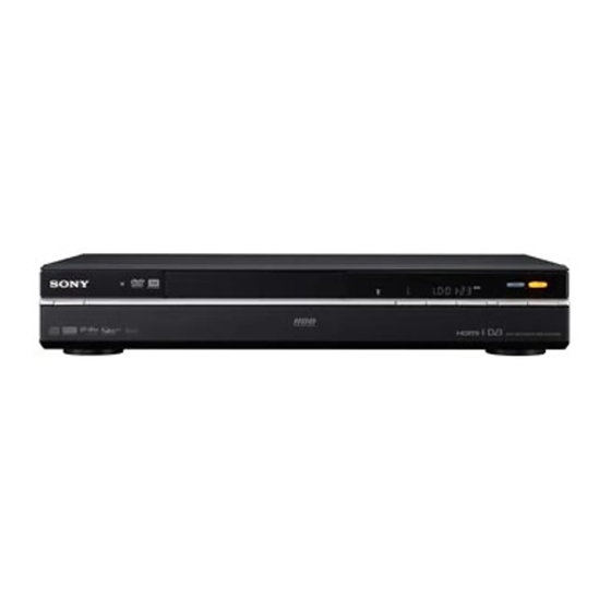
Photo: RDR-HXD1095
RMT-D251P
SPECIFICATIONS
Inputs and outputs
LINE 2 OUT
(AUDIO): Phono jack/2 Vrms/10 kilohms
(VIDEO): Phono jack/1.0 Vp-p
(S VIDEO): 4-pin mini DIN/Y: 1.0 Vp-p,
C: 0.3 Vp-p (PAL)
LINE 2 IN
(AUDIO): Phono jack/2 Vrms/more than
22 kilohms
(VIDEO): Phono jack/1.0 Vp-p
(S VIDEO): 4-pin mini DIN/Y: 1.0 Vp-p,
C: 0.3 Vp-p (PAL)
LINE 3 – TV: 21-pin
CVBS OUT
S-Video/RGB OUT (upstream)
LINE 1/DECODER: 21-pin
CVBS IN/OUT
S-Video/RGB IN
Decoder
DV IN: 4-pin/i.LINK S100
DIGITAL OUT (COAXIAL): Phono
jack/0.5 Vp-p/75 ohms
COMPONENT VIDEO OUT
(Y, P
/C
, P
/C
):
B
B
R
R
Phono jack/Y: 1.0 Vp-p,
P
/C
: 0.7 Vp-p, P
/C
: 0.7 Vp-p
B
B
R
R
G-LINK*: mini jack
HDMI OUT: HDMI™ Connector
USB:
USB jack Type A (For connecting
digital still camera, Memory card
reader, USB memory and HDD
camcorder)
USB jack Type B (For connecting
PictBridge-compatible printers)
Sony Corporation
Home Electronics Network Company
RMT-D251O/D251P
AEP Model
UK Model
RDR-HXD790/HXD795/
HXD890/HXD895/
HXD990/HXD995/
HXD1090/HXD1095
Australian Model
RDR-HXD890/HXD990
Conditional access module (RDR-
HXD795/HXD895/HXD995/
HXD1095 only): CAM (Conditional
Access Module) slot
General
Power requirements: 220-240 V AC,
50/60 Hz
Power consumption: 43 W
RDR-HXD790/HXD890/HXD990/
HXD1090: 47W (AEP, UK)
RDR-HXD890/HXD990: 47W (AUS)
RDR-HXD795/HXD895/HXD995/
HXD1095: 49W (AEP,UK)
AEP, UK Model: With CI card slot
Dimensions (approx.):
430 x 76.5 x 288 mm (width/height/
depth) incl. projecting parts
Hard disk drive capacity:
RDR-HXD790/HXD795: 120 GB
RDR-HXD890/HXD895: 160 GB
RDR-HXD990/HXD995: 250 GB
RDR-HXD1090/HXD1095: 500 GB
Mass (approx.): 4.7 kg
Operating temperature: 5ºC to 35ºC
Operating humidity: 25% to 80%
Supplied accessories:
Mains lead (1)
Aerial cable (1)*
Remote commander (remote) (1)
Set top box controller (1)
R6 (size AA) batteries (2)
*
Two aerial cable are supplied for some
models.
Specifications and design are subject to
change without notice.
DVD RECORDER
Published by Quality Assurance Dept.
2008F1600-1
©2008.06
Advertisement
Table of Contents

Related Manuals for Sony RDR-HXD790


Summary of Contents for Sony RDR-HXD790
- Page 1 B to Q LINE 1/DECODER: 21-pin Hard disk drive capacity: HYPER: S21 to S41 CVBS IN/OUT RDR-HXD790/HXD795: 120 GB S-Video/RGB IN RDR-HXD890/HXD895: 160 GB The above channel coverage merely ensures Decoder RDR-HXD990/HXD995: 250 GB the channel reception within these ranges. It...
-
Page 2: Table Of Contents
TABLE OF CONTENTS SERVICE NOTE • RD-066 (1/7) (POWER BLOCK) DISK REMOVAL PROCEDURE IF THE TRAY SCHEMATIC DIAGRAM ···························· 4-25 CANNOT BE EJECTED (FORCED EJECTION) ········· 1-1 • RD-066 (2/7) (EMMA BLOCK) BOARD CONNECTION, SERVICE REMOTE SCHEMATIC DIAGRAM ···························· 4-27 CONTROLLER ·······························································... - Page 3 ADJUSTMENTS 7-1. Video System Adjustment ··············································· 7-1 REPAIR PARTS LIST 8-1. EXPLODED VIEWS 8-1-1. OVERALL SECTION····················································· 8-1 8-1-2. CHASSIS SECTION ······················································· 8-2 8-2. ELECTRICAL PARTS LIST ·········································· 8-3 — 4 —...
-
Page 4: Service Note
RDR-HXD790/HXD795/HXD890/HXD895/HXD990/HXD995/HXD1090/HXD1095 SECTION 1 SERVICE NOTE 1. DISK REMOVAL PROCEDURE IF THE TRAY CANNOT BE EJECTED (FORCED EJECTION) Remove the upper case. Insert the stiff wire in the hole and eject the tray. Hole 1 The stiff wire 2 Open the tray NOTES DURING THE FORCED EJECTION If the forced ejection is executed while a blank disc media (DVD±RW, ±R) exists on the tray... -
Page 5: Model Name Setting Method When Engine
* Upon completion of the model name setting, be sure to press both “ENTER” and “3” simultaneously on the service remote controll er without fail. It sets the remote control code “3”. Table1 Correspondence table between tentative model name and final product name Tentative model name Model name AEP1 AEP2 AEP3 RDR-HXD790 MRX-1740/EC1 — MRX-1740/EC1 MRX-1740/CEK — RDR-HXD795 —... -
Page 6: How To Diagnose Hdd Failure
Failure to physically Replace the SATA cable or Please consult your identify the HDD (no Blank space power cable. nearest Sony dealer. connection, defective Replace the HDD. Note that contents on HDD, interface error). Replace the FE or part in the the HDD may be SATA/ATA communication. -
Page 7: Display [E01] On Fld With Unrecognized Hdd
4-3. Display [E01] on FLD with unrecognized HDD Is the HDD free from abnormal noises? Refer to “Note”. Is not “#” displayed? Unauthorized HDD Replace the HDD Note: Write down the HDD information on the HDD return sheet before replacing the HDD. Note the information on pages 6-6, 6-7, 6-9, and 6-10 of Chapter 6, “SERVICE MODE”. -
Page 8: Display [E02] On Fld
4-4. Display [E02] on FLD Note: When E02 is displayed, the user data has already broken due to system DATA Error. Is the HDD free from Refer to “Note”. Replace the HDD abnormal noises? Factory check Final check Note: Performing “Final Check” will not erase the HDD data. Has the Final check ended Refer to “Note”. -
Page 9: Factory Check
4-6. Factory Check Pull out and then reconnect the AC cable. Press “ESC” key followed by “P.RUN” key to start Formatting. When “B COMPLETE” appears, the Factory Check is complete. Press “Power” button. The unit starts normally. When “Factory Check” has finished completely without error , reset “Recording Error History” and “A TA/ATAPI History Error” with the Clear key. - Page 10 Diagnosis results • Without an error: “. . . Completed” is displayed. Then, proceed to the Extended Self-Test. • With an error: “. . . Error” is displayed. Look at the number in Test Result. If the place value for tens is 1 or 2, execute the Self-Test again. If it is from 3 to 7, the HDD must be replaced.
-
Page 11: Notice Of Traverse Mecha (Tm) Exchange1-8
5. Notice of traverse mecha (TM) exchange. Distinguish the symptom according to the following procedure Defective set Electrical symptoms Mechanical symptoms READ WRITE Not read the disc Sound and picture interrupt Can’t initialize the disc. On playing back DVD and CD. Noise appears on recording After completed the recording, Then disc was scratched... -
Page 12: Disassembly
RDR-HXD790/HXD795/HXD890/HXD895/HXD990/HXD995/HXD1090/HXD1095 SECTION 2 DISASSEMBLY NOTE: The following flow chart shows the disassembly procedure. Upper case (Page 2-1) Tray cover assembly HDD unit (Page 2-2) (Page 2-7) Front panel block (Page 2-3) FR-291 board, DVD unit FL-184 board (Page 2-5) (Page 2-4) -
Page 13: Upper Case
NOTE: Follow the disassembly procedure in the numerical order given. 2-1. UPPER CASE 4 Upper case 2 Tapping screw 3 Three screws (special front point screw) 1 Tapping screw 2-2. TRAY COVER ASSEMBLY Hole 3 Two claws 1 The stiff wire 2 Open the tray 4 Tray cover assembly... -
Page 14: Front Panel Block
2-3. FRONT PANEL BLOCK 1 Three claws 2 Four claws 3 Front panel block 2-4. FR-291 BOARD, FL-184 BOARD 2 RU-001 harness (10p) (CN102) 3 RV-003 harness (6p) (CN101) 5 FL-184 board 4 Two screws (CN201) (+BV3) (CN106) 7 FAR-008 flexible flat cable 1 FLR-010 or FLR-012 flexible (24core) (CN202) 6 Three screws... -
Page 15: Dvd Unit
2-5. DVD UNIT 3 PH-080 harness (4p) (CN203) 5 RH-059 harness 7 Screw (+P3) (7p) (CN5604) 4 PR-078 harness (13p) (CN201) 8 Two screws (+BV3) 9 Two screws (+P3 × 4) 0 Screw (+BV3) qa Screw (+P3 × 4) qs Five screws (+BV3) qd Screw (+P3 ×... -
Page 16: Dc Fan
2-6. DC FAN 3 Two screws (+BV3) 4 DC fan 1 The wire pin that holds the harness is set up. Air flow 2 Fan harness (2p) (CN203) 2-7. HDD UNIT 5 RH-059 harness (7pin) (power) 3 Screw (+BV3) 4 PH-080 harness and wire clamp (4pin) (data) 1 Two screws (+BV3) -
Page 17: Bracket, Dt
2-8. BRACKET, DT 5 Two screws 6 BRACKET, DT(L) (+BV3) 2 Two screws (+BV3) 3 BRACKET, DT(R) 4 Screw (+BV3) 1 Screw (+BV3) 2-9. AV-133 BOARD 6 FAD-010 flexible flat cable (19core) (CN302) 5 FRA-006 flexible flat cable (40core) (CN101) 7 Three screws (+BV3) 8 AV-133 board... -
Page 18: Switching Regulator
2-10.DT-124 BOARD 2 FVR-001 Flexible flat cable (28core) (CN102) 4 Six screws 1 PD-142 harness (+BV3) (12p) (CN202) 5 DT-124 board 3 FAD-010 flexible flat cable (19core) (CN103) 2-11. SWITCHING REGULATOR 1 PD-142 harness (12p) (CN202) 2 Three screws (+BV3) 5 Switching regulator 3 Two board holders 4 Spacer... -
Page 19: Circuit Boards Location
2-12.CIRCUIT BOARDS LOCATION RD-066 board POWER, EMMA, VIDEO/AUDIO, MEMORY, SATA/IDE IF, HDMI/DV/USB, DVD DRIVE Switching Regulator FL-184 board DV, USB, REMOCON RECEIVER AV-133 board IT CONTROLLER, IR, POWER, FAN CONT, FR-291 board VIDEO/AUDIO, EURO, TUNER FL DRIVER, LINE 2 IN FUNCTION SW DT-124 board DIGITAL TUNER, EMMA,... -
Page 20: Block Diagrams
RDR-HXD790/HXD795/HXD890/HXD895/HXD990/HXD995/HXD1090/HXD1095 SECTION 3 BLOCK DIAGRAMS 3-1. OVERALL BLOCK DIAGRAM CN201 RDR-HXD795/HXD895/HXD995/HXD1095 model only X100 DT-124 BOARD 27MHz IC101 256M Bit IC104 DDR SDRAM 27MHz IC3004 IC3009 IC3002 IC3001 IC205 VCXO IC3005 IC3010 IC3003 32M Bit BUFFER FLASH ROM P-CONT BUFFER... -
Page 21: Block Diagram
RDR-HXD790/HXD795/HXD890/HXD895/HXD990/HXD995/HXD1090/HXD1095 3-2. AV-133 BLOCK DIAGRAM AV-133 BOARD Q509 BTOMAIN DTTY BUFFER FROM DT-124 BOARD Q510 (CN103(2/2)) GTOMAIN DTTC (SEE PAGE 3-6) BUFFER CN302 U601 Q511 Q408 (1/2) RTOMAIN C/R IN UHF/VHF BUFFER BUFFER Q411 TUNER Q601 (3/5) D420 IC401 RCSEL1... - Page 22 IC106 X300 20MHz U301 EMMA XCOFDM_RESET PPORT20 DIGITAL I2C SCA DTBR SDA0 TUNER AERIAL I2C SDL DTBR SCL0 IC313 RDR-HXD790/HXD890/HXD990/HXD1090 model only IF OUT1 OFDM TS1 DATA 0-7 IC104 DEMODULATOR IF OUT2 CLK27IN X100 27MHz TS1_MCLK 27MHz VCXO PWMOUT TS1_MVAL...
-
Page 23: Block Diagram
RDR-HXD790/HXD795/HXD890/HXD895/HXD990/HXD995/HXD1090/HXD1095 3-4. RD-066 BLOCK DIAGRAM RD-066 BOARD 24,26,28,30, V14,U11,U12,W15, IC1001 (2/7,4/7 to 7/7 ) AT0D00 32,34,36,38, V11,T12,P13,R15, OPTICAL AT0DATA0-15 37,35,33,31, R13,V10,P15,U13, 17,15,13,11, PICK-UP AT0D015 29,27,25,23 9,7,5,3, AV ENC/DEC R14,U15,W13,T14 BLOCK AT1DATA0-15 DD0-15 4,6,8,10, AT0DA0 12,14,16,18 W2EN+. W2EN- CN4701 PKPULSEP1P, AT0ADR0-2... -
Page 24: Block Diagram
RDR-HXD790/HXD795/HXD890/HXD895/HXD990/HXD995/HXD1090/HXD1095 3-5. FR-291, FL-184 BLOCK DIAGRAM FR-291 BOARD Q206 LED DRIVE D214 LED2 Q205 D212 LED3 LED DRIVE IC201 SEG1 FL DRIVER SEG16 SG16 GRD1 FLDATA FLCLK GRD12 FLSTB GR12 ND201 FLUORESCENT T201 DISPLAY Q203,204 DC/AC CONVERTER TRASFORMER V+12RIE D208-211... -
Page 25: Power Block Diagram
RDR-HXD790/HXD795/HXD890/HXD895/HXD990/HXD995/HXD1090/HXD1095 3-6. POWER BLOCK DIAGRAM SW+12V(H) SWITCHING REGULATOR SW+5V(H) T101 CN203 SWITCHING SW+1.5V(T) TRANSFORMER UNIT SPINDLE D401 11,12 P401 MOTOR OPTICAL PICK-UP BLOCK EV+12V(T) EV+12V FU101 D101-104 P201 EV+5.8V(T) Q401,402 VA5V VD3V T3.15A/250V SW+12V SW+3.3V(T) 6,16 AC IN P_ON/OFF D402... -
Page 26: Schematic Diagrams And Printed Wiring Boards
RDR-HXD790/HXD795/HXD890/HXD895/HXD990/HXD995/HXD1090/HXD1095 SECTION 4 SCHEMATIC DIAGRAMS AND PRINTED WIRING BOARDS 4-1. FRAME SCHEMATIC DIAGRAM CN201 13P EV+5.8V(M ) PH-080 SW+1.5V(M ) SW+1.5V(M ) HARNESS DVD-UNIT GND D SW+3.3V(M ) SW+3.3V(M ) HDD UNIT SW+12V CN101 50P GND(J) SW+5V(W ) GND(W) SW+12V(W) -
Page 27: Schematic Diagrams
RDR-HXD790/HXD795/HXD890/HXD895/HXD990/HXD995/HXD1090/HXD1095 4-2. SCHEMATIC DIAGRAMS AV-133 THIS NOTE IS COMMON FOR SCHEMATIC DIAGRAMS BOARD (In addition to this, the necessary note is printed in each block) IC101 (X101) IC101 (X102) IC601 (X601) (For printed wiring boards) • Readings are taken with a color-bar signals on D VD reference •... - Page 28 RDR-HXD790/HXD795/HXD890/HXD895/HXD990/HXD995/HXD1090/HXD1095 For Schematic Diagram • Refer to page 4-4 for waveforms. • Refer to page 4-43 for printed wiring board. Q103 R147 UMD2N-TR AV-133 BOARD(1/5) D106 1SS355TE-17 IT CONTROLLER, IR Note : The components identified by mark 0 or dotted...
-
Page 29: 2/5) (Power/Fan Cont.)
RDR-HXD790/HXD795/HXD890/HXD895/HXD990/HXD995/HXD1090/HXD1095 For Schematic Diagram • Refer to page 4-43 for printed wiring board. AV-133 BOARD(2/5) POWER/FAN CONT. SIGNAL PATH -REF.NO.: 10,000 SERIES- VIDEO SIGNAL AUDI O CHROMA Y/CHROMA SIGNAL C303 V+5VV D301 (V+5VI) UDZSNTPE-1715B V+12R1 C301 JL330 TO (4/5) JL319... -
Page 30: 3/5) (Video/Audio)
RDR-HXD790/HXD795/HXD890/HXD895/HXD990/HXD995/HXD1090/HXD1095 For Schematic Diagram • Refer to page 4-4 for waveforms. • Refer to page 4-43 for printed wiring board. AV-133 BOARD(3/5) VIDEO/AUDIO -REF.NO.: 10,000 SERIES- L_OUT L_OUT R_OUT R_OUT 2VIN 2VIN C2IN C2IN Q410 Q411 Y2IN Y2IN 2SC4154TP-1EF UMD2N-TR... - Page 31 RDR-HXD790/HXD795/HXD890/HXD895/HXD990/HXD995/HXD1090/HXD1095 For Schematic Diagram • Refer to page 4-4 for waveforms. • Abbreviation • Refer to page 4-43 for printed wiring board. AUS : Australian model AV-133 BOARD(4/5) EURO -REF.NO.: 10,000 SERIES- V+12R1 (V+5VI) V+5VV TO (2/5) R569 R566 C551...
- Page 32 RDR-HXD790/HXD795/HXD890/HXD895/HXD990/HXD995/HXD1090/HXD1095 For Schematic Diagram • Refer to page 4-4 for waveforms. • Refer to page 4-43 for printed wiring board. AERIAL AV-133 BOARD(5/5) TUNER SIGNAL PATH U601 -REF.NO.: 10,000 SERIES- VIDEO SIGNAL AUDI O CHROMA Y/CHROMA SIGNAL R635 R638 L601...
- Page 33 RDR-HXD790/HXD795/HXD890/HXD895/HXD990/HXD995/HXD1090/HXD1095 For Schematic Diagram • Refer to page 4-3 for waveforms. • Refer to page 4-47 for printed wiring board. DT-124 BOARD(1/3) SIGNAL PATH EMMA VIDEO SIGNAL -REF.NO.: 40,000 SERIES- AUDI O CHROMA Y/CHROMA SIGNAL FAN- DT_TUON TPS_CI_CTRL ANT5V_SW XCI_VCC_5V...
- Page 34 RDR-HXD790/HXD795/HXD890/HXD895/HXD990/HXD995/HXD1090/HXD1095 For Schematic Diagram • Refer to page 4-47 for printed wiring board. *CN201 DT-124 BOARD(2/3) MDATA3 MDATA4 -REF.NO.: 40,000 SERIES- MDATA5 MDATA6 IC3011 R3121 R3119 MDATA7 4.7k IC3015 MDC1_ENABLE GATE C3022 R3118 MADRS10 GATE IC3011 R3122 Q205 2.2k 2.2k...
-
Page 35: 3/3) (Digital Tuner)
RDR-HXD790/HXD795/HXD890/HXD895/HXD990/HXD995/HXD1090/HXD1095 For Schematic Diagram • Refer to page 4-3 for waveforms. • Refer to page 4-47 for printed wiring board. SIGNAL PATH DT-124 BOARD(3/3) DIGITAL AERIAL DIGITAL TUNER VIDEO SIGNAL U301 DTT TUNER AUDI O -REF.NO.: 40,000 SERIES- CHROMA Y/CHROMA... -
Page 36: Fl Driver, Line 2 In, Function Sw)
RDR-HXD790/HXD795/HXD890/HXD895/HXD990/HXD995/HXD1090/HXD1095 For Schematic Diagram • Refer to page 4-3 for waveforms. • Refer to page 4-41 for printed wiring board. ND201 FLUORESCENT TUBE DISPLAY FR-291 BOARD FL DRIVER, LINE 2 IN, FUNCTION SW -REF.NO.: 30,000 SERIES- 10 11 12 23 24... -
Page 37: Dv, Usb, Remocon Receiver, Power Sw
RDR-HXD790/HXD795/HXD890/HXD895/HXD990/HXD995/HXD1090/HXD1095 For Schematic Diagram • Refer to page 4-55 for printed wiring board. FL-184 BOARD DV,USB,REMOCON RECEIVER,POWER,SW -REF.NO.: 30,000 SERIES- CN101 JL101 TPB N FL101 JL102 TPBP RD-066 JL103 BOARD(6/7) CN5101 THROUGH THE CN103 JL104 TPB- RV-003 HARNESS TPAP JL105... -
Page 38: 1/7) (Power Block)
RDR-HXD790/HXD795/HXD890/HXD895/HXD990/HXD995/HXD1090/HXD1095 For Schematic Diagram • Refer to page 4-51 for printed wiring board. RD-066 BOARD(1/7) POWER BLOCK V+1R0 V+1R0 TP4502 TP4503 -REF.NO.: 20,000 SERIES- V+1R5_IN V+1R5_IN EV+5.8V V+3V V+2R5 V+2R5 IC4561 TP4608 NJM2878F3-05(TE2) IC4561 V+3A C4507 C4501 C4535 V+3A 1000p 6.3V... -
Page 39: 2/7) (Emma Block)
RDR-HXD790/HXD795/HXD890/HXD895/HXD990/HXD995/HXD1090/HXD1095 For Schematic Diagram • Refer to page 4-3 for waveforms. • Refer to page 4-51 for printed wiring board. RD-066 BOARD(2/7) L1831 R1312 R1315 C1812 0.5% C1811 R1812 C1045 C1044 1608 1608 TP1202 EMMA BLOCK SIGNAL PATH 6.3V Q1811... -
Page 40: 3/7) (Video/Audio Block)
RDR-HXD790/HXD795/HXD890/HXD895/HXD990/HXD995/HXD1090/HXD1095 For Schematic Diagram • Refer to page 4-51 for printed wiring board. RD-066 BOARD(3/7) VIDEO/AUDIO BLOCK -REF.NO.: 20,000 SERIES- R3234 TU_DSDA TU_DSDA DACCLKO TU_CEC Q2501 - Q2505 TU_CEC IC3201 VIDEO BUFFER TU_DSCL PCM1742KE TU_DSCL R3209 R2501 R3201 R3233 IC3201... -
Page 41: 4/7) (Memory Block)
RDR-HXD790/HXD795/HXD890/HXD895/HXD990/HXD995/HXD1090/HXD1095 For Schematic Diagram • Refer to page 4-51 for printed wiring board. RD-066 BOARD(4/7) MEMORY BLOCK IC1001 (2/5) -REF.NO.: 20,000 SERIES- AV ENC/DEC IC1001 MC10050F1-505-LU1-A IC1201 C1215 C1235 IC201 DDR SDRAM DADRS0 2012 IC1201 C1204 DADD00 FLASH ROM DADRS1... -
Page 42: 5/7) (Sata/Ide If)
RDR-HXD790/HXD795/HXD890/HXD895/HXD990/HXD995/HXD1090/HXD1095 For Schematic Diagram • Refer to page 4-3 for waveforms. • Refer to page 4-51 for printed wiring board. RD-066 BOARD(5/7) SATA/IDE IF IC1001 ( 3/5) -REF.NO.: 20,000 SERIES- AV ENC/DEC IC1001 MC10050F1-505-LU1-A C3802 C3801 6.3V 6.3V R3808 AT1DATA0... -
Page 43: 6/7) (Hdmi/Dv/Usb Block)
RDR-HXD790/HXD795/HXD890/HXD895/HXD990/HXD995/HXD1090/HXD1095 For Schematic Diagram • Refer to page 4-3 for waveforms. • Refer to page 4-51 for printed wiring board. RD-066 BOARD(6/7) HDMI/DV/USB BLOCK -REF.NO.: 20,000 SERIES- IC1001 (4/5) AV ENC/DEC R5215 R5201 IC5203 USB_DN0 IC1001 MC10050F1-505-LU1-A R5825 AND GATE... -
Page 44: 7/7) (Dvd Drive)
RDR-HXD790/HXD795/HXD890/HXD895/HXD990/HXD995/HXD1090/HXD1095 For Schematic Diagram • Refer to page 4-51 for printed wiring board. CN101 TP171 TP173 RD-066 BOARD(7/7) TP175 TP177 DVD DRIVE TP187 SCLK SCLK -REF.NO.: 20,000 SERIES- TP183 SDIO R313 LCDS TP184 R115 TP182 TP181 RESET XRESET TP179 VD3V... -
Page 45: Switching Regulator (Srv-2100Ek)
RDR-HXD790/HXD795/HXD890/HXD895/HXD990/HXD995/HXD1090/HXD1095 SWITCHING REGULATOR (SRV-2100EK) CN202 P401 P-CONT D401 1.6A/32V SF5LC20U SW +3.3V T101 Q401 C407 MPA2733GR SWITCHING TRANSFORMER D101-104 1000p 12V REG SW +3.3V RECT C402 TO DT-124 P201 470u C405 R401 2A/32V BOARD(3/3) R115 0.1u 100k D103 C111 D101... -
Page 46: Switching Regulator Srv-2057Ek
RDR-HXD790/HXD795/HXD890/HXD895/HXD990/HXD995/HXD1090/HXD1095 SWITCHING REGULATOR C134 CN202 220p (SRV-2057EK) (Australian model) 250V L105 P401 P-CONT D401 1.6A/32V SF5LC20U SW +3.3V T101 Q401 C407 uPA2733GR SWITCHING TRANSFORMER D101-104 1000p 12V REG TO DT-124 SW +3.3V RECT C402 P201 BOARD(3/3) 470u C405 R401 2A/32V... -
Page 47: Printed Wiring Boards
RDR-HXD790/HXD795/HXD890/HXD895/HXD990/HXD995/HXD1090/HXD1095 4-3. PRINTED WIRING BOARDS FR-291 BOARD(SIDE A) • : Uses unleaded solder. D212 D214 ND201 C201 T201 L201 S208 S210 Q201 Q202 A201 R251 R250 C216 OPEN/CLOSE PLAY STOP S202 S205 S204 S207 S203 S201 S209 S206 J201 REC STOP... -
Page 48: Controller, Ir, Power/Fan Cont, Video/Audio, Euro, Tuner
RDR-HXD790/HXD795/HXD890/HXD895/HXD990/HXD995/HXD1090/HXD1095 AV-133 BOARD(SIDE A) • : Uses unleaded solder. AV-133 BOARD (SIDE A) CN101 CN105 CN302 C639 C311 C638 TUNER KN101 C312 Q303 D101 C618 C617 C642 D102 R625 C619 JL656 JL648 Q304 C118 D103 U601 JL661 JL316 JL647 D104... - Page 49 RDR-HXD790/HXD795/HXD890/HXD895/HXD990/HXD995/HXD1090/HXD1095 AV-133 BOARD(SIDE B) • : Uses unleaded solder. AV-133 BOARD (SIDE B) D201 D301 D302 D303 D304 C621 R609 C309 D409 R630 D410 C615 Q606 C616 D413 C614 D414 Q601 R304 L601 D415 C305 D416 Q302 D418 L606 R607...
-
Page 50: Emma2Ll, Ci, Digital Tuner
RDR-HXD790/HXD795/HXD890/HXD895/HXD990/HXD995/HXD1090/HXD1095 DT-124 BOARD(SIDE A) • : Uses unleaded solder. DT-124 BOARD (SIDE A) CN102 CN103 R529 CN103 R527 R345 C801 CN201 R528 Q801 R802 CN202 TUNER Q802 R801 Q804 R530 CN203 R814 C807 R807 R803 C211 R813 R808 R810 TP826... - Page 51 RDR-HXD790/HXD795/HXD890/HXD895/HXD990/HXD995/HXD1090/HXD1095 DT-124 BOARD(SIDE B) • : Uses unleaded solder. DT-124 BOARD (SIDE B) D302 D303 R628 R306 C339 IC207 R347 IC304 IC306 IC307 IC309 R3123 C221 R3124 R273 IC312 Q202 C3013 Q203 TP857 C222 IC3001 R363 R272 C382 IC3015 R275...
- Page 52 RDR-HXD790/HXD795/HXD890/HXD895/HXD990/HXD995/HXD1090/HXD1095 RD-066 BOARD(SIDE A) • : Uses unleaded solder. RD-066 BOARD (SIDE A) CN1401 CN1402 CN201 CN2301 CN3802 CN4501 CN4701 CN5604 D1401 D3201 TP3801 C4555 D4521 TP3803 TP3802 D4552 TP3804 TP3805 IC4552 TP3806 R4558 TP3807 IC1001 TP3808 C4556 TP3809 TP3810...
- Page 53 RDR-HXD790/HXD795/HXD890/HXD895/HXD990/HXD995/HXD1090/HXD1095 RD-066 BOARD(SIDE B) • : Uses unleaded solder. RD-066 BOARD (SIDE B) TP611 TP4604 TP4605 CN101 TP605 CN501 R604 R602 TP610 TP196 CN101 CN601 TP607 CN502 TP612 R603 R601 TP191 CN5101 TP171 C503 C508 TP4606 CN501 TP507 TP182 CN5201...
-
Page 54: Dv, Usb, Remocon Receiver, Power Sw
RDR-HXD790/HXD795/HXD890/HXD895/HXD990/HXD995/HXD1090/HXD1095 FL-184 BOARD(SIDE A) • : Uses unleaded solder. FL-184 BOARD (SIDE A) CN101 CN102 CN103 CN104 CN105 IC101 C111 CN106 IC101 LP101 1-875-775- CN101 CN102 VDR102 (POWER) VDR104 S102 S101 CN103 CN105 CN104 TOUCH DUB DV IN B TYPE... -
Page 55: Ic Pin Function Description
RDR-HXD790/HXD795/HXD890/HXD895/HXD990/HXD995/HXD1090/HXD1095 SECTION 5 IC PIN FUNCTION DESCRIPTION 5-1. IT CONTROL IC (IC101:LC87F06J2A-F59P6-E (AV-133 BOARD)) Pin No. Pin Name Function — Not used — Not used — Not used — Fixed at “H” ACDET Input of IC’s VDD detect signal HSM_TO_T... - Page 56 Pin No. Pin Name Function FLCLK Output of clock signal for FLD driver RFTHRU Output of tuner power supply control signal — Not used FANCTL Output of fan direction speed switching signal VDD2 — Power supply input — Analog GND P_CONT2 Output of system power supply control signal [2] MUTECTL...
-
Page 57: Av Encoder/Decoder Ic
5-2. AV ENCODER/DECODER IC (IC1001:MC10050F1-505-LU1-A (RD-066 BOARD)) Pin No. Pin Name Function DGND — Digital GND DRASB Output of RAS signal DBA1 Output of bank address [1] DADD01 Output of DDRSDRAM address [1] DDQM1 Output of data mask [1] DQ13 Input/output of DDRSDRAM data [13] DQ11 Input/output of DDRSDRAM data [11]... - Page 58 Pin No. Pin Name Function PDIAGB — Not used AC19 MONI3 — Not used AC20 SP1EN — Fixed at GND AC21 SP1DAT2 — Fixed at GND AC22 VIOD7 Input/output of digital video data [7] AC23 SP1DAT7 — Fixed at GND AC24 VIOD6 Input/output of digital video data [6]...
- Page 59 Pin No. Pin Name Function AE23 SP1DAT4 — Fixed at GND AE24 VIOD1 Input/output of digital video data [1] Input/output of clock 16.9344MHz Output of buffer memory interface write enable Output of buffer memory interface address bus [2] RSAB Output of buffer memory interface row address strove control (PB2) Output of buffer memory interface bank address [MA11] Output of DDO...
- Page 60 Pin No. Pin Name Function WRPULSEP Output of write pulse (laser driver control signal for write) HFONP Output of laser driver high frequency superposition control signal Input of RXDA2 signal Output of RCDT signal Input of sub beam signal H1 G1/FOP Input of sub beam signal G1 AH10...
- Page 61 Pin No. Pin Name Function DDQM3 Output of data mask [3] Not open to public Input of monitor sense Not open to public Output of data [11] Not open to public Output of data [8] Not open to public Output of data [5] Not open to public Output of data [2] Not open to public...
- Page 62 Pin No. Pin Name Function CTL1 Input/output of PHY/link control [1] for PHY SCLK Input of link control clock for PHY Output of link power status SCL1 Input/output of serial clock DCD0B Input of data carrier detect from AG2 pin Output of digital audio AOLRCK Output of audio L/R clock...
- Page 63 Pin No. Pin Name Function AILRCK0 Input of audio L/R clock [0] IR_IN Input of IR receiver JTDI Input of EJTAG data VRTR — Fixed at “L” Input of AD converter for analog video signal blue VRBR — Fixed at “L” DQ16 Input/output of DDRSDRAM data [16] DQ17...
- Page 64 Pin No. Pin Name Function DVDD33(3.3V) — Power supply input DVDD33(3.3V) — Power supply input DGNDR — GND (for RF) HLCO Output of H lock clock for video decoder HC_VDD3 — Power supply input (3.0V for V DEC) FC_VDD3 — Power supply input (3.0V for V DEC) FSCO Output of FSC for video decoder...
- Page 65 Pin No. Pin Name Function DVDD10(1.0V) — Power supply input DVDD33(3.3V) — Power supply input AVDD33R — Power supply input (3.0V for RF) RADD24 Input of ROM/GIO address [24] RDATA14 Input/output of ROM/GIO data [14] RADD18 Output of ROM/GIO address [18] RDATA13 Input/output of ROM/GIO data [13] RDATA07...
- Page 66 Pin No. Pin Name Function AT0D05 Output of data [05] for IDE I/F AT0IORDY Output of IORDY signal for IDE I/F AT0D15 Output of data [15] for IDE I/F AT0DMARQ Output of DMARQ signal for IDE I/F GCSB3 Output of GIO chip select [3] GCSB1 —...
- Page 67 Pin No. Pin Name Function AT0CS1B Output of chip select signal [1] for IDE I/F AT0CS0B Output of chip select signal [0] for IDE I/F AT0D14 Output of data [14] for IDE I/F AT0DA0 Output of address [0] for IDE I/F AT0D03 Output of data [03] for IDE I/F SP1REQB...
-
Page 68: Service Mode
RDR-HXD790/HXD795/HXD890/HXD895/HXD990/HXD995/HXD1090/HXD1095 SECTION 6 SERVICE MODE Prepairing for Service tool • Color monitor • Service remote controller (Part code: J-6090-203-A) OPEN/CLOSE button SPEED SPEED button Number button TV/LDP button TV/LDP +10 button STEREO button CLEAR STEREO CLEAR button FRM/TIM button FRM/TIM CHAP... -
Page 69: Service Mode Map
6-1. SERVICE MODE MAP [Operation] [Mode / Name] < First screen > DISP Version info, etc 3 times < First screen subscreen 3 > DIG/ANA HDD information < First screen subscreen 4 > DIG/ANA OSD Filter setting DISP DIG/ANA 2 times <... -
Page 70: Diagnostic Mode
6-2. Diagnostic Mode 6-2-1. Model Setting Turn of the main power ON. On the screen after exiting all menu screen’ s, press the following buttons “ESC” k “CHAP” k “1” on the service remote controller. Turn of the main power OFF. Turn of the main power ON. -
Page 71: Service Mode
6-2-2. Service Mode 1) Turn of the main power ON. 2) On the screen after exiting all menu screen’s, press “ESC” on the service remote controller. 3) Press “DISP”. 4) Press “DIG/ANA”. Overview and purposes To be used to check the status of the product and to collect the information for failure diagnosis. The following information to be used for servicing is displayed: [1] First screen : Version, HDD information, etc. -
Page 72: Rf Level Simplified Diagnosis (Subscreen1)
6-2-4. RF Level Simplified Diagnosis (Subscreen1) Turn of the main power ON. On the screen after exiting all menu screens, press “ESC” on the service remote controller. Press “DISP”. Press “DIG/ANA”. * The RF signal status can be obtained from the input frequency - - - - VERSION : 1.** deviation information and the AGC voltage. -
Page 73: Hdd Information For The Hdd Return Sheet (Simplified Measurement Mode)
6-2-5. HDD Information for the HDD return sheet (Simplified measurement mode) HDD Information • How to start/terminate the diagnostic program Use the remote control unit for servicing. How to start: Press the following keys in this order; “ESC”, “CX”, “0”, and “1” keys: (refer to 6-2-15). How to terminate: Press “ESC”... -
Page 74: Cautions For Handling The Hdd
HDD Information (Simplified measurement mode) Turn on the main power. Press “ESC”. Press “DISP”. Press “DIG/ANA” three times. * Checks the HDD power-on time. Info Life Time : --h --m --s [Tips] • How the cumulative HDD-on time data is processed in memory Storage place: FLASH ROM Timing for referring to the cumulative HDD-on time data:... - Page 75 (2) Cautions for handling and examples of dangerous handling for the product that the HDD is mounted on or the HDD repair part [Cautions for handling the product that the HDD is mounted on] • The HDD is always in operation while the unit is turned on. Do NOT to apply shock to the unit. Examples of dangerous handling: while the power is on •...
-
Page 76: Hdd Error Logging
6-2-7. HDD Error Logging Use the following operations to display “Recording Error History”. Press “ESC”, “DSP”, and “4” keys, followed by “DIG/ANA” key three times. Recording Error History Display 07-01-01 00:00:00 HDD Destroy The error display appears in the underlined location. 07-01-01 00:00:00 Mech No Res... -
Page 77: Ata/Atapi History - Err
6-2-8. ATA/ATAPI History - ERR Use the following operations to display “ATA/ATAPI Error History”. Press “ESC” key, followed by “DSP”, “2”, “DIG/ANA”, and “FRM/TIM” key. ATA/ATAPI History - ERR 0223 151843> C8 00013 09387FC4 40FC4051 2B 3C 01 0000 000000 00 00000 00000000 00000000 00 00 00 0000 000000 00 00000 00000000 00000000 00 00 00 0000 000000 00 00000 00000000 00000000 00 00 00 0000 000000 00 00000 00000000 00000000 00 00 00... -
Page 78: Ata/Atapi Debugging Screen Second Screen And Ld Deterioration Judgment (For Writer)
6-2-10. ATA/ATAPI Debugging Screen (Second Screen) and LD Deterioration Judgment (for writer) 1. Writer maintenance information of ATA/ATAPI DEBUG OSD (Subscreen3) Turn of the main power ON. On the screen after exiting all menu screens, press “ESC” on the service remote controller. Press “DISP”. - Page 79 2. LD degration judgment of ATA/ATAPI DEBUG OSD (Subscreen 4) 1) While the User Operation screen is being displayed, press “ESC” on the service remote controller. 2) Press “DISP” on the service remote controller. 3) Press “2” on the service remote controller. 4) Press “DIG/ANA”...
-
Page 80: History Of Vr Recording-Related Errors
6-2-11. History of VR Recording-related Errors Turn of the main power ON. On the screen after exiting all menu screens, press “ESC” on the service remote controller. Press “DISP”. Press “4”. * Used for broadly dividing the poorly-reproducible trouble RunFnc : ---- Ecl : STDBY Rate : 21 VID : 1000 phenomena. - Page 81 Description of VR-recording-related errors Drive System-Related Errors ERROR MESSAGE DESCRIPTION Error Message Contents Bdr Cls NG Close Border failed Bdr Opn NG Open Border failed Abbreviations ECC : 4-byte Code for Error Correction BUF Overflow Overflow of the Stream Buffer UDF : Universal Disc Format CLS Rzon Fail Video mode Close Rzone failure...
- Page 82 Dubbing-Related Errors HDD-Related Errors ERROR MESSAGE DESCRIPTION ERROR MESSAGE DESCRIPTION H2D CP SomeNG Other NG HDD → DVD copy Do nothing Do nothing for demand Mem get NG Video Mode Copy Memory has noe ESFSYS CORUPT easyfsys error ensured ESFSYS INIT easyfsys initializing Strm TransfNG Video Mode Copy Stream Transefer...
- Page 83 Other Errors ERROR MESSAGE DESCRIPTION ERROR MESSAGE DESCRIPTION Abort Cancellation SW PVR Switch to +VR playback process Already open Extension file is already opened SW Vpb mode* Switching to video playback routine is required BK BATT Down Backup RAM Data has been erased SW Vrec mode* Switching to video recording routine BK FSYS Dirty...
-
Page 84: Dv Service Mode
6-2-12. DV Service Mode 1. DV debug Turn of the main power ON. On the screen after exiting all menu screens, press “ESC” on the service remote controller. Press “DISP”. Press “3”. * Used when an error exists in connection with the DV equipment. (DV/1394) Init : NG AV : 02 DV : 01 [Recorder] GUID : 0000000000000000 IRM iPCR : C03F0000... - Page 85 6-18...
-
Page 86: Epg Service Mode
6-2-13. EPG Service Mode 1. Summary screen Turn of the main power ON. On the screen after exiting all menu screens, press “ESC” on the service remote controller. Press “DISP”. Press “7”. 012345678901234567890123456789012345678901234567 * Used when the EPG data cannot be acquired. (EPG EURO) * The detailed screen appears every time when “DIG/ANA”... - Page 87 2. Detail screens 1) Press the “DIG/ANA” key while the Summary screen is being displayed. (Refer to page 6-19) 2) Each time the “DIG/ANA” key is pressed, the Detail screen scrolls maximum six-Detail screens (1 to 6). Each Detail screen of 1 to 6 corresponds to the EPG reception error logs from the top of the Summary screen. 012345678901234567890123456789012345678901234567 (EPG EURO) EPG Data Receive Err Details - 1...
-
Page 88: Aging Mode
6-2-14. Aging Mode 1. Aging for the DVD-RW/DVD-R Turn of the main power ON. Press the “DVD” key to switch to DVD. Load a recordable disc. Select the input function of a recordable source. After disc detection is confirmed, exit all menu screens. Press “ESC”... -
Page 89: Hdd Check Mode
2. Aging for the HDD Caution: Take caution as the all recorded data of HDD is deleted. 1) Turn of the main power ON. 2) Press the “HDD” key to switch to HDD. 3) Press “ESC” on the service remote controller. Press “REP.B”... -
Page 90: Setup Related Menu
6-3. Setup Related Menu 6-3-1. Firmware Downloading In case of any event as described below , be sure to download the software using the Version Upgrade CD Disc by following the So ftware Download Method shown below. When engine (RD board or drive) is replaced, or when the AV board is replaced. When HDD is replaced. -
Page 91: Osd Filter Setting
6-3-3. OSD Filter Setting (Subscreen 4) When the following trouble symptom occurs, correct it by setting the OSD filter as described below. • Characters on the OSD screen flicker depending on the monitor connected. [Entry] 1) Turn of the main power ON. 2) Press “ESC”... -
Page 92: Adjustments
RDR-HXD790/HXD795/HXD890/HXD895/HXD990/HXD995/HXD1090/HXD1095 SECTION 7 ADJUSTMENTS 7-1. Video System Adjustment 2. S-Video Output S-Y Check <Purpose> This check confirms that the S-video Y-signal output has the rated Preparing for Adjustment amplitude. If it adjusted incorrectly, the playback video signal will 1. Equipments not be displayed corrected even when the S-video cable is connected. - Page 93 3. S-Video Output S-C Check <Purpose> This check confirms that the B-Y signal of the component video <Purpose> This check confirms that the S-video output S-C conforms to the conforms to the P AL standard. If this signal level is not correct, PAL standard.
- Page 94 7. Scart Video Output Level Check 9. Scart Video Output S-C Check <Purpose> <Purpose> This check is made to satisfy the P A L signal standard, If it is adjusted This check confirms that the Scart output S-C conforms to the P A L incorrectly, brightness will be too bright or too dark.
- Page 95 11. Scart Video RGB Output G Check <Purpose> This check confirms that G signal of the RGB video conforms to the PAL standard. If this signal level is not correct, color of the video signal will have dif f erent color when the Scart connector output signal is connected to a projector having Scart input.
-
Page 96: Repair Parts List
RDR-HXD790/HXD795/HXD890/HXD895/HXD990/HXD995/HXD1090/HXD1095 SECTION 8 REPAIR PARTS LIST 8-1. EXPLODED VIEWS NOTE: The components identified b y mar k 0 or • -XX, -X mean standardized parts, so they may • Color Indication of Appearance Parts dotted line with mark 0 are critical for safety. -
Page 97: Chassis Section
8-1-2. CHASSIS SECTION supplied supplied supplied supplied supplied supplied U301 not supplied not supplied not supplied supplied U601 not supplied not supplied not supplied not supplied Ref. No. Part No. Description Remarks Ref. No. Part No. Description Remarks 3-077-331-01 +BV3 (3-CR) A-1520-892-A AV-133 (CG) COMPL (AEP, UK) A-1544-210-A HDD (SG-SUPERHAWK-S (250GB)-GA) A-1550-351-A AV-133 (AS) COMPL (AUS) -
Page 98: Electrical Parts List
AV-133 8-2. ELECTRICAL PARTS LIST NOTE: • Due to standardization, replacements in the • RESISTORS When indicating parts by reference number, please include the board name. parts list may be dif ferent from the parts All resistors are in ohms. specified in the diagrams or the components METAL: metal-film resistor used on the set. - Page 99 AV-133 Ref. No. Part No. Description Remarks Ref. No. Part No. Description Remarks C430 1-107-826-11 CERAMIC CHIP 0.1uF C518 1-100-831-91 CERAMIC CHIP 0.001uF C431 1-107-826-11 CERAMIC CHIP 0.1uF C519 1-164-315-11 CERAMIC CHIP 470PF C432 1-165-908-11 CERAMIC CHIP C520 1-100-831-91 CERAMIC CHIP 0.001uF C434 1-107-826-11 CERAMIC CHIP...
- Page 100 AV-133 Ref. No. Part No. Description Remarks Ref. No. Part No. Description Remarks < DIODE > < IC > IC101 6-712-674-01 IC LC87F06J2A-F59P6-E * IC102 D101 8-719-081-97 DIODE MMDL914T1 6-711-071-01 IC BD4846G-TR * IC103 D102 8-719-081-97 DIODE MMDL914T1 6-711-072-01 IC BU4220G-TR * IC104 D103 8-719-081-97 DIODE MMDL914T1...
- Page 101 AV-133 Ref. No. Part No. Description Remarks Ref. No. Part No. Description Remarks Q108 8-729-029-06 TRANSISTOR DTC124EUA-T106 R112 1-216-833-11 METAL CHIP 1/10W Q110 8-729-028-86 TRANSISTOR DTA143EUA-T106 (AEP, UK) R113 1-216-864-11 SHORT CHIP Q111 8-729-620-13 TRANSISTOR 2SC4154TP-1EF R116 1-216-864-11 SHORT CHIP Q112 8-729-620-13 TRANSISTOR 2SC4154TP-1EF...
- Page 102 AV-133 Ref. No. Part No. Description Remarks Ref. No. Part No. Description Remarks R193 1-216-845-11 METAL CHIP 100K 1/10W R431 1-216-857-11 METAL CHIP 1/10W R194 1-216-845-11 METAL CHIP 100K 1/10W R432 1-216-857-11 METAL CHIP 1/10W R195 1-216-845-11 METAL CHIP 100K 1/10W R433 1-216-857-11 METAL CHIP...
- Page 103 AV-133 Ref. No. Part No. Description Remarks Ref. No. Part No. Description Remarks R515 1-216-043-91 RES-CHIP 1/10W R602 1-216-821-11 METAL CHIP 1/10W R516 1-216-822-11 METAL CHIP 1.2K 1/10W R603 1-216-864-11 SHORT CHIP R517 1-216-823-11 METAL CHIP 1.5K 1/10W R605 1-216-833-11 METAL CHIP 1/10W R518 1-216-797-11 METAL CHIP...
- Page 104 DT-124 Ref. No. Part No. Description Remarks Ref. No. Part No. Description Remarks A-1520-890-A DT-124 (AG) BOARD, COMPLETE C194 1-115-156-11 CERAMIC CHIP (HXD790/HXD890: AEP, UK/HXD990: AEP, UK/HXD1090) C209 1-164-156-11 CERAMIC CHIP 0.1uF A-1520-894-A DT-124 (BG) BOARD, COMPLETE (HXD795/HXD895/HXD995/HXD1095) (HXD795/HXD895/HXD995/HXD1095) C210 1-117-681-11 ELECT CHIP 100uF A-1550-357-A DT-124 (AS) BOARD, COMPLETE (AUS)
- Page 105 DT-124 Ref. No. Part No. Description Remarks Ref. No. Part No. Description Remarks C395 1-126-204-11 ELECT CHIP 47uF C3004 1-107-820-11 CERAMIC CHIP 0.1uF C396 1-164-227-11 CERAMIC CHIP 0.022uF (HXD795/HXD895/HXD995/HXD1095) C397 1-162-915-11 CERAMIC CHIP 10PF 0.5PF C3005 1-107-820-11 CERAMIC CHIP 0.1uF C398 1-164-156-11 CERAMIC CHIP 0.1uF...
- Page 106 DT-124 Ref. No. Part No. Description Remarks Ref. No. Part No. Description Remarks < IC > < RESISTOR > IC101 6-705-306-01 IC HYB25DC256160CE-6 R100 1-216-864-11 SHORT CHIP * IC104 6-711-077-01 IC KA5SDKAS01TSN R101 1-216-833-11 METAL CHIP 1/10W IC106 6-711-206-01 IC uPD61111GM-200-UEV-A R104 1-216-833-11 METAL CHIP 1/10W...
- Page 107 DT-124 Ref. No. Part No. Description Remarks Ref. No. Part No. Description Remarks R231 1-216-820-11 METAL CHIP 1/10W R341 1-216-828-11 METAL CHIP 3.9K 1/10W (HXD795/HXD895/HXD995/HXD1095) R342 1-216-828-11 METAL CHIP 3.9K 1/10W R239 1-234-791-21 RES, NETWORK 150X4 (2010) (AEP, UK) R343 1-216-864-11 SHORT CHIP R239 1-200-051-21 RES, NETWORK 150 (1005X4) (AUS)
- Page 108 DT-124 Ref. No. Part No. Description Remarks Ref. No. Part No. Description Remarks R641 1-234-400-21 CONDUCTOR, NETWORK (1005X4) R3011 1-216-864-11 SHORT CHIP R642 1-216-864-11 SHORT CHIP (HXD795/HXD895/HXD995/HXD1095) R660 1-218-847-11 METAL CHIP 0.5% 1/10W R3012 1-218-965-11 RES-CHIP 1/16W R661 1-218-847-11 METAL CHIP 0.5% 1/10W (HXD795/HXD895/HXD995/HXD1095)
- Page 109 DT-124 Ref. No. Part No. Description Remarks Ref. No. Part No. Description Remarks R3052 1-218-935-11 RES-CHIP 1/16W R3085 1-218-937-11 RES-CHIP 1/16W (HXD795/HXD895/HXD995/HXD1095) (HXD795/HXD895/HXD995/HXD1095) R3053 1-218-935-11 RES-CHIP 1/16W R3086 1-218-933-11 RES-CHIP 1/16W (HXD795/HXD895/HXD995/HXD1095) (HXD795/HXD895/HXD995/HXD1095) R3054 1-218-965-11 RES-CHIP 1/16W R3087 1-218-933-11 RES-CHIP 1/16W (HXD795/HXD895/HXD995/HXD1095) (HXD795/HXD895/HXD995/HXD1095)
- Page 110 DT-124 FL-184 FR-291 Ref. No. Part No. Description Remarks Ref. No. Part No. Description Remarks R3122 1-216-825-11 METAL CHIP 2.2K 1/10W < VARISTOR > (HXD795/HXD895/HXD995/HXD1095) R3123 1-218-937-11 RES-CHIP 1/16W VDR102 1-802-071-21 VARISTOR, CHIP (HXD795/HXD895/HXD995/HXD1095) VDR104 1-802-071-21 VARISTOR, CHIP R3124 1-218-937-11 RES-CHIP 1/16W ************************************************************ (HXD795/HXD895/HXD995/HXD1095)
- Page 111 FR-291 RD-66 Ref. No. Part No. Description Remarks Ref. No. Part No. Description Remarks < TRANSISTOR > < TRANSFORMER > * T201 Q201 8-729-052-91 TRANSISTOR 2SD1898T100R 1-445-207-11 TRANSFORMER, DC-DC CONVERTER Q202 8-729-052-91 TRANSISTOR 2SD1898T100R ************************************************************ Q203 8-729-024-43 TRANSISTOR 2SA1365-T112-1EF Q204 8-729-421-19 TRANSISTOR UN2213 Q205...
- Page 112 RD-66 Ref. No. Part No. Description Remarks Ref. No. Part No. Description Remarks C182 1-100-966-91 CERAMIC CHIP 10uF C1032 1-125-777-11 CERAMIC CHIP 0.1uF C187 1-164-943-81 CERAMIC CHIP 0.01uF C1033 1-125-777-11 CERAMIC CHIP 0.1uF C188 1-164-943-81 CERAMIC CHIP 0.01uF C1034 1-125-777-11 CERAMIC CHIP 0.1uF C189 1-164-937-11 CERAMIC CHIP...
- Page 113 RD-66 Ref. No. Part No. Description Remarks Ref. No. Part No. Description Remarks C1401 1-164-943-81 CERAMIC CHIP 0.01uF C3333 1-114-130-11 CERAMIC CHIP 6.3V C1421 1-114-130-11 CERAMIC CHIP 6.3V C3334 1-114-130-11 CERAMIC CHIP 6.3V C1801 1-114-130-11 CERAMIC CHIP 6.3V C3335 1-114-130-11 CERAMIC CHIP 6.3V C1802 1-125-889-11 CERAMIC CHIP...
- Page 114 RD-66 Ref. No. Part No. Description Remarks Ref. No. Part No. Description Remarks C5107 1-114-130-11 CERAMIC CHIP 6.3V C5803 1-114-130-11 CERAMIC CHIP 6.3V C5108 1-114-130-11 CERAMIC CHIP 6.3V C5804 1-164-937-11 CERAMIC CHIP 0.001uF C5110 1-114-130-11 CERAMIC CHIP 6.3V C5805 1-114-130-11 CERAMIC CHIP 6.3V C5111 1-114-130-11 CERAMIC CHIP...
- Page 115 RD-66 Ref. No. Part No. Description Remarks Ref. No. Part No. Description Remarks < COIL > R116 1-218-959-11 RES-CHIP 3.3K 1/16W R117 1-218-939-11 RES-CHIP 1/16W L105 1-469-967-21 INDUCTOR 10uH R119 1-218-990-81 SHORT CHIP L1005 1-412-008-31 INDUCTOR 15uH R124 1-218-990-81 SHORT CHIP L1801 1-412-958-21 INDUCTOR 39uH...
- Page 116 RD-66 Ref. No. Part No. Description Remarks Ref. No. Part No. Description Remarks R319 1-242-963-21 RES, NETWORK 33 (1005X4) R1197 1-218-961-11 RES-CHIP 4.7K 1/16W R320 1-242-963-21 RES, NETWORK 33 (1005X4) R1199 1-218-965-11 RES-CHIP 1/16W R503 1-218-953-11 RES-CHIP 1/16W R1205 1-218-965-11 RES-CHIP 1/16W R504 1-218-953-11 RES-CHIP...
- Page 117 RD-66 Ref. No. Part No. Description Remarks Ref. No. Part No. Description Remarks R1404 1-218-933-11 RES-CHIP 1/16W R3207 1-218-937-11 RES-CHIP 1/16W R1405 1-218-933-11 RES-CHIP 1/16W R3208 1-218-937-11 RES-CHIP 1/16W R1406 1-218-933-11 RES-CHIP 1/16W R3209 1-218-977-11 RES-CHIP 100K 1/16W R1407 1-218-933-11 RES-CHIP 1/16W R3210 1-218-849-11 METAL CHIP...
- Page 118 RD-66 Ref. No. Part No. Description Remarks Ref. No. Part No. Description Remarks R3812 1-242-963-21 RES, NETWORK 33 (1005X4) R4708 1-234-378-21 RES, NETWORK 10K (1005X4) R3813 1-242-963-21 RES, NETWORK 33 (1005X4) R4709 1-234-378-21 RES, NETWORK 10K (1005X4) R3814 1-218-933-11 RES-CHIP 1/16W R4710 1-218-965-11 RES-CHIP...
- Page 119 RD-66 Ref. No. Part No. Description Remarks Ref. No. Part No. Description Remarks R5216 1-218-990-81 SHORT CHIP R5806 1-218-953-11 RES-CHIP 1/16W R5217 1-218-990-81 SHORT CHIP R5807 1-218-962-11 RES-CHIP 5.6K 1/16W R5220 1-218-851-11 METAL CHIP 1.5K 0.5% 1/10W R5808 1-218-961-11 RES-CHIP 4.7K 1/16W R5221...
- Page 120 Ref. No. Part No. Description Remarks Ref. No. Part No. Description Remarks ACCESSORIES *********** 1-480-698-11 REMOTE COMMANDER (RMT-D251P) (AEP, UK) 1-480-700-11 REMOTE COMMANDER (RMT-D251O) (AUS) 1-575-131-82 CORD, POWER (AEP) 1-759-586-41 CONTROLLER, VIDEO (AV MOUSE) (AEP, UK) 1-696-593-11 CORD, CONNECTION (PAL) 1-828-145-11 CORD, CONNECTION (AV) (AUS) 1-827-269-12 CORD, POWER (UK) 1-555-074-52 CORD, POWER (AUS)
- Page 121 2008.06 Official Release — — 2008.11 2008.11 Revised-1 Revised-1 Change of repair parts list (Page 8-2) Change of repair parts list (Page 8-2) Addition of Note (Page 8-2) Addition of IC101(Page 8-5) 2010.01 Revised-2 Addition of Note (Page 1-8) RDR-HXD790/HXD795/HXD890/HXD895/HXD990/HXD995/HXD1090/HXD1095...