Yamaha BBT500H Service Manual
Bass amplifier
Hide thumbs
Also See for BBT500H:
- Handleiding (21 pages) ,
- Preset patch list (1 page) ,
- Owner's manual (21 pages)
Advertisement
Quick Links
GA
011757
20041220-89000
SERVICE MANUAL
(目次)
CONTENTS
(総合仕様)
SPECIFICATIONS
(パネルレイアウト)
PANEL LAYOUT
DISASSEMBLY PROCEDURE
(LSI端子機能表)
LSI PIN DESCRIPTION
(ICブロック図)
IC BLOCK DIAGRAM
(シート基板図)
CIRCUIT BOARDS
TEST PROGRAM AND INSPECTIONS
(テストプログラムと検査)
(エラーメッセージ)
ERROR MESSAGE
MIDI IMPLEMENTATION CHART .......................................... 41
(パーツリスト)
PARTS LIST
(ブロックダイアグラム)
BLOCK DIAGRAM
OVERALL CIRCUIT DIAGRAM
Copyright (c) Yamaha Corporation. All rights reserved. PDF- K7301
BASS AMPLIFIER
.............................................. 3/4
..................................... 5
(分解手順)
............................. 7
............................. 13
.................................. 16
....................................... 18
............................. 32/36
............................... 40
(総回路図)
HAMAMATSU, JAPAN
'04.12
Advertisement

Related Manuals for Yamaha BBT500H


Summary of Contents for Yamaha BBT500H
- Page 1 TEST PROGRAM AND INSPECTIONS (テストプログラムと検査) ......32/36 (エラーメッセージ) ERROR MESSAGE ....... 40 MIDI IMPLEMENTATION CHART .......... 41 (パーツリスト) PARTS LIST (ブロックダイアグラム) BLOCK DIAGRAM (総回路図) OVERALL CIRCUIT DIAGRAM 011757 HAMAMATSU, JAPAN Copyright (c) Yamaha Corporation. All rights reserved. PDF- K7301 ’04.12 20041220-89000...
- Page 2 IMPORTANT NOTICE This manual has been provided for the use of authorized Yamaha Retailers and their service personnel. It has been assumed that basic service procedures inherent to the industry, and more specifically Yamaha Products, are already known and under- stood by the users, and have therefore not been restated.
- Page 3 BBT500H SPECIFICATIONS Power Amplifier Section Output Level/Impedance Class-D power amplifier circuitry SPEAKER (BRIDGED OUT): 500W RMS/2 , 250W RMS/4 Output 500W/2 LINE OUT (UNBALANCED OUT): +4dBm/10k Preamplifier Section LINE OUT (BALANCED OUT): +4dBm/600 All digital signal processing FX LOOP SEND: -20dBm/100k...
- Page 4 BBT500H 総合仕様 パワーアンプ部 Class-D パワーアンプ回路 入力レベル/インピーダンス 出力500 W/2Ω INPUT : −37 dBm (スルー) /1 MΩ プリアンプ部 完全デジタルシグナルプロセッシング FX LOOP RETURN : -20 dBm/220 kΩ, サウンドタイプ ・ プリセット11 +4 dBm/220 kΩ 5バンド ・ セミパラメトリック ・ トーンコ 出力レベル/インピーダンス ントロール (周波数可変) SPEAKER (BRIDGED OUT) : パラメトリックイコライザー 500W RMS/2 Ω, 250W RMS/4 Ω (PEQ F, G, Q) LINE OUT (UNBALANCED OUT) : +4 dBm/10 kΩ エフェクト部 LINE OUT (BALANCED OUT) : +4 dBm/600 Ω コンプレッサー RATIO, THRSLD, ATTACK, RELEASE, FX LOOP SEND : -20 dBm/100 kΩ, +4 dBm/100 kΩ C.GAIN, KNEE 電 源 AC 100V, 50/60Hz リミッター ON/OFF (SPEAKER, LINE OUT) 消費電力...
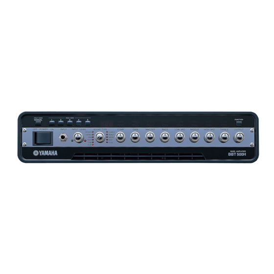
- Page 5 BBT500H (パネルレイアウト) PANEL LAYOUT ●FRONT PANEL(フロントパネル) q Power Switch q 電源スイッチ(POWER) w Input Jack (INPUT) w 入力端子(INPUT) e Input Level Volume (INPUT LEVEL) e 入力レベルボリューム(INPUT LEVEL) r Sound Type Select Switch (SOUND TYPE) r サウンドタイプセレクトスイッチ(SOUND TYPE) t Compressor Volume (COMP) t コンプレッサーボリューム(COMP) y Gain Volume (GAIN) y ゲインボリューム(GAIN) u Master Volume (MASTER) u マスターボリューム(MASTER) i Tone Controls i トーンコントロール (BASS, LOW MID, MIDDLE, HIGH MID, TREBLE) (BASS, LOW MID, MIDDLE, HIGH MID, TREBLE) o Output Volume Level (OUTPUT) o 出力レベルボリューム(OUTPUT)...
- Page 6 BBT500H ●REAR PANEL(リアパネル) !4 Tuner Output (TUNER OUT) !4 チューナー出力端子(TUNER OUT) !5 Effect Loop (FX LOOP) !5 エフェクトループ(FX LOOP) ・ Effect Send Jack (SEND) ・エフェクトセンド端子(SEND) ・ Effect Return Jack (RETURN) ・エフェクトリターン端子(RETURN) ・ Effect Loop Level Switch (LEVEL) ・エフェクトループレベルスイッチ(LEVEL) !6 Headphones Jack (PHONES) !6 ヘッドフォン端子(PHONES) !7 Headphones/Line Out Level Control !7 ヘッドフォン/ラインアウトレベルコントロール (LEVEL) (LEVEL) !8 Line Out Jack !8 ラインアウト端子 (UNBALANCED OUT, BALANCED OUT) (UNBALANCED OUT, BALANCED OUT) !9 Line Out Source Switch !9 ラインアウトソーススイッチ (LINE SOURCE: THRU/PRE EQ/POST EQ) (LINE SOURCE : THRU/PRE EQ/POST EQ) @0 Speaker Simulator Switch ...
- Page 7 BBT500H (分解手順) DISASSEMBLY PROCEDURE トップカバー (所要時間: 約 4 分) Top Cover (Time required: About 4 minutes) [110]のネジ 2 本を外し、サイドパッドを外します。 1-1. Remove the two (2) screws marked [110]. The side (図 1) pad can then be removed. (Fig. 1) [60a]のネジ 4 本と、 [70]のネジ 2 本を外します。...
- Page 8 BBT500H 電源スイッチ Power Switch (所要時間: 約 5 分) (Time required: About 5 minutes) トップカバーを外します。 (1 項参照) 3-1. Remove the top cover. (See procedure 1.) フロント Ass'y を外します(2 項参照) 3-2. Remove the front assembly. (See procedure 2.) 電源スイッチのツメを押えながら、 フロントパネル から電源スイッチを外します。 (図 4)...
- Page 9 BBT500H DM 基板(2/2) DM Circuit Board (2/2) (所要時間: 約 6 分) (Time required: About 6 minutes) [F120]の六角ナット、 [F130]のワッシャーと[F140] 5-1. Remove the Hexagonal nut marked [F120], the Flat の絶縁ナットを外します。 (図 6) washer marked [F130] and the Insulation nut marked ノブ[B]を引き抜いて外します。 (図 6) 六角ナットを外します。...
- Page 10 BBT500H [130] [F80] Hexagonal Nut (六角ナット) (+バインドPタイト) [F80]: Bind Head Tapping Screw-P 3.0X6 MFZN2BL(VA819100) Fig.7 (図7) (ノブ) [130]: Knob (WC936600) Photo.4 (写真4) PW 基板 PW Circuit Board (所要時間: 約 10 分) (Time required: About 10 minutes) トップカバーを外します。 (1 項参照) 7-1. Remove the top cover. (See procedure 1.) フロント...
- Page 11 BBT500H [C120c] [C120b] FET Cover (FETカバー) [C120c] (+バインド小ネジ) [C120]: Bind Head Screw 3.0X8 MFZN2BL(VA295800) Photo.6 (写真6) (+バインド小ネジ) [C120]: Bind Head Screw 3.0X8 MFZN2BL(VA295800) Fig.9(図9) コイル Coil (所要時間: 約 6 分) (Time required: About 6 minutes) 8-1. Remove the top cover. (See procedure 1.) トップカバーを外します。...
- Page 12 BBT500H DC ファン (所要時間: 約 5 分) (Time required: About 5 minutes) 9-1. Remove the top cover. (See procedure 1.) トップカバーを外します。 (1 項参照) 9-2. Remove the nuts marked [C60] and the four (4) [C60]のナットと、 [C50]のネジ 4 本を外します。 screws marked [C50]. (Photo.8, Fig.10) (写真...
- Page 13 BBT500H (LSI 端子機能表) LSI PIN DESCRIPTION HD6413008VF25 (X4196A00) CPU ..................13 AK5383VF (X0578A00) A/D ....................14 AK4393VF-E2 (XW029A00) D/A ..................14 TDA7571 (X4450A00) DIGITAL POWER AMP ..............14 YSS910-V (XV988B00) DSP ....................15 HD6413008VF25 (X4196A00) CPU DM: IC106 NAME FUNCTION NAME FUNCTION...
- Page 14 BBT500H AK5383VF (X0578A00) A/D DM: IC122 NAME FUNCTION NAME FUNCTION VREFL Voltage refernce SDATA Serial data GNDL Ground FSYNC Flame synchronize VCOML Common MCLK Master clock AINL + Analog input + Double fast sampling mode AINL - Analog input -...
- Page 15 BBT500H YSS910-V (XV988B00) DSP6 (Digital Signal Processor) DM: IC104 NAME FUNCTION NAME FUNCTION Power supply (3.3 V) Ground Ground DB13 System master clock input (60 MHz or 30 MHz) DB14 System master clock output (High or 30 MHz) DB15 Vdd5...
- Page 16 BBT500H (IC ブロック図) IC BLOCK DIAGRAM (X3936A00) SN74LVU04APWR SN74LV245APWR (X3693A00) NJM5532M-TE1 (X4980A00) DM: IC116 DM: IC107,109,110 DM: IC112-115 Inverter Transceiver NJM4556AM-TE1 (X5049A00) DM: IC117,118 NJM072BM-E(TE1) (X4543A00) DM: IC301 OP AMP PIN FUNCTION 1 . A OUTPUT 2 . A - INPUT 3 .
- Page 17 BBT500H (X2264A00) IR2153 PW: IC102 Controller LEVEL PULSE SHIFT FILTER DEAD PULSE TIME 15.6V DELAY LOGIC DEAD TIME DETECT TB62726AF (X4257A00) PN: IC401 Driver R-EXT SERIAL-IN CLOCK SERIAL-OUT LATCH ENABLE OUT0 OUT15 OUT1 OUT14 OUT2 OUT13 OUT3 OUT12 OUT4 OUT11...
-
Page 18: Dm(1/2,2/2) Circuit Board (X5383C0)
BBT500H (シート基板図) CIRCUIT BOARDS CONTENTS DM(1/2,2/2) Circuit Board (X5383C0) ..................... 18 PN Circuit Board (X5384A0) ......................22 PW Circuit Board (X4590D0) ......................24 PW Circuit Board (X4590E0) ......................28 Note:See parts list for details of circuit board component parts. 注:シートの部品詳細はパーツリストをご参照ください。... - Page 19 BBT500H LINE OUT LEVEL UNBALANCED SP SIM MIDI BALANCED LINE SOURCE OUTPUT LIMITER to PW-CN107 to PN-CN401 to PN-CN402 to PN-CN403 to PW-CN106 Component side (部品側) 4NA-WC98000-2...
- Page 20 BBT500H Pattern side (パターン側) 4NA-WC98000-2...
- Page 21 BBT500H Pattern side (パターン側) 4NA-WC98000-2...
-
Page 22: Pn Circuit Board (X5384A0)
BBT500H PN Circuit Board RATIO RATIO THRSLD THRSLD PEQ F PEQ F PEQ Q PEQ Q THRSLD THRSLD THRSLD ATTACK ATTACK RELEASE RELEASE C.GAIN C.GAIN KNEE KNEE N.GATE N.GATE BLEND BLEND PEQ G PEQ G PEQ Q PEQ Q FREQ... - Page 23 BBT500H to DM(1/2)-CN104 to DM(1/2)-CN103 to DM(1/2)-CN105 Pattern side (パターン側) 4NA-WC98010-2...
-
Page 24: Pw Circuit Board (X4590D0)
BBT500H PW Circuit Board (X4590D0) SPEAKER AC IN to FAN not installed (U) to Transformer (J,H) to POWER SW to DM( to DM(1/2)-CN Component side (部品側) 4NA-WC89690-3... - Page 25 BBT500H SPEAKER (BRIDGED OUT) not installed (U) to Transformer (J,H) R SW to DM(1/2) -CN102 to DM(1/2)-CN107 to DM(1/2)-CN101 Component side (部品側) 4NA-WC89690-3...
- Page 26 BBT500H Pattern side (パターン側) 4NA-WC89690-2...
- Page 27 BBT500H Pattern side (パターン側) 4NA-WC89690-2...
-
Page 28: Pw Circuit Board (X4590E0)
BBT500H PW Circuit Board (X4590E0) SPEAKER AC IN to FAN not installed (U) to Transformer (J,H) to POWER SW to DM( to DM(1/2)-CN Component side (部品側) 4NA-WC89690-3... - Page 29 BBT500H SPEAKER (BRIDGED OUT) not installed (U) to Transformer (J,H) R SW to DM(1/2) -CN102 to DM(1/2)-CN107 to DM(1/2)-CN101 Component side (部品側) 4NA-WC89690-3...
- Page 30 BBT500H Pattern side (パターン側) 4NA-WC89690-2...
- Page 31 BBT500H Pattern side (パターン側) 4NA-WC89690-2...
- Page 32 BBT500H TEST PROGRAM AND INSPECTIONS Application This specification provides a condition,a method,and a standard for checking BBT500H. Measurement Condition and Note. 2 - 1.Keep in mind that input power supply AC voltage change with destination. it mistakes,parts may break. 2 - 2. AC VOLTAGE...
- Page 33 BBT500H c. Change the position of LINE SOURCE switch THRU → PRE EQ → POST EQ and check the indication of LED "2.6c" → "2.6r" → "2.7L". Change the position of SP SIM switch OFF → LINE → ON and check the indication of LED LED "2.7c"...
- Page 34 BBT500H 4 - 2. INPUT LEVEL VR Check INPUT LEVEL Input point Measure point Load Input level Input frequency Measured value (VR301) INPUT TUNER OUT Min. -22±5dBm 10kΩ -20dBm 1kHz (JK301) (JK102) Max. +12±5dBm 4 - 3. Each output level check 1 FX LOOP LEVEL Input point Measure point Load Input level Input frequency Measured value...
- Page 35 BBT500H 5. Speaker output check 5 - 1.Connection 500W non-guide resistor is connected to speaker jack. 1KHz signal is put into an input jack. Turn off a power supply switch. 5 - 2.Mesurement Volumes are initial setting. Set sound type to FLAT.
- Page 36 BBT500H テストプログラムと検査 適用 ベースアンプヘッド BBT500H の完成品の電気的性能を検査する為の条件、方法、規格について規定します。 測定条件及び注意事項 仕向け地にあった電源コードを使用します。 2 - 1. 完成品のAC 入力電源電圧は、仕向けにより異なるので注意してください。間違えると部品が壊れる恐れがあり ます。 2 - 2. 電源電圧 J 100V ±5V U 120V ±5V H 230V ±5V 2 - 3. スピーカ出力は BTL(BRIDGE)動作による出力となっています。測定系〈オシロスコープ、電圧計)のGND は電 源コードのGND と切り離してください。切り離さない状態にて測定すると、内部の電気部品を破壊する場合が あります。 2 - 4. プリアンプ部分の機能確認(LED 、スイッチ、VR チェック) 、電気特性確認終了後にスピーカ負荷を接続して出 力の確認を行ってください。抵抗負荷は2 Ω500W を使用してください。 2 - 5. 各 VR 、SW の位置を、以下の様に設定してください。 特に指定の無い場合は、この状態で検査を行ってください。 INPUT LEVEL → SOUND TYPE → FLAT COMP → GAIN →...
- Page 37 BBT500H b. LED 表示が、"2." と点滅表示されている状態で、FUNCTION を押すと、LED 表示に "2.0" と表示されます。 MANUAL,HOLD SAVE 1,HOLD SAVE 2, 〜 HOLD SAVE 5 を順番に押していくと、 "2.1" → "2.2" → "2.3" → "2.4" → "2.5" → "2.6L" と表示が変化する事を確認します。 c. LINE SOURCE スイッチの位置を THRU → PRE EQ → POST EQ と変化させると、"2.6c" → "2.6r" → "2.7L" と 変化します。SP SIM スイッチの位置を OFF → LINE → ON と変化させると、"2.7c" → "2.7r" → "2.8L" と変化...
- Page 38 BBT500H 4 - 2. INPUT LEVEL VR チェック INPUT LEVEL 入力点 測定点 負荷 入力レベル 入力周波数 測定値 (VR301) Min. -22±5dBm INPUT TUNER OUT 10kΩ -20dBm 1kHz (JK301) (JK102) Max. +12±5dBm 4 - 3. 各出力レベルチェック 1 FX LOOP LEVEL 入力点 測定点 負荷 入力レベル 入力周波数 測定値 (SW105) 100Hz +12±3dBm TUNER OUT 1kHz as above 10kΩ -20dBm (-20dBm ch.)
- Page 39 BBT500H 5. スピーカ出力確認 5 - 1. 接続 スピーカ端子に2 Ω500W の無誘導抵抗を接続します。 INPUT に1KHz の信号を入力します。 一度電源を切ります。 5 - 2. 測定 ボリュームの設定は初期設定とします。 SOUND TYPE を FLAT に設定します。 電源を入れます。 OUTPUT VR を最小位置より右に回して出力レベルを設定し、その電圧が 28.0 V 以上出る事を確認します。 歪み率は規定しません。 28.0V /2 Ω =400W...
- Page 40 BBT500H ERROR MESSAGE MIDI Receive Buffer Full CAUSE: Too much MIDI data is being received by the BBT500H at one time. SOLUTION: Try reducing the amount of data being sent or, break the data into smaller blocks. Communication Error. CAUSE: An abnormality is detected during MIDI communications.
- Page 41 BBT500H MIDI IMPLIMENTATION CHART YAMAHA [ Bass Amplifier ] Date:23-Dec-2003 Model BBT500H MIDI Implementation Chart Version : 1.0 +----------------------------------------------------------------------+ Transmitted Recognized Remarks Function ... : :-------------------+----------------+----------------+----------------: :Basic Default : 1 - 16, off : memorized :Channel Changed : 1 - 16, off...
- Page 42 BASS AMPLIFIER PARTS LIST (目次) CONTENTS (総組立) OVERALL ASSEMBLY ..........2 (電気部品) ELECTRICAL PARTS ........4-13 Notes : DESTINATION ABBREVIATIONS A : Australian model M : South African model B : British model O : Chinese model C : Canadian model Q : South-east Asia model D : German model T : Taiwan model...
- Page 43 RANK OVERALL ASSEMBLY 総 組 立 BBT500H Overall Assembly 総 組 立 ( J ) BBT500H J (WC94970) Overall Assembly 総 組 立 ( U C ) BBT500H U (WD01870) Overall Assembly 総 組 立 ( E ) BBT500H H,B...
- Page 44 BBT500H PART NO. DESCRIPTION 部 品 名 REMARKS REF NO. RANK V 6 3 2 7 2 0 0 Handle KPBO KAH1D-205 ハ ン ド ル EG340110 Bind Head Screw 4.0X16 MFZN2BL + バ イ ン ド 小 ネ ジ...
- Page 45 BBT500H (電気部品) ELECTRICAL PARTS PART NO. DESCRIPTION 部 品 名 REMARKS REF NO. RANK 電 気 部 品 ELECTRICAL PARTS BBT500H D M シ ー ト WC980000 Circuit Board (1/2,2/2) (X5383C0) WC980100 Circuit Board P N シ ー ト (X5384A0)
- Page 46 BBT500H PART NO. DESCRIPTION 部 品 名 REMARKS REF NO. RANK チ ッ プ セ ラ ( S L ) C0198 US062330 Ceramic Capacitor-SL(chip) 330P 50V J チ ッ プ セ ラ ( S L ) C0199 US062330 Ceramic Capacitor-SL(chip)
- Page 47 BBT500H PART NO. DESCRIPTION 部 品 名 REMARKS REF NO. RANK I C IC104 XV988B00 YSS910-V I C IC105 X2725A00 MSM51V4265E-60TS-K DRAM 4M I C IC105 X2726A00 GLT440L16-40TC I C IC106 X4196A00 HD6413008VF25 I C IC107 X3693A00...
- Page 48 BBT500H PART NO. DESCRIPTION 部 品 名 REMARKS REF NO. RANK チ ッ プ 抵 抗 R0153 RD357560 Carbon Resistor (chip) 56.0K 63M J R0154 RD356100 Carbon Resistor (chip) 1.0K 63M J チ ッ プ 抵 抗 R0155 RD356100 Carbon Resistor (chip) 1.0K 63M J...
- Page 49 BBT500H PART NO. DESCRIPTION 部 品 名 REMARKS REF NO. RANK VV556400 TR303 Transistor 2SC2412K Q,R,S ト ラ ン ジ ス タ VR101 WC928700 Rotary Variable Resistor RD901-20E3-FB-067 ロ ー タ リ ー V R PHONES LEVEL VR301 WC928600 Rotary Variable Resistor RD09L112 ロ...
- Page 50 BBT500H PART NO. DESCRIPTION 部 品 名 REMARKS REF NO. RANK タ ク ト S W WD479300 SW401 Tact Switch SFKHHQW2720-EJ FUNCTION WD479300 タ ク ト S W SW402 Tact Switch SFKHHQW2720-EJ HOLD>UNDO MANUAL タ ク ト S W WD479300...
- Page 51 BBT500H PART NO. DESCRIPTION 部 品 名 REMARKS REF NO. RANK C139 Ceramic Capacitor-B (chip) 2200P 50V K RECT. チ ッ プ セ ラ ( B ) US063220 C140 Ceramic Capacitor-B (chip) 2200P 50V K RECT. チ ッ プ セ ラ ( B )...
- Page 52 BBT500H PART NO. DESCRIPTION 部 品 名 REMARKS REF NO. RANK ベ ー ス ツ キ ポ ス ト CN108 LB918030 Base Post Connector XH 3P TE D101 VT532500 Diode 1SR154-400 TP ダ イ オ ー ド ダ イ オ...
- Page 53 BBT500H PART NO. DESCRIPTION 部 品 名 REMARKS REF NO. RANK R108 RD356100 Carbon Resistor (chip) 1.0K 63M J RECT. チ ッ プ 抵 抗 R109 RD357220 Carbon Resistor (chip) 22.0K 63M J RECT. チ ッ プ 抵 抗 R110...
- Page 54 BBT500H PART NO. DESCRIPTION 部 品 名 REMARKS REF NO. RANK R184 RD357100 Carbon Resistor (chip) 10.0K 63M J RECT. チ ッ プ 抵 抗 R185 RD356330 Carbon Resistor (chip) 3.3K 63M J RECT. チ ッ プ 抵 抗 R186...
- Page 55 BBT500H BBT500H BLOCK DIAGRAM BBT500H OVERALL CIRCUIT DIAGRAM 1/2 ( DM1/2, DM2/2, PN ) JK106 JK107 SW101 SW103 SW102 JK105 JK101 SW105 DM1/2 MIDI JK102 JK104 JK103 SYSTEM RESET DM2/2 CN302 DM1/2 IC301 (4P) CN106 (4P) SRAM 256K JK301 IC115...
- Page 56 BBT500H BBT500H OVERALL CIRCUIT DIAGRAM 2/2 (PW) POWER not installed AC IN CONTROLER REGULATOR +15V REGULATOR +15V to DM-CN107 REGULATOR -15V REGULATOR -15V PHOTO COUPLER REGULATOR +5V Destination WE049900 XY592A00 X5087A00 WE545400 XY593A00 X5088A00 WE049900 XY594A00 X5089A00 to FAN FP : Flame Proof Carbon Resistor (不燃化カーボン抵抗)...