Table of Contents
Advertisement
SERVICE MANUAL
Ver 1.2 2004.08
CX-JS3 is the amplifier, CD player, tape deck
and tuner section in JAX-S3.
TUNER
FM tuning range
87.5 MHz to 108 MHz
FM usable sensitivity (IHF)
16.8 dBf
FM antenna terminal
75 ohms (unbalanced)
AM tuning range
531 kHz to 1602 kHz
AM usable sensitivity
350 µV/m
AM antenna
Loop antenna
AMPLIFIER
Power output
Rated: 32 W + 32 W (6 ohms, T.H.D.
1 %, 1 kHz/DIN 45500)
Reference: 40 W + 40 W (6 ohms,
T.H.D. 10 %, 1 kHz/DIN 45324)
MUSIC POWER: 100 W +100 W
Total harmonic distortion
0.08 % (16 W, 1 kHz, 6 ohms, DIN
AUDIO)
Input
VIDEO/AUX: 400 mV
Outputs
SPEAKER: 6 ohms or more
PHONES: 32 ohms or more
CASSETTE DECK
Track format
4 tracks, 2 channels stereo
Frequency response
50 Hz – 8 kHz
Recording system
AC bias
Heads
Deck A: playback x 1
Deck B: recording/playback x 1,
erase x 1
Sony Corporation
9-877-297-03
2004H05-1
Personel Audio Company
© 2004.08
Published by Sony Engineering Corporation
Model Name Using Similar Mechanism
CD Mechanism Type
CD
Base Unit Name
Section
Optical Block Name
Optical Pick-up Name
Model Name Using Similar Mechanism
Tape deck
Section
Tape Transport Mechanism Type
SPECIFICATIONS
CD PLAYER
Laser
Semiconductor laser (λ = 780 nm)
Emission duration:
continuous
D/A converter
1 bit dual
Signal-to-noise ratio
85 dB (1 kHz, 0 dB)
Harmonic distortion
0.05 % (1 kHz, 0 dB)
GENERAL
Power requirements
230 V AC, 50/60 Hz
Power consumption
65 W
Power consumption
With ECO mode on: 0.25 W
in standby mode
With ECO mode off: 15 W
Dimensions (W x H x D)
280 x 330 x 392.5 mm
Weight
6.6 kg
Specifications and external appearance are subject to change
without notice.
CX-JS3
CX-JN3
CDM74S-K6BD72
BU-K6BD72
KSM-213DCP
KSS-213D
CX-JN3
CWM43FF13
COPYRIGHT
Check copyright laws relevant to recordings from discs, tuner
or tape for the country where the unit is to be used.
Licensed by BBE Sound, Inc. under USP4638258, 5510752
and 5736897.
COMPACT DISC DECK RECEIVER
AEP Model
UK Model
Advertisement
Table of Contents

Related Manuals for Sony Aiwa CX-JS3


Summary of Contents for Sony Aiwa CX-JS3
- Page 1 50 Hz – 8 kHz Recording system AC bias Heads Deck A: playback x 1 Deck B: recording/playback x 1, erase x 1 COMPACT DISC DECK RECEIVER Sony Corporation 9-877-297-03 2004H05-1 Personel Audio Company © 2004.08 Published by Sony Engineering Corporation...
- Page 2 IC pins, etc. OPERATION. REPLACE THESE COMPONENTS WITH • Usable with ordinary solder SONY PARTS WHOSE PART NUMBERS APPEAR AS It is best to use only unleaded solder but unleaded solder may SHOWN IN THIS MANUAL OR IN SUPPLEMENTS PUB- also be added to ordinary solder.
-
Page 3: Table Of Contents
CX-JS3 TABLE OF CONTENTS SERVICING NOTES EXPLODED VIEWS ..........4 7-1. Case Section ..............43 GENERAL 7-2. Front Panel Section-1 ............44 7-3. Front Panel Section-2 ............45 Location of Controls ............6 7-4. Front Panel Section-3 ............46 7-5. Front Panel Section-4 ............47 DISASSEMBLY 7-6. -
Page 4: Servicing Notes
CX-JS3 SECTION 1 SERVICING NOTES NOTES ON LASER DIODE EMISSION CHECK NOTES ON HANDLING THE OPTICAL PICK-UP The laser beam on this model is concentrated so as to be focused BLOCK OR BASE UNIT on the disc reflective surface by the objective lens in the optical The laser diode in the optical pick-up block may suffer electro- pick-up block. - Page 5 CX-JS3 SERVICE POSITION – CD mechanism deck – main board (CN691) Connect wire (flat type) (19 core) to main board (CN691) and BD board (CN710). BD board (CN710) – Tape mechanism deck – panel board (CN601) main board (CN301) Connect wire (flat type) (13 core) to panel board (CN601) and mechanical deck.
-
Page 6: General
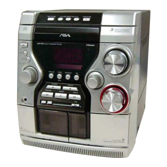
CX-JS3 SECTION 2 This section is extracted from instruction manual. GENERAL • LOCATION OF CONTROLS 5 MULTI JOG # TREBLE Main unit: front When used in combination with ENTER and MULTI JOG, Enhances high frequency sound. Refer to the pages indicated in parentheses for details. CD: selects a track and Repeat/Shuffle/Programmed $ cPLAY/PRESET playback. - Page 7 CX-JS3 Remote control 9 DISC SKIP SPECTRUM Changes the spectrum analyzer display. Select a disc. Refer to the pages indicated in parentheses for details. 0 c/d TUNER MODE Switches between stereo or monaural FM reception. When the unit is turned off: activates or deactivates DEMO.
-
Page 8: Disassembly
CX-JS3 SECTION 3 DISASSEMBLY • This set can be disassembled in the order shown below. 3-1. DISASSEMBLY FLOW Note 1: The process described in can be performed in any order. Note 2: Without completing the process described in , the next process can not be performed. 3-2. -
Page 9: Case (Side-L/R)
CX-JS3 Note: Follow the disassembly procedure in the numerical order given. 3-2. CASE (SIDE-L/R) 2 two screws 5 case (side-L) × (BVTP3 1 two case screws 2 two screws × (BVTP3 1 two case screws 1 case screw 5 case (side-R) 1 case screw 3-3. -
Page 10: Tray Panel
CX-JS3 3-4. TRAY PANEL 1 Turn the loading gear in the direction of arrow A . 2 Pull-out the disc table. 3 four claws 4 tray panel 3-5. CD MECHANISM DECK (CDM74S-K6BD72) 5 CD mechanism deck (CDM74S-K6BD72) 1 wire (flat type) (19 core) (CN691) 2 connector (CN701) -
Page 11: Front Panel Section
CX-JS3 3-6. FRONT PANEL SECTION 2 headphone board 3 wire (flat type) (11 core) 1 screw (CN694) (BVWHTP) 6 connector (CN101) 4 connector (CN302) 4 connector (CN301) 7 front panel section 5 three screws × (BVTP3 3-7. MECHANICAL DECK (CWM43FF13) 3 clamp 4 mechanical deck (CWM43FF13) -
Page 12: Rear Cabinet Section
CX-JS3 3-8. REAR CABINET SECTION 3 rear cabinet section 1 wire (flat type) (15 core) (CN802) 2 three screws × (BVTP3 2 screw × (BVTP3 3-9. PT BOARD, MAIN BOARD 3 screw × (BVTP3 2 screw 5 two screws × (BVTT3 5 two screws ×... -
Page 13: Motor (Tb) Board
CX-JS3 3-10. TABLE ASSY 5 two claws 4 hook 3 wire (flat type) (5 core) (CN702) 1 Turn the loading gear 2 Pull-out the table assy. in the direction of arrow A . 6 table assy 3-11. MOTOR (TB) BOARD 1 screw (PTPWH M2.6) 2 table (loading) -
Page 14: Motor (Ld) Board
CX-JS3 3-12. MOTOR (LD) BOARD 3 two screws (BTTP M2.6) 4 motor (LD) board 2 connector (CN704) 1 belt (loading) 3-13. BASE UNIT (BU-K6BD72) 5 base unit (BU-K6BD72) 4 four insulators 3 four coil springs (insulator) 2 four stoppers (BU) 1 four screws (BTTP M2.6) -
Page 15: Motor Gear Assy (Sled) (M701), Bd Board
CX-JS3 3-14. MOTOR GEAR ASSY (SLED) (M701), BD BOARD 7 gear (A) 6 claw 8 gear (B) 2 two screws (P2 × 3) 5 wire (flat type) (16 core) (CN708) qa BD board 0 motor gear assy (SLED) (M701) 1 Remove two solders. -
Page 16: Test Mode
CX-JS3 SECTION 4 TEST MODE MC COLD RESET FUNCTION CHANGE MODE • The cold reset clears all data including preset data stored in the • Select either TV, VIDEO or AUX (MD) of the external function RAM to initial conditions. Execute this mode when returning input. -
Page 17: Electrical Adjustments
CX-JS3 SECTION 5 ELECTRICAL ADJUSTMENTS Note: Clear RF signal waveform means that the shape “ ◊ ” can be clearly CD TEST MODE CD SECTION distinguished at the center of the waveform. • This mode can run the CD sled motor freely. Use this mode, for instance, when cleaning the pickup. -
Page 18: Diagrams
CX-JS3 SECTION 6 DIAGRAMS 6-1. BLOCK DIAGRAM – CD Section – OPTICAL PICK-UP BLOCK CD DSP (KSM-213DCP) IC721 FIN2 LCHO (Page 20) DETECTOR EFMIN ERROR RF AMP CONVERTER CORRECT RCHO R-CH FIN1 ASDFIN ASDACK EXTERNAL AUDIO IN ASLRCK DATA DATACK SERIAL OUT LRSY PH, BH... -
Page 19: Block Diagram - Tuner/Tape/Panel Section
CX-JS3 6-2. BLOCK DIAGRAM – TUNER/TAPE/PANEL Section – PB SWITCH (Page 20) L-CH Q301 (PB) (DECK-A) R-CH R-CH FM/AM TUNER PACK FM 75Ω L-CH (Page 20) FM ANT (COAXIAL) PB SWITCH R-CH R-CH Q303 L-CH AM LOOP AM ANT MUTING Q305 R-CH R-CH... -
Page 20: Block Diagram - Amp/Power Supply Section
CX-JS3 6-3. BLOCK DIAGRAM – AMP/POWER SUPPLY Section – SWITCHING Q231 OUTPUT LEVEL DETECT R-CH R-CH SPEANA Q233, 234 (Page 19) R-CH FEED BACK SWITCH SWITCHING Q643 Q232 OUTPUT LEVEL J602 DBFB CONTROL R-CH DETECT Q641 Q235 VIDEO/AUX R-CH CURRENT MIRROR Q105, 107 BASS BOOST ENHANCER... -
Page 21: Note For Printed Wiring Boards And Schematic Diagrams
CX-JS3 6-4. NOTE FOR PRINTED WIRING BOARDS AND SCHEMATIC DIAGRAMS • Circuit Boards Location Note on Printed Wiring Board: Note on Schematic Diagram: SENSOR board • All capacitors are in µF unless otherwise noted. pF: µµF • X : parts extracted from the component side. PT board •... -
Page 22: Printed Wiring Board - Bd Section
CX-JS3 6-5. PRINTED WIRING BOARD – BD Section – • :Uses unleaded solder. See page 21 for Circuit Boards Location. M702 (SPINDLE) BD BOARD S701 (LIMIT IN) − IC722 OPTICAL M701 PICK-UP (SLED) BLOCK (KSM-213DCP) − CN710 (VC) TP (FE) TP (TE) (RF) MAIN... -
Page 23: Schematic Diagram - Bd Section
CX-JS3 6-6. SCHEMATIC DIAGRAM – BD Section – • See page 38 for IC Block Diagram. • See page 38 for Waveforms. R732 R731 2.2k R721 R722 C752 C753 R707 C709 C746 C742 C708 R729 C744 C754 C745 C750 C751 Q701 KTN2907AS R726... -
Page 24: Printed Wiring Boards - Changer Section
CX-JS3 6-7. PRINTED WIRING BOARDS – CHANGER Section – • :Uses unleaded solder. See page 21 for Circuit Boards Location. SW BOARD SENSOR BOARD CN751 IC731 S751 MAIN BOARD OPEN/CLOSE CN692 DETECT (Page 30) CLOSE DRIVER BOARD C715 OPEN Q731 CN701 C731 CN705... -
Page 25: Schematic Diagram - Changer Section
CX-JS3 6-8. SCHEMATIC DIAGRAM – CHANGER Section – • See page 38 for IC Block Diagrams. LOADING MOTOR DRIVE IC701 BA6956AN R702 R701 CN721 CN704 LM-2 LM-2 D701 M751 C751 LM-1 LM-1 MTZJ-T-77 0.01 (LOADING) 5.1A S711 DISC TRAY ADDRESS DETECT CN703 TABLE MOTOR DRIVE... -
Page 26: Schematic Diagram - Main Section (1/4)
CX-JS3 6-9. SCHEMATIC DIAGRAM – MAIN Section (1/4) – (1/4) WH013 R017 D019 0.47 EGP20D VM(AC) VM(AC) C007 D021 D022 D020 VH(AC) 3300 EGP20D EGP20D EGP20D VH(AC) C011 C012 C033 VL(AC) VL(AC) GND(M) (Page 37) FIL-1 D009 FIL-2 D5SBA20 R026 R027 R028 R029... -
Page 27: Schematic Diagram - Main Section (2/4)
CX-JS3 6-10. SCHEMATIC DIAGRAM – MAIN Section (2/4) – D107 (2/4) R123 Q101,103 R131 1SS184 6.8k 4.7k PRE DRIVE C127 1000p R119 2.2k C133 1000p Q123 2SD2619 R117 R121 C105 C181 2.2k FINAL DRIVE D105 R183 1SS181 3.9k Q103 R133 C121 OUT-L 2SA1235... -
Page 28: Schematic Diagram - Main Section (3/4)
CX-JS3 6-11. SCHEMATIC DIAGRAM – MAIN Section (3/4) – • See page 38 for IC Block Diagram. • See page 38 for Waveforms. (3/4) SP-A-GND C687 0.01 TU/AUX-A-GND CD-A-GND FR-A-GND FUNC-A-GND CD-D-GND CD-P-GND FR-D-GND CD-VM CD-VM TP601 JR601 JR611 R653 (Page 27) (AEP,UK) HOLD... -
Page 29: Schematic Diagram - Main Section (4/4)
CX-JS3 6-12. SCHEMATIC DIAGRAM – MAIN Section (4/4) – • See page 38 for IC Block Diagrams. (EXCEPT AEP,UK) (4/4) CN801 FM 75Ω FM/AM (COAXIAL) PLL-CE TUNER PACK R687 R676 R677 R678 SUPPLIED WITH 4.7k 2.2k TUNED THE ASSEMBLED TUNED BLOCK C679 STEREO... -
Page 30: Printed Wiring Board - Main Section
CX-JS3 6-13. PRINTED WIRING BOARD – MAIN Section – • See page 21 for Circuit Boards Location. :Uses unleaded solder. MAIN BOARD (AEP, UK) R809 R810 BD BOARD R812 JW802 CN710 JW661 (Page 22) JW803 R807 JW662 EXCEPT JW610 JW609 JW618 JW805 JW611... -
Page 31: Printed Wiring Board - Hp Section
CX-JS3 6-14. PRINTED WIRING BOARD – HP Section – • 6-15. SCHEMATIC DIAGRAM – HP Section – See page 21 for Circuit Boards Location. :Uses unleaded solder. MAIN BOARD WH201 (Page 30) FB221 C906 HEADPHONE WH230 WH230 JW222 C906 C907 J221 100p 100p... -
Page 32: Printed Wiring Board - Panel Section
CX-JS3 6-16. PRINTED WIRING BOARD – PANEL Section – • See page 21 for Circuit Boards Location. :Uses unleaded solder. • Semiconductor Location Ref. No. Location C908 R932 R927 D101 C909 R908 D623 D622 R905 D201 C905 (Page 30) D501 IC801 D620 D621... -
Page 33: Schematic Diagram - Panel Section
CX-JS3 6-17. SCHEMATIC DIAGRAM – PANEL Section – • • See page 38 for IC Block Diagram. See page 38 for Waveforms. FL901 FLUORESCENT INDICATOR TUBE JW902 R943 R942 1.8k 1.8k JW901 C916 C917 R944 6.8k JR903 D201 R221 CN701 1SS133 R707 CD_CE... -
Page 34: Printed Wiring Boards - Key Section
CX-JS3 6-18. PRINTED WIRING BOARDS – KEY Section – • :Uses unleaded solder. See page 21 for Circuit Boards Location. KEY BOARD LED901 STANDBY/ON JR803 (AEP) JR807 S315 (UK) JR808 POWER JR809 (CIS) S801 S307 VOLUME MODE S301 − 315, S317 −... -
Page 35: Schematic Diagram - Key Section
CX-JS3 6-19. SCHEMATIC DIAGRAM – KEY Section – R801 R803 R809 R811 S801 S803 VOLUME BASS R802 C801 C802 R804 R810 C805 C806 R812 1000p 1000p 1000p 1000p R301 R302 R303 R304 R305 R306 1.2k 1.2k S306 S301 S302 S303 S304 S305 R805... -
Page 36: Printed Wiring Board - Pt Section
CX-JS3 6-20. PRINTED WIRING BOARD – PT Section – • See page 21 for Circuit Boards Location. :Uses unleaded solder. PT BOARD JW204 CN091 JW214 (AC IN) PR093 PT002 POWER TRANSFORMER (MAIN) RY001 ∗ MAIN BOARD PT011 WH013 POWER TRANSFORMER ∗... -
Page 37: Schematic Diagram - Pt Section
CX-JS3 6-21. SCHEMATIC DIAGRAM – PT Section – PT002 POWER TRANSFORMER WH093 (MAIN) VM(AC) VM(AC) ∗ VH(AC) NOT REPLACEABLE: BUILT IN TRANSFORMER VH(AC) VL(AC) ∗ VL(AC) GND(M) FIL-1 (Page 26) FIL-2 P-ON C091 VSTBY RY001 PT011 POWER TRANSFORMER D091 (SUB) CN091 1SS181 (AC IN) - Page 38 CX-JS3 • Waveforms • IC Block Diagrams – PANEL Board – – BD Board – – BD Board – – MAIN Board – IC721 LC78646E-E 1 IC721 4 (RF) (CD Play Mode) qa L311 6 , 7 (REC Mode) qf IC901 qd (XT2) 78 77 76 75 74 73 72 71 69 68 67 66 65 64 63 62 61...
- Page 39 CX-JS3 – DRIVER Board – IC701, 712 BA6956AN CONTROL LOGIC – MAIN Board – IC601 BD3881FV BASS BASS VOLUME TREBLE LOGIC CONTROL VOLUME TREBLE...
- Page 40 CX-JS3 IC671 NJM2156M (TE2) IC672 BU2092F-E2 16 15 14 13 12 11 19 18 17 16 12 11 12 BIT BIAS CONTROL SHIFT CIRCUIT REGISTER OUTPUT 12 BIT BUFFER STORAGE (OPEN DRAIN) REGISTER MACH3 5 6 7 8 9 – PANEL Board – IC501 MM1614A CURRENT BIAS...
-
Page 41: Ic Pin Function Description
CX-JS3 6-22. IC PIN FUNCTION DESCRIPTION • PANEL BOARD IC901 LC876796B-51F8 (SYSTEM CONTROLLER) Pin No. Pin Name Description SYS-MUTE Line muting on/off control signal output terminal RDS DO RDS serial data input from the FM/AM tuner unit TU/EVOL DO Serial data output to the FM/AM tuner unit, motor/plunger driver and electrical volume CD RESET Reset signal output to the CD DSP CD CE... - Page 42 CX-JS3 Pin No. Pin Name Description Deck-A cassette detection signal input and segment drive signal output to the fluorescent A HALF/S12 indicator tube Deck-A mode detection signal input and segment drive signal output to the fluorescent indicator A MODE/S13 tube 56 to 67 S14 to S25 Segment drive signal output to the fluorescent indicator tube...
-
Page 43: Exploded Views
CX-JS3 SECTION 7 EXPLODED VIEWS NOTE: • -XX and -X mean standardized parts, so they • Items marked “*” are not stocked since they The components identified by mark 0 or dotted line with mark may have some difference from the original are seldom required for routine service. -
Page 44: Front Panel Section-1
CX-JS3 7-2. FRONT PANEL SECTION-1 not supplied not supplied front panel section -2 Ref. No. Part No. Description Remark Ref. No. Part No. Description Remark 4-245-177-01 ROTARY (JOG), KNOB 4-245-176-01 PLATING, KNOB ROTARY (BASS) 4-245-179-01 ROTARY (TRE), KNOB 1-796-485-51 DECK, MECHANICAL (CWM43FF13) 4-245-182-01 PLATING, KNOB ROTARY (VOL) 7-685-647-79 SCREW +BVTP 3X10 TYPE2 N-S... -
Page 45: Front Panel Section-2
CX-JS3 7-3. FRONT PANEL SECTION-2 front panel section -3 Ref. No. Part No. Description Remark Ref. No. Part No. Description Remark 1-688-379-11 CD KEY BOARD 1-769-857-11 WIRE (FLAT TYPE) (5 CORE) 1-688-400-12 HEADPHONE BOARD A-4747-704-A KEY BOARD, COMPLETE (AEP, UK) 3-229-336-01 SCREW, +BVWH TAPPING A-4747-829-A KEY BOARD, COMPLETE (CIS) 4-245-189-01 REFLECTOR, REMOTE CONTROL... -
Page 46: Front Panel Section-3
CX-JS3 7-4. FRONT PANEL SECTION-3 front panel section -4 Ref. No. Part No. Description Remark Ref. No. Part No. Description Remark 4-245-193-01 RING (BASS) 4-245-172-01 KEY (FUN) (TAPE A/B. TUNER BAND. 4-245-199-11 WINDOW, DISPLAY VIDEO/AUX. CD. B. x) 4-245-277-31 DISPLAY, WINDOW (CIS) X-4955-560-1 KEY ASSY (POWER) 4-233-980-01 RUBBER FOOT X-4955-571-1 KEY ASSY (OPE) (m. -
Page 47: Front Panel Section-4
CX-JS3 7-5. FRONT PANEL SECTION-4 Ref. No. Part No. Description Remark Ref. No. Part No. Description Remark 4-245-198-01 WINDOW (2), CASSETTE 4-245-161-61 CABINET, FRONT (CIS) 4-245-160-01 BOX, CASSETTE (2) 4-231-836-01 SPRING (HEART CAM-A) 4-245-196-01 SPRING (R), TORSION COIL 4-231-841-01 SPRING (HEART CAM-B) 4-245-197-01 WINDOW (1), CASSETTE 4-224-104-41 DAMPER 4-245-159-01 BOX, CASSETTE (1) -
Page 48: Chassis Section
CX-JS3 7-6. CHASSIS SECTION not supplied not supplied not supplied not supplied not supplied PT002 not supplied not supplied not supplied not supplied The components identified by mark 0 or dotted line with mark 0 are critical for safety. Replace only with part number specified. Ref. -
Page 49: Cd Mechanism Deck Section-1 (Cdm74S-K6Bd72)
CX-JS3 7-7. CD MECHANISM DECK SECTION-1 (CDM74S-K6BD72) M741 CD mechanism deck section -2 Ref. No. Part No. Description Remark Ref. No. Part No. Description Remark 4-243-815-01 TABLE (LOADING) 1-687-134-11 MOTOR (TB) BOARD 4-243-816-01 TRAY 4-218-252-61 SCREW (+PTPWH M2.6), FLOATING 4-218-253-21 SCREW (M2.6), +BTTP 3-321-598-01 SHEET (BA) 1-687-132-11 SENSOR BOARD 4-245-570-01 GEAR (JOINT) -
Page 50: (Cdm74S-K6Bd72)
CX-JS3 7-8. CD MECHANISM DECK SECTION-2 (CDM74S-K6BD72) S711 M751 CD mechanism deck section -3 Ref. No. Part No. Description Remark Ref. No. Part No. Description Remark 4-218-252-61 SCREW (+PTPWH M2.6), FLOATING 3-016-533-11 WASHER (FR), STOPPER 4-244-034-01 BELT (LOADING) 4-244-108-01 GEAR, SWING 4-224-613-01 GEAR (SHAFT) 4-224-608-01 COLLAR, SWING 4-218-253-31 SCREW (M2.6), +BTTP... -
Page 51: (Cdm74S-K6Bd72)
CX-JS3 7-9. CD MECHANISM DECK SECTION-3 (CDM74S-K6BD72) BU-K6BD72 Ref. No. Part No. Description Remark Ref. No. Part No. Description Remark X-4955-707-1 PULLEY (A5) ASSY, CHUCKING 4-227-549-11 INSULATOR 1-471-035-11 MAGNET ASSY 4-227-045-31 SPRING (INSULATOR), COIL 4-231-151-01 STOPPER (BU) 4-231-189-01 PULLEY (B), CHUCKING 4-218-252-61 SCREW (+PTPWH M2.6), FLOATING 4-218-253-31 SCREW (M2.6), +BTTP 4-243-817-01 CHASSIS... -
Page 52: Base Unit Section (Bu-K6Bd72)
CX-JS3 Ver 1.1 7-10. BASE UNIT SECTION (BU-K6BD72) not supplied (M702) not supplied (M701) The components identified by mark 0 or dotted line with mark 0 are critical for safety. Replace only with part number specified. Ref. No. Part No. Description Remark Ref. -
Page 53: Electrical Parts List
CX-JS3 SECTION 8 ELECTRICAL PARTS LIST NOTE: • Due to standardization, replacements in the • Items marked “*” are not stocked since they The components identified by mark 0 or dotted line with mark parts list may be different from the parts speci- are seldom required for routine service. - Page 54 CX-JS3 CD KEY DRIVER HEADPHONE Ref. No. Part No. Description Remark Ref. No. Part No. Description Remark R727 1-216-809-11 METAL CHIP 1/10W C751 1-162-306-11 CERAMIC 0.01uF R728 1-216-841-11 METAL CHIP 1/10W C752 1-164-159-21 CERAMIC 0.1uF R729 1-216-834-11 METAL CHIP 1/10W <...
- Page 55 CX-JS3 HEADPHONE MAIN Ref. No. Part No. Description Remark Ref. No. Part No. Description Remark < CONNECTOR > R806 1-216-833-11 METAL CHIP 1/10W WH230 1-816-818-11 HLDR, WIRE 2.5-5P R807 1-216-797-11 METAL CHIP 1/10W R808 1-216-797-11 METAL CHIP 1/10W ************************************************************** R809 1-216-833-11 METAL CHIP 1/10W A-4747-704-A KEY BOARD, COMPLETE (AEP, UK)
- Page 56 CX-JS3 MAIN Ref. No. Part No. Description Remark Ref. No. Part No. Description Remark C022 1-126-933-11 ELECT 100uF C206 1-162-974-11 CERAMIC CHIP 0.01uF C207 1-162-970-11 CERAMIC CHIP 0.01uF C023 1-126-948-11 ELECT 100uF C208 1-162-970-11 CERAMIC CHIP 0.01uF C026 1-126-947-11 ELECT 47uF C230 1-119-850-11 ELECT...
- Page 57 CX-JS3 MAIN Ref. No. Part No. Description Remark Ref. No. Part No. Description Remark C652 1-162-964-11 CERAMIC CHIP 0.001uF C904 1-127-888-11 CERAMIC CHIP 0.1uF C905 1-127-888-11 CERAMIC CHIP 0.1uF C653 1-162-964-11 CERAMIC CHIP 0.001uF C654 1-162-927-11 CERAMIC CHIP 100PF < CONNECTOR > C655 1-162-964-11 CERAMIC CHIP 0.001uF...
- Page 58 CX-JS3 MAIN Ref. No. Part No. Description Remark Ref. No. Part No. Description Remark JR615 1-216-864-11 SHORT CHIP D291 8-719-820-05 DIODE 1SS181-TE85L JR616 1-216-864-11 SHORT CHIP D292 8-719-801-78 DIODE 1SS184-TE85L JR618 1-216-864-11 SHORT CHIP D301 8-719-820-05 DIODE 1SS181-TE85L JR619 1-216-864-11 SHORT CHIP D661 8-719-083-60 DIODE UDZSTE-174.7B JR620...
- Page 59 CX-JS3 MAIN Ref. No. Part No. Description Remark Ref. No. Part No. Description Remark Q234 8-729-120-28 TRANSISTOR 2SC3052EF-T1-LEF R036 1-216-836-11 METAL CHIP 1/10W Q235 8-729-600-22 TRANSISTOR 2SA1235TP-1EF R038 1-216-296-00 SHORT CHIP R041 1-216-845-11 METAL CHIP 100K 1/10W Q281 8-729-216-31 TRANSISTOR 2SA1163G-TE85L R042 1-216-845-11 METAL CHIP...
- Page 60 CX-JS3 MAIN Ref. No. Part No. Description Remark Ref. No. Part No. Description Remark R126 1-216-823-11 METAL CHIP 1.5K 1/10W R257 1-216-841-11 METAL CHIP 1/10W R258 1-216-841-11 METAL CHIP 1/10W R127 1-216-809-11 METAL CHIP 1/10W R259 1-216-841-11 METAL CHIP 1/10W R128 1-216-809-11 METAL CHIP 1/10W...
- Page 61 CX-JS3 MAIN MOTOR (LD) Ref. No. Part No. Description Remark Ref. No. Part No. Description Remark R625 1-216-828-11 METAL CHIP 3.9K 1/10W R688 1-216-816-11 METAL CHIP 1/10W (AEP, UK) R691 1-216-837-11 METAL CHIP 1/10W R626 1-216-827-11 METAL CHIP 3.3K 1/10W R692 1-216-833-11 METAL CHIP 1/10W...
- Page 62 CX-JS3 MOTOR (TB) PANEL Ref. No. Part No. Description Remark Ref. No. Part No. Description Remark 1-687-134-11 MOTOR (TB) BOARD C926 1-164-156-11 CERAMIC CHIP 0.1uF C927 1-164-156-11 CERAMIC CHIP 0.1uF ***************** C930 1-164-156-11 CERAMIC CHIP 0.1uF < CONNECTOR > C931 1-164-156-11 CERAMIC CHIP 0.1uF CN742...
- Page 63 CX-JS3 PANEL Ref. No. Part No. Description Remark Ref. No. Part No. Description Remark JR219 1-216-864-11 SHORT CHIP R203 1-216-849-11 METAL CHIP 220K 1/10W JR220 1-216-864-11 SHORT CHIP R204 1-216-840-11 METAL CHIP 1/10W JR401 1-216-864-11 SHORT CHIP R205 1-216-829-11 METAL CHIP 4.7K 1/10W R206...
- Page 64 CX-JS3 PANEL Ref. No. Part No. Description Remark Ref. No. Part No. Description Remark R640 1-249-417-11 CARBON 1/4W R942 1-247-837-81 CARBON 1.8K 1/4W R641 1-249-417-11 CARBON 1/4W R943 1-247-837-81 CARBON 1.8K 1/4W R944 1-249-427-11 CARBON 6.8K 1/4W R642 1-249-417-11 CARBON 1/4W R945 1-249-427-11 CARBON...
- Page 65 CX-JS3 Ver 1.2 SENSOR Ref. No. Part No. Description Remark Ref. No. Part No. Description Remark < CONNECTOR > WH093 1-817-363-11 HOLDER, WIRE 11P ************************************************************** 1-687-132-11 SENSOR BOARD ************** < CONNECTOR > CN731 1-785-329-21 PIN, CONNECTOR (LIGHT ANGLE) 3P < IC > IC731 6-600-022-01 IC RPI-576 **************************************************************...
- Page 66 CX-JS3 REVISION HISTORY Clicking the version allows you to jump to the revised page. Also, clicking the version at the upper right on the revised page allows you to jump to the next revised page. Ver. Date Description of Revision 2003.04 2004.04 Changing of BASE UNIT SECTION in EXPLODED VIEWS...