Table of Contents
Advertisement
www.freeservicemanuals.info
SERVICE MANUAL
Ver 1.2 2003.09
CX-LMN5 is the Amplifier, CD player, Tape
Deck and Tuner section in XR-MN5.
MAIN UNIT CX-LMN5
TUNER
FM tuning range
FM usable sensitivity (IHF)
FM antenna terminal
AM tuning range
AM usable sensitivity
AM antenna
AMPLIFIER
Power output
Input
Outputs
9-877-183-03
2003I16-1
© 2003.09
CASSETTE DECK
Track format
Frequency response
87.5 MHz to 108 MHz
Recording system
16.8 dBf
Heads
75 Ω (unbalanced)
531 kHz to 1602 kHz (9 kHz Step)
CD PLAYER
(AEP, UK)
Laser
530 kHz to 1710 kHz (10kHz Step)
(EXCEPT AEP, UK)
D/A converter
531 kHz to 1710 kHz (9kHz Step)
Signal-to-noise ratio
(EXCEPT AEP, UK)
Wow and flutter
350 µV/m
Loop antenna
GENERAL
Power requirements
Rated: 64 W + 64 W (6 Ω, T.H.D.
1 %, 1 kHz/DIN 45500)
Reference: 80 W + 80 W (6 Ω, T.H.D.
10 %, 1 kHz/DIN 45324)
MUSIC POWER: 220 W + 220 W
AUX IN: 1.4 V
SPEAKERS: 6 Ω or more
PHONES: 32 Ω or more
Power consumption
Sony Corporation
Home Audio Company
Published by Sony Engineering Corporation
Published in Heiloo, Holland.
CX-LMN5
Model Name Using Similar Mechanism
CD Mechanism Type
CD
Section
Base Unit Name
Optical Pick-up Name
Model Name Using Similar Mechanism
TAPE
Section
Tape Transport Mechanism Type
SPECIFICATIONS
4 tracks, 2 channels stereo
100 Hz – 10000 Hz
AC bias
Recording/playback × 1, erase × 1
Semiconductor laser (λ = 800 nm)
Emission duration: continuous
1 bit dual
85 dB (1 kHz, 0 dB)
Unmeasurable
230 V AC, 50/60 Hz (AEP, UK)
120 V AC, 60 Hz (US, CND, TW)
120 V/220 V/230-240 V AC,
50/60 Hz (E)
220 V AC, 50/60 Hz (KR)
110-240 V AC, 50/60 Hz (TH)
220-240 V AC, 50/60 Hz (SP)
240 V AC, 50/60 Hz (AUS, TW)
85 W (EXCEPT US, CND)
80 W (US, CND)
MICRO HI-FI COMPONENT SYSTEM
US Model
Canadian Model
AEP Model
UK Model
E Model
Australian Model
NEW
CDM69BV-30CBD64NS
BU-30CBD64NS
A-MAX.3
NEW
CMAL1Z240A
Power consumption in standby mode
with ECO mode on: 0.26 W (EXCEPT E)
0.35W (E)
0.25 W (US,CND)
0.26 W (AEP,UK)
0.26 W(TH,KR)
0.35 W(OTHER)
with ECO mode off:15 W (EXCEPT E)
18 W(E)
16 W (US,CND)
15 W (AEP,UK)
18 W (TH,KR)
18 W (OTHER)
Approx. 190 × 277 × 353 mm
Dimensions (w/h/d)
Mass
Approx. 6.8 kg
Supplied accessories:
FM antenna (1)
AM antenna (1)
Speaker cords (2)
Remote commander (1)
Batteries (2)
Specifications and external appearance are subject to change
without notice.
• Abbreviation
AUS : Australian model.
CND : Canadian model.
SP
: Singapore model.
TW : Taiwan model.
KR
: Korean model.
TH
: Thai model.
9/6/15
Advertisement
Table of Contents

Related Manuals for Sony CX-LMN5


Summary of Contents for Sony CX-LMN5
-
Page 1: Cd Mechanism Deck Section
US Model Canadian Model Ver 1.2 2003.09 AEP Model UK Model E Model Australian Model CX-LMN5 is the Amplifier, CD player, Tape Deck and Tuner section in XR-MN5. Model Name Using Similar Mechanism CD Mechanism Type CDM69BV-30CBD64NS Section Base Unit Name... -
Page 2: Table Of Contents
LIST ARE CRITICAL TO SAFE OPERATION. REPLACE THESE COMPONENTS WITH SONY PARTS WHOSE PART NUMBERS REMPLACER CES COMPOSANTS QUE PAR DES PIÈSES SONY APPEAR AS SHOWN IN THIS MANUAL OR IN SUPPLEMENTS DONT LES NUMÉROS SONT DONNÉS DANS CE MANUEL OU PUBLISHED BY SONY. -
Page 3: Servicing Notes
9/6/15 CX-LMN5 SECTION 1 SERVICING NOTES Notes on chip component replacement CAUTION • Never reuse a disconnected chip component. Use of controls or adjustments or performance of procedures • Notice that the minus side of a tantalum capacitor may be dam- other than those specified herein may result in hazardous aged by heat. -
Page 4: General
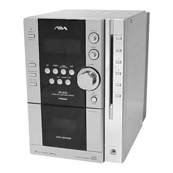
9/6/15 CX-LMN5 SECTION 2 GENERAL This section is extracted from instruction manual. PARTS AND CONTROLS 3 ECO/RDS (8, 14-16) 8 i-Bass/DEMO (4, 9) Main unit: front Sets the ECO mode on or off. Produces rich and clear low frequency sound. -
Page 5: Adjustments Before Operation
9/6/15 CX-LMN5 Remote commander TUNER MODE (15) SLEEP (21) Switches between stereo or monaural FM reception. Selects sleep-timer mode. Refer to the pages indicated in parentheses for details. 7 SHIFT REV MODE (17, 18, 22) Selects a reverse mode. -
Page 6: Disassembly
9/6/15 CX-LMN5 SECTION 3 DISASSEMBLY • This set can be disassembled in the order shown below. SIDE PANEL (L) (R), TOP PANEL, CASSETTE PANEL BACK PANEL MAIN BOARD SECTION CD MECHANISM SECTION FRONT PANEL SECTION POWER TRANSFORMER CD MECHANISM DECK... -
Page 7: Side Panel (L)(R), Top Panel, Back Panel
9/6/15 CX-LMN5 Note: Follow the disassembly procedure in the numerical order given. 3-1. Side Panel (L)(R), Top Panel, Back Panel qf screw (+BVTP3 × 10) 7 screw (+BVTP3 × 10) q; top panel qh w ire (flat type) 15p /11P... -
Page 8: Front Panel Section
9/6/15 CX-LMN5 3-3. Front Panel Section 2 w ire (flat type) 8p ( cassette deck mechanism ) 9 front panel section 1 w ire (flat type) 17p (CN904) 7 screw (QT2+3 × 10) 8 two claws 3 connector (CN302) -
Page 9: Cassette Deck Mechanism
9/6/15 CX-LMN5 3-5. Cassette Deck Mechanism 3 three screws (+BVTP3 × 10) 4 cassette deck mechanism 1 screw (+BVTP3 × 10) 2 shield (DECK) 3-6. Cassette Panel 3 claw 3 claw 4 cassette panel Published in Heiloo, Holland. -
Page 10: Power Transformer
9/6/15 CX-LMN5 3-7. Power Transformer 4 connector 3 connector (CN256) (CN252/ 254) 1 four s-screws (ITC +4- 10R) 5 power transformer 2 connector (CN257) 3-8. MAIN Board Section qa MAIN board 7 connector (CN294) 9 four s-screws (IT3B +3 - 8CU) -
Page 11: Cd Mechanism Deck (Cdm69Bv-30Cbd64Ns)
9/6/15 CX-LMN5 3-9. CD Mechanism Deck (CDM69BV-30CBD64NS) 1 three screws (QT2+3 × 10) 2 holder(CD B) 3 four screws (+BVTP3 × 10) 4 CD mechanism deck (CDM69BV-30CBD64NS) 3-10. Base Unit Section 2 screw (+PTPWH) (M2) (DIA. 7) 3 boss 1 floating screw (DIA. -
Page 12: Base Unit (Bu-30Cbd64Ns)
9/6/15 CX-LMN5 3-11. Base Unit (BU-30CBD64NS) qa base unit (BU-30CBD64NS) 4 floating screw (+PTPWHM2.6 × 6) 1 tension spring (BU30-1) 9 vibration proof rubber 5 floating screw (+PTPWHM2.6 × 6) 3 floating screw (+PTPWHM2.6 × 6) q; vibration proof rubbers... -
Page 13: Sw Board, Bracket (Top) Assy
9/6/15 CX-LMN5 3-13. SW Board, Bracket (TOP) Assy 4 SW board (3) 5 SW board (4) 3 SW board (2) 1 four screws (BTP2.6 × 6) 6 six screws (BVTP2.6 × 8) 2 SW board (1) 7 bracket (top) assy 3-14. -
Page 14: Motor (Stocker) Assy (Stocker)(M761)
9/6/15 CX-LMN5 3-15. Motor (Stocker) Assy (Stocker)(M761) 3 two screws (BVTP2.6 × 8) 2 Remove two solders 5 stocker motor board 6 motor (stocker) assy (stocker) (M761) 1 belt (stocker) 3-16. Motor (Roller) Assy (Roller)(M781) 3 two screws 2 Remove two solders. -
Page 15: Motor (Mode) Assy (Mode)(M771)
9/6/15 CX-LMN5 3-17. Motor (Mode) Assy (Mode)(M771) 3 two screws (BVTP2.6 × 8) 1 Remove five solders of rotary encoder. 4 MODE MOTOR board 6 motor (mode) assy (mode) (M771) MODE MOTOR board 2 Remove two solders of motor (M771) 5 belt (mode V) 3-18. -
Page 16: Timing Belt (Front/Rear)
9/6/15 CX-LMN5 3-19. Timing Belt (Front/Rear) 3 slider (mode cam) assy 7 two gears (center) When install three timing belts, its pass under each claws. 8 timing belt (rear) timing belt (rear) 5 two gears 9 timing belt (rear) -
Page 17: Sensor Board
9/6/15 CX-LMN5 3-21. SENSOR Board ql harness qk claw q; cam (eject lock) : Note 9 screw (PTPWH2.6 × 8) qh two claws qd gear (eject lock) qj rotary encoder 8 shaft qs cam (BU U/D) (S771) wa SENSOR board (shutter) w;... -
Page 18: Assembly
9/6/15 CX-LMN5 SECTION 4 ASSEMBLY • This set can be assembled in the order shown below. 4-1. How to Install the Cam (EJECT LOCK) 1 Rotate the cam (BU U/D) fully in the direction of arrow. 2 Engage the gear (eject lock) and the gear of the cam (eject lock) aligning the mark with the center of the gear (eject lock). -
Page 19: How To Install The Gear (Mode C)
9/6/15 CX-LMN5 4-3. How to Install the Gear (MODE C) 1 Align the mark on the rotary encoder (S771) with the projection of the assy. 2 Check that the cam (BU U/D) can not be rotated in the direction of arrow. -
Page 20: How To Install The Rotary Encoder (S702), Gear (Stocker Communication)
9/6/15 CX-LMN5 4-5. How to Install the Rotary Encoder (S702), Gear (STOCKER COMMUNICATION) 4 gear 5 screw (PTPWH2.6 × 8) (stocker communication) 3 screw 7 two screws (PWH2 × 6) (PTPWH2.6 × 8) 1 rotary encoder Engage the rotary encoder (S702) -
Page 21: Test Mode
9/6/15 CX-LMN5 SECTION 5 TEST MODE [Cold Reset] [AM Channel Step 9 kHz/10kHz Selection Mode] The cold reset clears all data including preset data stored in the Either the 9 kHz step or 10 kHz step can be selected for the AM RAM to initial conditions. -
Page 22: Mechanical Adjustments
9/6/15 CX-LMN5 SECTION 6 SECTION 7 MECHANICAL ADJUSTMENTS ELECTRICAL ADJUSTMENTS • TAPE MECHANISM DECK SECTION DECK SECTION 0 dB = 0.775 V Precaution 1. Clean the following parts with a denatured alcohol-moistened Precaution swab: 1. Demagnetize the record/playback head with a head... -
Page 23: Published In Heiloo, Holland
9/6/15 CX-LMN5 Record Bias Adjustment 3. Mode: Playback Procedure: MAIN board Record mode SPEAKER terminal (J201) test tape L-CH P-4-A100 oscilloscope (10 kHz, – 10 dB) MAIN board L-CH AUX IN (J602) 1) 315 Hz 50 mV (–23.8 dB) 2) 10 kHz ... -
Page 24: Published In Heiloo, Holland
9/6/15 CX-LMN5 RFDC signal waveform CD SECTION VOLT/DIV: 200 mV TIME/DIV: 500 ns Note: 1. Use YEDS-18 disc (3-702-101-01) unless otherwise indicated. 2. Use an oscilloscope with more than 10MΩ impedance. 3. Clean the object lens by an applicator with neutral detergent when the level: 0.6 ±... - Page 25 9/6/15 CX-LMN5 E-F Balance Adjustment Checking Location: Connection: – BD BOARD (Side B) – oscilloscope BD board TP (TE) TP (VC) – (CD) button. (The tracking servo and the Procedure: Connect an oscilloscpe to test point TP (TE) and TP (VC) on the BD board.
-
Page 26: Published In Heiloo, Holland
9/6/15 CX-LMN5 MEMO Published in Heiloo, Holland. -
Page 27: Diagrams
9/6/15 CX-LMN5 Ver 1.1 2003. 06 SECTION 8 DIAGRAMS • Circuit Boards Location THIS NOTE IS COMMON FOR PRINTED WIRING For printed wiring boards. BOARDS AND SCHEMATIC DIAGRAMS. Note: • X : parts extracted from the component side. (In addition to this, the necessary note is printed •... -
Page 28: Block Diagram - Bd, Changer Section
9/6/15 CX-LMN5 8-1. Block Diagram — BD, Changer Section — OPTICAL PICK-UP IC101 BLOCK IC103 DIGITAL SERVO RF AMP DIGITAL SIGNAL PROC. RF AC RFAC D OUT D OUT 3.3V RFDC RFDC IC104 D/A CONV, RFDCI MP3 DECODER LOUT... -
Page 29: Main Section
9/6/15 CX-LMN5 — Main Section — Q103,105,107,109 FUNCTION Q111,113,115,127 J602(1/2) IC601 Q117,119 R-CH POWER J202 AUX-L OUT-L Q101 HEADPHONES AUX IN TUNER-L OUT-R R-CH Q123 R-CH MUTE PBP-L TH101 Q652,653 TUNER PACK BAS1 L CD L BAS2 L RECOUT-L... -
Page 30: Printed Wiring Boards - Bd Section
9/6/15 CX-LMN5 8-2. Printed Wiring Boards — BD Section — • : Uses unleaded solder. • See page 27 for Circuit Boards Location. • Semiconductor Location Ref. No. Location IC101 IC102 IC103 IC104 IC121 Q101 IC104 IC101 TP2(TE) TP6(RFDC) -
Page 31: Schematic Diagram - Bd Section
9/6/15 CX-LMN5 8-3. Schematic Diagram — BD Section — • See page 44 for IC Block Diagrams. • See page 27 for Waveforms. C203 1000p R216 C269 47 4V FB102 C256 C257 0.33 C263 C259 C270 220p 47 4V... -
Page 32: Printed Wiring Boards - Changer Section
9/6/15 CX-LMN5 8-4. Printed Wiring Boards — Changer Section — • : Uses unleaded solder. • See page 27 for Circuit Boards Location. • Semiconductor Location Ref. No. Location D701 D711 D721 IC701 IC711 IC721 IC751 Q731 IC701 IC751... -
Page 33: Schematic Diagram - Changer Section
9/6/15 CX-LMN5 8-5. Schematic Diagram — Changer Section — • See page 46 for IC Block Diagrams. CN751 CN702 R731 DIODE DIODE I C 7 5 1 D SENSE D SENSE R733 CN701 R734 IC751 D+3.3V 3 . 2... -
Page 34: Printed Wiring Boards - Front Section
9/6/15 CX-LMN5 8-6. Printed Wiring Boards — Front Section — • : Uses unleaded solder. • See page 27 for Circuit Boards Location. • Semiconductor Location Ref. No. Location D901 D902 D996 D997 D998 D999 IC902 IC902 Q994 Q996... -
Page 35: Schematic Diagram - Front Section
9/6/15 CX-LMN5 8-7. Schematic Diagram — Front Section — FL901 HCA-14MS10 C991 D999 1SS381 Q998 C994 100p DTC114YKA C995 100p D998 Q997 C996 1SS381 DTC114YKA 100p D997 1SS381 Q996 DTC114YKA D996 1SS381 R997 R992 FB901 R987 R994 CN905 C993... -
Page 36: Printed Wiring Boards - Main Section
9/6/15 CX-LMN5 Ver 1.1 2003. 06 8-8. Printed Wiring Boards — Main Section — • : Uses unleaded solder. • See page 27 for Circuit Boards Location. BD BOARD CONNECTOR CN102 BOARD BD BOARD (Page 30) CN701 CN104 (Page 32) •... -
Page 37: Schematic Diagram - Main Section 1
9/6/15 CX-LMN5 8-9. Schematic Diagram — Main Section 1 — • See page 46 for IC Block Diagrams. Q684 DTC144EKA Q685 Q680 DTC144EKA 2SK2158-T2B Q683 DTC144EKA R690 IC602 C674 NJM2156 C673 R686 100k R685 C676 R689 C675 3300p 3300p... -
Page 38: Schematic Diagram - Main Section 2
9/6/15 CX-LMN5 Ver 1.1 2003. 06 8-10. Schematic Diagram — Main Section 2 — JR618 JR616 R653 CN601 (EXCEPT AEP,UK) JR617 CN602 R882 R884 2.2k R862 R880 C867 R962 0.01 R157 R115 D107 4.7k R887 2.2k 1SS184-TE85L R883 IC603... -
Page 39: Schematic Diagram - Main Section 3
9/6/15 CX-LMN5 Ver 1.1 2003. 06 8-11. Schematic Diagram — Main Section 3 — R251 L201 1.7uH 1/4W R255 R281 C225 2.2k Q280 R257 C205 DTA114EKA R223 R249 R247 C217 Q201 100p 4.7k 4.7k 2SK3053 VP SWICH C227 R245... -
Page 40: Schematic Diagram - Main Section 4
9/6/15 CX-LMN5 Ver 1.1 2003. 06 8-12. Schematic Diagram — Main Section 4 — C004 100000p R086 2.2k C003 1/4W 100000p D001 R069 2.2k 1/4W D5SBA20 D061 1SS133T-72 R020 1/4W Q011 R068 2.2k 1/4W 2SB1370E IC001 R029 R055 2.2k... -
Page 41: Schematic Diagram - Main Section 5
9/6/15 CX-LMN5 Ver 1.1 2003. 06 8-13. Schematic Diagram — Main Section 5 — • See page 27 for Waveforms. CN901 R901 R902 R903 R904 C952 C949 C948 C947 C946 C941 100p 100p 100p 100p 100p R905 R906 R907... -
Page 42: Main Section 6/Power Section
9/6/15 CX-LMN5 Ver 1.1 2003. 06 8-14. Schematic Diagram — Main Section 6/Power Section — CN250 WIRE ASSY 7P TID-A WH250 HLDR WIRE 2.5-7P CN202 PT252 US,CND,AEP,UK,TH AEP,KR,TH CN254 CN251 2P CONN ASSY C254 R254 SP,TW,AUS 2.2M 1/2W CN255... -
Page 43: Printed Wiring Boards - Power Section
9/6/15 CX-LMN5 Ver 1.1 2003. 06 8-15. Printed Wiring Boards — Power Section — • : Uses unleaded solder. • See page 27 for Circuit Boards Location. EXCEPT US,CND,AEP,UK,TH US,CND,AEP,UK,TH SP,TW,AUS AEP,TH (US,CND) Published in Heiloo, Holland. -
Page 44: Ic Block Diagrams
9/6/15 CX-LMN5 8-16. IC Block Diagrams — BD Board — IC103 CXA2647N-T4 IC101 CXD3068Q ROM/RW DC OFST RFDCI – – RFDC – ROM/RW VOFST APC AMP RF OFF AT VCC RFAC EQ IN ROM/RW RFAC AC SUM SUMMING VOFST –... - Page 45 9/6/15 CX-LMN5 IC104 TC94A20F-CX4 BCKIB SDI1 Switch VDDT LRCKIA BCKIA SDIO LRCKO MP3REQ BCKO VDDT /MIACK VDDM /MICK MIDIO VSSM /MILP /MICS MIMD General /RESET SubQ Timing Input Port Generator Published in Heiloo, Holland.
- Page 46 9/6/15 CX-LMN5 — MAIN Board — IC601 BD3882FV BASS MIDDLE BASS REAR VOLUME REAR VOLUME FRONT TREBLE VOLUME LOGIC CONTROL FRONT TREBLE MIDDLE VOLUME IC602 NJM2156M — CONNECTOR Board — IC701, 711, 721 BA6956AN CONTROL LOGIC Published in Heiloo, Holland.
-
Page 47: Ic Pin Function Description
9/6/15 CX-LMN5 8-17. IC Pin Function Description • IC901 LC875280A-51E6 (SYSTEM CONTROLLER) Pin No. Pin Name Description I-END END switch signal input from the tape deck I-PACK PACK switch signal input from the tape deck I-PLAY SW PLAY switch signal input from the tape deck... - Page 48 9/6/15 CX-LMN5 Pin No. Pin Name Description O-SLD_NEG Sled motor control signal output O-ELV_NEG Elevator motor control signal output O-PWM2 PWM signal output for tracking offset adjustment O-PWM3 PWM signal output for RF offset adjustment VDD2 — Power supply terminal VSS2 —...
-
Page 49: Exploded Views
9/6/15 CX-LMN5 Ver 1.1 2003. 06 SECTION 9 EXPLODED VIEWS NOTE: • -XX, -X mean standardized parts, so they may • Abbreviation The components identified by mark 0 or have some differences from the original one. : Australian model. -
Page 50: Front Section
9/6/15 CX-LMN5 Ver 1.2 2003. 09 9-2. Front Section supplied supplied supplied Ref. No. Part No. Description Remark Ref. No. Part No. Description Remark X-4955-900-1 PANEL, CASS ASSY SERVICE A-4732-974-A FRONT BOARD, COMPLETE 1-687-719-11 CD-KEY BOARD 4-245-920-01 BUTTON (STOP) -
Page 51: Chassis Section
9/6/15 CX-LMN5 Ver 1.1 2003. 06 9-3. Chassis Section not supplied not supplied PT253 (E) PT252 (except E) not supplied supplied supplied not supplied not supplied Ref. No. Part No. Description Remark Ref. No. Part No. Description Remark 0 106... -
Page 52: (Cdm69Bv-30Cbd64Ns)
9/6/15 CX-LMN5 9-4. CD Mechanism Deck Section 1 (CDM69BV-30CBD64NS) CD mechanism deck section-2 not supplied not supplied Ref. No. Part No. Description Remark Ref. No. Part No. Description Remark 4-242-531-01 SCREW, QT2+3-10 W/O SLOT 7-685-647-71 SCREW+BVTP 3X10 TYPE2 IT-3 4-245-933-01 HOLDER (CD B) Published in Heiloo, Holland. -
Page 53: Cd Mechanism Deck Section
9/6/15 CX-LMN5 9-5. CD Mechanism Deck Section 2 (CDM69BV-30CBD64NS) not supplied S702 M761 supplied not supplied CD mechanism deck section-3 Ref. No. Part No. Description Remark Ref. No. Part No. Description Remark 1-686-725-12 STOCKER MOTOR BOARD 4-221-541-01 BELT (MODE) 4-951-620-01 SCREW (2.6X8), +BVTP... -
Page 54: Cd Mechanism Deck Section
9/6/15 CX-LMN5 9-6. CD Mechanism Deck Section 3 (CDM69BV-30CBD64NS) CD mechanism deck section-4 CD mechanism deck section-5 optical pick-up section Ref. No. Part No. Description Remark Ref. No. Part No. Description Remark 1-686-727-12 SW (1) BOARD 4-951-620-01 SCREW (2.6X8), +BVTP 1-686-728-12 SW (2) BOARD 4-985-672-31 SCREW (+PTPWHM 2.6), FROATING... -
Page 55: Cd Mechanism Deck Section
9/6/15 CX-LMN5 9-7. CD Mechanism Deck Section 4 (CDM69BV-30CBD64NS) not supplied supplied not supplied supplied supplied not supplied Ref. No. Part No. Description Remark Ref. No. Part No. Description Remark X-4955-447-1 PULLEY (A)(BU30) ASSY,CHUCKING 4-240-039-01 LEVER (DISC STOPPER) 4-992-069-01 SCREW (+PTPWH) (M2) (DIA. 7) -
Page 56: Cd Mechanism Deck Section
9/6/15 CX-LMN5 Ver 1.1 2003. 06 9-8. CD Mechanism Deck Section 5 (CDM69BV-30CBD64NS) supplied supplied M781 CD mechanism deck section-6 Ref. No. Part No. Description Remark Ref. No. Part No. Description Remark X-4954-626-1 LEVER (ROLLER) ASSY 4-240-041-01 SPRING (SLIDER 2), TENSION 4-239-666-01 GEAR 4-951-620-01 SCREW (2.6X8), +BVTP... -
Page 57: (Cdm69Bv-30Cbd64Ns)
9/6/15 CX-LMN5 9-9. CD Mechanism Deck Section 6 (CDM69BV-30CBD64NS) CD mechanism deck ection-7 Ref. No. Part No. Description Remark Ref. No. Part No. Description Remark 4-240-020-01 GEAR (TIMING) 4-239-699-01 PULLEY 4-239-708-02 BELT (FRONT), TIMING 4-247-349-01 BELT (ROLLER V) 4-239-697-01 GEAR (CENTER) 4-227-899-01 SCREW (DIA. -
Page 58: (Cdm69Bv-30Cbd64Ns)
9/6/15 CX-LMN5 9-10. CD Mechanism Deck Section 7 (CDM69BV-30CBD64NS) M771 not supplied supplied supplied S771 Ref. No. Part No. Description Remark Ref. No. Part No. Description Remark 4-239-693-02 CAM (GEAR) 4-239-694-01 GEAR (MODE CAM) 1-686-723-12 SENSOR BOARD 4-241-731-01 SHUTTER (A), LEVER... -
Page 59: Optical Pick-Up Section
9/6/15 CX-LMN5 Ver 1.1 2003. 06 9-11. Optical pick-up Section Ref. No. Part No. Description Remark Ref. No. Part No. Description Remark 4-243-716-01 HOLDER (BU-30) 1-827-492-11 WIRE (FLAT TYPE)(11 CORE) A-4731-674-A BD BOARD, COMPLETE 1-782-817-11 WIRE (FLAT TYPE)(16 CORE) -
Page 60: Electrical Parts List
9/6/15 CX-LMN5 Ver 1.1 2003. 06 SECTION 10 ELECTRICAL PARTS LIST NOTE: • Due to standardization, replacements in the • RESISTORS • SEMICONDUCTORS In each case, u: µ, for example: parts list may be different from the parts All resistors are in ohms. - Page 61 9/6/15 CX-LMN5 Ref. No. Part No. Description Remarks Ref. No. Part No. Description Remarks FB203 1-216-864-11 METAL CHIP 1/16W R206 1-216-829-11 METAL CHIP 4.7K 1/16W FB204 1-216-295-91 SHORT CHIP R207 1-216-857-11 METAL CHIP 1/16W FB291 1-216-864-11 METAL CHIP 1/16W...
- Page 62 9/6/15 CX-LMN5 CD-KEY CONNECTOR FRONT Ref. No. Part No. Description Remarks Ref. No. Part No. Description Remarks 1-687-719-11 CD-KEY BOARD < IC > ************* IC701 8-759-598-69 IC BA6956AN < CONNECTOR > IC711 8-759-598-69 IC BA6956AN IC721 8-759-598-69 IC BA6956AN...
- Page 63 9/6/15 CX-LMN5 FRONT Ref. No. Part No. Description Remarks Ref. No. Part No. Description Remarks < DIODE > R937 1-216-821-11 METAL CHIP 1/16W R938 1-218-867-11 METAL CHIP 6.8K 1/10W D901 6-500-588-01 DIODE SLI-325URCT31W R939 1-216-838-11 METAL CHIP 1/16W (POWER 1 STANDBY/ON)
- Page 64 9/6/15 CX-LMN5 Ver 1.1 2003. 06 MAIN Ref. No. Part No. Description Remarks Ref. No. Part No. Description Remarks 1-687-716-11 HP BOARD C061 1-126-947-11 ELECT 47uF 20.00% 25V ********* C062 1-126-960-11 ELECT 20.00% 50V < JACK > C083 1-126-941-11 ELECT 470uF 20.00% 25V...
- Page 65 9/6/15 CX-LMN5 MAIN Ref. No. Part No. Description Remarks Ref. No. Part No. Description Remarks C293 1-126-947-11 ELECT 47uF 20.00% 16V C643 1-162-959-11 CERAMIC CHIP 330PF C301 1-164-315-11 CERAMIC CHIP 470PF 5.00% 50V C303 1-164-730-11 CERAMIC CHIP 0.0012uF 10.00% 50V...
- Page 66 9/6/15 CX-LMN5 Ver 1.1 2003. 06 MAIN Ref. No. Part No. Description Remarks Ref. No. Part No. Description Remarks C914 1-162-919-11 CERAMIC CHIP 22PF D023 8-719-200-02 DIODE 1N4003 (AEP,UK,E) D029 8-719-983-92 DIODE MTZJ-T-72-36B C915 1-162-966-11 CERAMIC CHIP 0.0022uF 10%...
- Page 67 9/6/15 CX-LMN5 Ver 1.1 2003. 06 MAIN Ref. No. Part No. Description Remarks Ref. No. Part No. Description Remarks D901 8-719-991-33 DIODE 1SS133T-72 Q002 8-729-045-00 TRANSISTOR KTA1266GR-AT D902 8-719-820-05 DIODE 1SS181-TE85L Q003 8-729-049-31 TRANSISTOR 2SB710A-RTX D904 8-719-991-33 DIODE 1SS133T-72...
- Page 68 9/6/15 CX-LMN5 Ver 1.1 2003. 06 MAIN Ref. No. Part No. Description Remarks Ref. No. Part No. Description Remarks Q235 8-729-049-31 TRANSISTOR 2SB710A-RTX R017 1-216-841-11 METAL CHIP 1/16W Q250 8-729-429-61 TRANSISTOR 2SD814S-TW R018 1-216-809-11 METAL CHIP 1/16W Q251 8-729-021-88 TRANSISTOR...
- Page 69 9/6/15 CX-LMN5 Ver 1.1 2003. 06 MAIN Ref. No. Part No. Description Remarks Ref. No. Part No. Description Remarks R078 1-216-840-11 METAL CHIP 1/16W R171 1-216-825-11 METAL CHIP 2.2K 1/16W R079 1-216-832-11 METAL CHIP 8.2K 1/16W R081 1-247-807-31 CARBON...
- Page 70 9/6/15 CX-LMN5 Ver 1.1 2003. 06 MAIN Ref. No. Part No. Description Remarks Ref. No. Part No. Description Remarks R241 1-216-826-11 METAL CHIP 2.7K 1/16W R607 1-216-836-11 METAL CHIP 1/16W R242 1-216-826-11 METAL CHIP 2.7K 1/16W R608 1-216-836-11 METAL CHIP...
- Page 71 9/6/15 CX-LMN5 MAIN Ref. No. Part No. Description Remarks Ref. No. Part No. Description Remarks R668 1-216-857-11 METAL CHIP 1/16W R736 1-216-821-11 METAL CHIP 1/16W R669 1-216-821-11 METAL CHIP 1/16W R737 1-216-809-11 METAL CHIP 1/16W R670 1-216-821-11 METAL CHIP...
- Page 72 9/6/15 CX-LMN5 Ver 1.1 2003. 06 MAIN MODE MOTOR ROLLER MOTOR Ref. No. Part No. Description Remarks Ref. No. Part No. Description Remarks R908 1-216-238-91 RES-CHIP 1/8W R991 1-216-841-11 METAL CHIP 1/16W R992 1-216-841-11 METAL CHIP 1/16W R909 1-249-437-11 CARBON...
- Page 73 9/6/15 CX-LMN5 Ver 1.1 2003. 06 SENSOR ST ENCODER STOCKER MOTOR SW (1) SW (2) SW (3) SW (4) Ref. No. Part No. Description Remarks Ref. No. Part No. Description Remarks 1-686-723-12 SENSOR BOARD MISCELLANEOUS ************* ************** < IC >...
- Page 74 9/6/15 CX-LMN5 REVISION HISTORY Clicking the version allows you to jump to the revised page. Also, clicking the version at the upper right on the revised page allows you to jump to the next revised page. Ver. Date Description of Revision 2003.04...