Sony SPP-A2770 Service Manual
Cordless telephone with answering system
Hide thumbs
Also See for SPP-A2770:
- Operating instructions manual (88 pages) ,
- Specifications (2 pages)
Table of Contents
Advertisement
Quick Links
SERVICE MANUAL
Ver 1.1 2001.08
General
Spread method
Direct-Sequence Spread-Spectrum
Access method
FDMA-TDD
Frequency band
2.4075 - 2.4720 GHz
Operating channel
40 channels
Dial signal
Tone, 10 PPS (pulse) selectable
Supplied accessories
AC power adaptor (AC-T133)
Telephone line cord
Rechargeable battery pack (BP-T38)
Cordless handset
Power source
Rechargeable battery pack BP-T38
Battery life
Standby: Approx. 6 days
Talk:
Approx. 5 hours
Battery charging time
Approx. 12 hours
Sony Corporation
9-873-164-02
2001H0500-1
Personal Audio Company
C 2001.8
Shinagawa Tec Service Manual Production Group
SPECIFICATIONS
Dimensions
3
5
Approx. 2
⁄
x 6
⁄
8
8
antenna excluded
(approx. 58 x 166 x 48 mm)
Antenna: Approx. 2
(approx. 72 mm)
Mass
Approx. 8.1 oz
(approx. 230 g), battery included
Base unit
Power source
DC 9V from AC power adaptor
AC-T133
Dimensions
× 3
5
3
Approx. 6
⁄
⁄
8
antenna excluded
(approx. 167.5 × 84 × 200 mm)
Antenna: Approx. 4
(approx. 108 mm)
Mass
Approx. 1 lb 1 oz
(approx. 485 g)
CORDLESS TELEPHONE WITH ANSWERING SYSTEM
SPP-A2770
Answering machine
15
x 1
⁄
inches (w/h/d),
16
Maximum recording time
About 20 minutes (at "NORM (LONG
PLAY)" recording quality), using
7
⁄
inches
8
incorporated IC
Greeting message
Up to one minute
Incoming message
Up to 4 minutes/message
Memo
Up to 4 minutes/message
Design and specifications are subject to
change without notice.
× 7
7
⁄
inches (w/h/d),
8
8
3
⁄
inches
8
US Model
Canadian Model
Advertisement
Table of Contents

Related Manuals for Sony SPP-A2770


Summary of Contents for Sony SPP-A2770
- Page 1 SPP-A2770 SERVICE MANUAL US Model Canadian Model Ver 1.1 2001.08 SPECIFICATIONS Answering machine General Dimensions Approx. 2 ⁄ ⁄ ⁄ inches (w/h/d), Maximum recording time Spread method antenna excluded About 20 minutes (at “NORM (LONG Direct-Sequence Spread-Spectrum (approx. 58 x 166 x 48 mm) PLAY)”...
-
Page 2: Table Of Contents
SONY PARTS WHOSE PART NUMBERS APPEAR AS DE FONCTIONNEMENT. NE REMPLACER CES COM- SHOWN IN THIS MANUAL OR IN SUPPLEMENTS PUB- POSANTS QUE PAR DES PIÈCES SONY DONT LES LISHED BY SONY. NUMÉROS SONT DONNÉS DANS CE MANUEL OU DANS LES SUPPLÉMENTS PUBLIÉS PAR SONY. -
Page 3: Servicing Notes
SPP-A2770 SECTION 1 SERVICING NOTES IF AN ERROR MESSAGE IS DISPLAYED (Handset) If the following error message is displayed after the power was turned on, check the items where “1” is indicated. [][] ERROR= EEPROM (IC122) data error t Write correct data to the EEPROM. - Page 4 SPP-A2770 NOTE ON CONNECTING THE PANEL FOR SPP-A2780 FOR TEST MODE (Base Unit) Some items in the test mode and electrical adjustments of this set require 12 keys for data writing, but this set does not provide 12 keys. Accordingly, the panel (BASE CABINET (UPPER) ASSY) for the SPP-A2780 is connected for these items.
-
Page 5: General
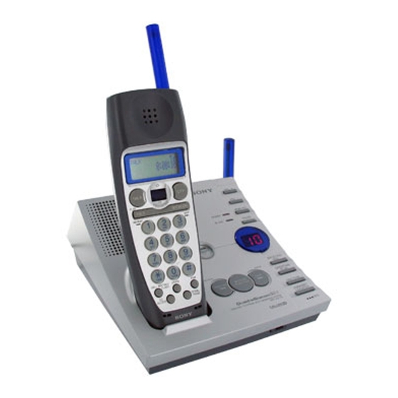
SPP-A2770 SECTION 2 This section is extracted from instruction manual. GENERAL Identifying the parts Refer to the pages indicated in parentheses for details. Base unit 1 CHARGE lamp (p. 14) 6 MESSAGE PLAY/STOP button (p. 60) Lights while the battery is being charged. - Page 6 SPP-A2770 qs Message counter (p. 60, 84) qj MIC (microphone) (p. 52, 65) Indicates the number of new qk Antenna (p. 12) messages recorded. “An” appears ql Hook for AC power adaptor in the announcement only mode. cord (p. 12) “FL”...
- Page 7 SPP-A2770 Identifying the parts (continued) Cordless handset 1 Antenna qf REPEAT . button (p. 61) Press once to repeat the current 2 Speaker message or twice to go back to the 3 Display window (p. 32, 68) previous message. 4 TALK button (p. 32) TONE button (p.
-
Page 8: Registering Additional Cordless Handsets
SPP-A2770 Registering additional cordless handsets The phone system includes a cordless handset. You can expand the system including a total of four cordless handsets. Be sure to register the ID number of the additional cordless handset called “station number” to the base unit before using the additional cordless handset. - Page 9 SPP-A2770 Registering additional cordless handsets (continued) Enter the 10 digits system ID by pressing the dialing keys. The system ID is shown on a sticker affixed to the bottom of the base unit. Press (PGM). You hear a long confirmation beep and the assigned station number is displayed.
-
Page 10: Disassembly
SPP-A2770 SECTION 3 DISASSEMBLY • This set can be disassembled in the order shown below. 3-1. DISASSEMBLY FLOW Cabinet (rear) Hand Main Board Base Cabinet (lower) Assy Base Main Board Note: Follow the disassembly procedure in the numerical order given. -
Page 11: Base Cabinet (Lower) Assy
SPP-A2770 3-4. BASE CABINET (LOWER) ASSY 1 four screws (BTP3 × 10) 5 base cabinet (lower) assy 3 three connectors 4 connector (CN301, 302, 303) (CN172) 3-5. BASE MAIN BOARD 2 four screws (BTP2.6 × 8) 3 BASE MAIN board... -
Page 12: Test Mode
SPP-A2770 SECTION 4 TEST MODE 2. TEST MODE C (TX Power Measurement Mode) BASE UNIT [GREETING REC] In the test mode idling status, press the key to Note: active this mode and display “–C”. The test mode in this set includes the test items that use normal set... - Page 13 SPP-A2770 4. INITIALIZE THE EEPROM [DETAIL OF EACH MODE] In the test mode idling status, EEPROM (IC303) and Flash memory 5. TEST MODE D (RF Control Mode) [ERASE] (IC403) are all cleared except VP setting value when the key is pressed.
- Page 14 SPP-A2770 [VOL--] IF a wrong ID number was entered by mistake, press the 7. TEST MODE B (Writing the ID number) key to return to the test mode idling status, then re-enter correct Note: Though the “TEST MODE E” handles the ID numbers as hexa- ID number.
-
Page 15: Handset
SPP-A2770 Up the jog dial : “UP” is displayed on the second line. HANDSET Down the jog dial : “DN” is displayed on the second line. Press the jog dial : “P” is displayed on the second line. [ENTERING THE TEST MODE] 1. - Page 16 F H-No. : Number of registered handset [PGM] M-No. : Number of model destination (SPP-A2770: 40h) check sum enter 5. TEST MODE B (Writing the ID number) reset Note: Though the “TEST MODE E” handles the ID numbers as hexa- decimal numbers, the “TEST MODE B”...
-
Page 17: Rf Testing
SPP-A2770 Ver 1.1 Test mode setting: RF TESTING – Base Unit – [ERASE] 1. Press three keys of , and simultaneously to This test is for checking the RF system without disassembling the enter the test mode. set in servicing. Perform measurement using the spectrum ana- 2. - Page 18 SPP-A2770 Ver 1.1 REF –10.0 dBm MKR 2.44076 GHz 1-3. TX Power Check 10dB/ A_View Posi B_Blank Norm –14.52 dBm Spectrum analyzer setting: MARKER 2 . 4 4 0 7 6 GHz Center frequency: 2440.5 MHz Span : 10 MHz...
-
Page 19: Electrical Adjustments
SPP-A2770 SECTION 5 ELECTRICAL ADJUSTMENTS C-ID Input Level Measurement 0 dBm = 0.775 V Setting: BASE UNIT • Make the set in the test mode. (See page 12) feeding bridge Base unit Line TP101 Line TP102 Note: The test mode in this set includes the test items that use normal set... - Page 20 SPP-A2770 Between Line and Speaker Signal Level Measure- Between Line and Speaker in The Handset Signal ment Level Measurement Setting: Setting: feeding bridge Base unit feeding bridge Base unit Line TP101 Line TP101 Line TP102 Line TP102 Trunk Trunk 100 µF...
-
Page 21: Handset
SPP-A2770 TX Current Measurement HANDSET Setting: • Make the set in the test mode. (See page 16) Base unit regulated dc power supply Power Failure Test TP201 Procedure: 1. In the test mode idling status, press the key to display +9 V “TEST A”. - Page 22 SPP-A2770 Current Measurement Between Microphone and Speaker (CODEC Loop Setting: Back) Signal Level Measurement (H to H Gain Up) Setting: Same as step 5. Handset regulated dc Procedure: power supply 1. In the step 5 “Between Microphone and Speaker (CODEC TP101 Loop Back) Signal Level Measurement”...
- Page 23 SPP-A2770 Frequency Deviation Measurement Setting: antenna pick-up coil frequency counter – Procedure: 1. Connect equipments as the figure above. 2. In the test mode idling status, press the key to display “TEST C”, and press the keys to set TX on and chan- nel 28.
- Page 24 SPP-A2770 Connecting Location: – BASE MAIN BOARD (Conductor Side) – – BASE MAIN BOARD (Component Side) – TP202 TP201 TP102 TP101 RF271 (RF UNIT) TP472 12 13 (LHS SP GND) R288 R287 TP307 TP474 R285 (LHS MIC GND) TP306 (GND)
-
Page 25: Diagrams
SPP-A2770 SECTION 6 DIAGRAMS 6-1. BLOCK DIAGRAM – BASE UNIT Section – ANT101 (MAIN ANTENNA) ANT102 TEL LINE IC402 (SUB ANTENNA) • SIGNAL PATH B+ SWITCH F101 RF271 Q105 RF UNIT : RX D107 – 110 T101 MJ101 (DL0) L OUT... -
Page 26: Block Diagram - Handset Section
SPP-A2770 6-2. BLOCK DIAGRAM – HANDSET Section – CODEC ANT201 RF61 (ANTENNA) RF UNIT MUTING PCMRO PCMRI VFRO ATTENUATOR AF AMP RXAD PCM L. P. F. EXPANDER CONVERTER ADPCM 8 ANT (SPEAKER) PCMSI PCMSO AIN– MIC AMP MIC1 TXAD PCM B. -
Page 27: Note For Printed Wiring Boards And Schematic Diagrams
SPP-A2770 6-3. NOTE FOR PRINTED WIRING BOARDS AND SCHEMATIC DIAGRAMS • Waveforms – HAND MAIN Board – – BASE MAIN Board – Note on Printed Wiring Board: Note on Schematic Diagram: 1 IC301 tk (CF2) 3 IC1 wl (BCLK) • All capacitors are in µF unless otherwise noted. pF: µµF •... -
Page 28: Printed Wiring Board - Base Main Board (Component Side)
SPP-A2770 6-4. PRINTED WIRING BOARD – BASE MAIN Board (Component Side) – • See page 25 for Note on Printed Wiring Board. • Semiconductor Location Ref. No. Location BASE MAIN BOARD (COMPONENT SIDE) IC203 IC301 IC302 IC402 ANT101 IC403 MAIN... -
Page 29: Printed Wiring Boards - Base Main (Conductor Side)/Base Mic Boards
SPP-A2770 Ver 1.1 6-5. PRINTED WIRING BOARDS – BASE MAIN (Conductor Side)/BASE MIC Boards – • See page 25 for Note on Printed Wiring Board. • Semiconductor Location J201 5 3 1 2 4 6 MJ101 – LINE Ref. No. -
Page 30: Schematic Diagram - Base Main Board (1/3)
SPP-A2770 6-6. SCHEMATIC DIAGRAM – BASE MAIN Board (1/3) – • • See page 25 for Waveform. See page 25 for Note on Schematic Diagram. TP203 R346 R335 R334 4.7k 4.7M R333 C318 R336 R347 C315 100k X301 6MHz CN301... -
Page 31: Schematic Diagram - Base Main (2/3)/Base Mic Boards
SPP-A2770 6-7. SCHEMATIC DIAGRAM – BASE MAIN (2/3)/BASE MIC Boards – • See page 25 for Note on Schematic Diagram. (Page 30) L455 L477 L479 TP475 MIC401 R492 R493 L480 2.2k L456 L478 C497 C500 L475 CN172 TP476 SP401 L476... -
Page 32: Schematic Diagram – Base Main Board (3/3)
SPP-A2770 6-8. SCHEMATIC DIAGRAM – BASE MAIN Board (3/3) – • • See page 25 for Waveform. See page 25 for Note on Schematic Diagram. (Page 30) TP425 C403 C402 R411 R410 C401 L401 2200 60µH TP424 R501 R490 R500... - Page 33 SPP-A2770 • IC Block Diagrams – HAND MAIN Board – ML7079MBZ020 BCLK SYNC AIN – 3 – PCMSO B. P. F. CONVERTER COMPRESSOR NC 4 20kΩ VREF PCMSI NC 6 ADPCM NC 8 PCMRO VFRO PCMRI L. P. F. CONVERTER EXPANDER 20kΩ...
-
Page 34: Printed Wiring Boards - Base Key Board
SPP-A2770 6-9. PRINTED WIRING BOARDS – BASE KEY Board – • See page 25 for Note on Printed Wiring Board. BASE KEY BOARD K722 VOL + K721 VOL – K726 MEMO REC CHARGE IN USE K723 ERASE LED701 (Page 29) -
Page 35: Schematic Diagram - Base Key Board
SPP-A2770 6-10. SCHEMATIC DIAGRAM – BASE KEY Board – • See page 25 for Note on Schematic Diagram. CN702 R710 4.7k TP710 R711 4.7k TP711 R712 4.7k TP712 R713 4.7k TP713 LED701 R714 4.7k TP714 TOD-4201BRN 7 SEGMENTS LED R715 4.7k... -
Page 36: Printed Wiring Board - Hand Main Board
SPP-A2770 6-11. PRINTED WIRING BOARD – HAND MAIN Board – • See page 25 for Note on Printed Wiring Board. HAND MAIN BOARD (COMPONENT SIDE) BZ101 6 54 CHARGE TERMINAL 1 23 TP5 (MIC GND) ANT201 MIC1 1-682-517- (11) D122 – 128 (SPEAKER) D125 –... -
Page 37: Schematic Diagram - Hand Main Board (1/2)
SPP-A2770 6-12. SCHEMATIC DIAGRAM – HAND MAIN Board (1/2) – • • See page 25 for Waveforms. • See page 31 for IC Block Diagrams. See page 25 for Note on Schematic Diagram. RF61 (RF UNIT) 1000 6.3V TP62 ANT201... -
Page 38: Schematic Diagram - Hand Main Board (2/2)
SPP-A2770 6-13. SCHEMATIC DIAGRAM – HAND MAIN Board (2/2) – • • See page 31 for IC Block Diagram. See page 25 for Note on Schematic Diagram. CN121 8.2 nH 8.2 nH 8.2 nH C131 C132 R139 C133 LCD201 C134... -
Page 39: Ic Pin Function Description
SPP-A2770 6-14. IC PIN FUNCTION DESCRIPTION • BASE MAIN BOARD IC301 SB875064W-5W61 (SYSTEM CONTROLLER) Pin No. Pin Name Description SS SPI CLK Serial data transfer clock signal output to the RF unit (RF271) LCD SDA Two-way data bus with the liquid crystal display module Not used (open) LCD CS Chip select signal output to the liquid crystal display module “L”... - Page 40 SPP-A2770 Pin No. Pin Name Description Watch dog timer reset signal input terminal “H”: reset Not used (fixed at “L”) RING DET Detection signal input of the ringer coming “L”: ringer coming Power fail detection signal input “L”: power fail...
- Page 41 SPP-A2770 • BASE MAIN BOARD IC402 DL16561B11BQC (DSP) Description Pin No. Pin Name 7SEG 1F 7 segments LED (LED701) drive signal output 7SEG 1G 7 segments LED (LED701) drive signal output 7SEG 2A 7 segments LED (LED701) drive signal output...
- Page 42 SPP-A2770 Pin No. Pin Name Description VREF Reference voltage output terminal PLLGND — Ground terminal (for internal PLL) PLLVCC — Power supply terminal (+5V) (for internal PLL) VRTC — Power supply terminal (+5V) (for internal real time clock) XOUT System clock output terminal (4.096 MHz) System clock input terminal (4.096 MHz)
- Page 43 SPP-A2770 Pin No. Pin Name Description 7SEG 1C 7 segments LED (LED701) drive signal output 7SEG 1D 7 segments LED (LED701) drive signal output 7SEG 1E 7 segments LED (LED701) drive signal output...
- Page 44 SPP-A2770 • HAND MAIN BOARD IC121 SH875048W-5W62 (SYSTEM CONTROLLER) Pin No. Pin Name Description SS SPI CLK Serial data transfer clock signal output to the RF unit (RF61) LCD SDA Two-way data bus with the liquid crystal display module (LCD201) LCD CS Chip select signal output to the liquid crystal display module (LCD201) “L”...
- Page 45 SPP-A2770 Pin No. Pin Name Description DIS CHG Wakeup control signal output “L” output when discharge (WAKE UP) Watch dog timer reset signal input terminal “H”: reset Not used (fixed at “L”) WAKE UP Wakeup control signal input “H”: wakeup...
-
Page 46: Exploded Views
SPP-A2770 SECTION 7 EXPLODED VIEWS NOTE: • -XX and -X mean standardized parts, so they • Items marked “*” are not stocked since they The components identified by mark 0 or dotted line with mark 0 are may have some difference from the original are seldom required for routine service. -
Page 47: Base Set
SPP-A2770 7-2. BASE SET ANT102 SP401 ANT101 Ref. No. Part No. Description Remark Ref. No. Part No. Description Remark * 51 1-682-653-11 KEY MAIN BOARD * 62 1-682-513-11 BASE MIC BOARD 1-786-172-11 SWITCH, RUBBER KEY (ITAD) 3-910-956-01 HOLDER (MIC) 3-231-531-01 BUTTON (PLAY) -
Page 48: Electrical Parts List
SPP-A2770 BASE KEY SECTION 8 ELECTRICAL PARTS LIST BASE MAIN NOTE: • Due to standardization, replacements in the • Items marked “*” are not stocked since they The components identified by 0 or dotted line with mark mark parts list may be different from the parts speci- are seldom required for routine service. - Page 49 SPP-A2770 BASE MAIN Ref. No. Part No. Description Remark Ref. No. Part No. Description Remark C280 1-162-970-11 CERAMIC CHIP 0.01uF D201 1-216-296-11 SHORT C281 1-162-927-11 CERAMIC CHIP 100PF D202 8-719-991-33 DIODE 1SS133T-77 C282 1-162-908-11 CERAMIC CHIP 0.25PF 50V D203 8-719-991-33 DIODE 1SS133T-77...
- Page 50 SPP-A2770 BASE MAIN Ref. No. Part No. Description Remark Ref. No. Part No. Description Remark R256 1-216-845-11 METAL CHIP 100K 1/16W < MODULAR JACK > R257 1-216-833-11 METAL CHIP 1/16W 0 MJ101 1-794-524-21 JACK, MODULAR (LINE) R259 1-260-089-11 CARBON 1/2W...
- Page 51 SPP-A2770 BASE MAIN BASE MIC HAND MAIN Ref. No. Part No. Description Remark Ref. No. Part No. Description Remark R347 1-216-845-11 METAL CHIP 100K 1/16W R462 1-216-833-11 METAL CHIP 1/16W R356 1-216-819-11 METAL CHIP 1/16W R367 1-216-845-11 METAL CHIP 100K...
- Page 52 SPP-A2770 HAND MAIN Ref. No. Part No. Description Remark Ref. No. Part No. Description Remark < BUZZER > C123 1-115-467-11 CERAMIC CHIP 0.22uF BZ101 1-529-767-11 BUZZER C124 1-109-982-11 CERAMIC CHIP C125 1-126-206-11 ELECT CHIP 100uF 6.3V < CAPACITOR > C126...
- Page 53 SPP-A2770 HAND MAIN Ref. No. Part No. Description Remark Ref. No. Part No. Description Remark 1-414-462-31 INDUCTOR 8.2nH 1-216-835-11 METAL CHIP 1/16W JC10 1-216-864-11 METAL CHIP 1/16W 1-216-864-11 METAL CHIP 1/16W 1-216-857-11 METAL CHIP 1/16W JC12 1-216-296-11 SHORT 1-216-821-11 METAL CHIP...
- Page 54 SPP-A2770 HAND MAIN Ref. No. Part No. Description Remark Ref. No. Part No. Description Remark R117 1-216-833-11 METAL CHIP 1/16W R118 1-216-821-11 METAL CHIP 1/16W < VIBRATOR > R121 1-216-864-11 METAL CHIP 1/16W 1-781-953-21 VIBRATOR, CRYSTAL (10.368MHz) R122 1-216-864-11 METAL CHIP...
- Page 55 SPP-A2770 MEMO...
-
Page 56: Revision History
SPP-A2770 REVISION HISTORY Clicking the version allows you to jump to the revised page. Also, clicking the version at the upper right on the revised page allows you to jump to the next revised page. Ver. Date Description of Revision 2001.08...