Sony NW-HD3 Service Manual
Portable hard disk audio player
Hide thumbs
Also See for NW-HD3:
- Operating instructions manual (458 pages) ,
- Specifications (2 pages) ,
- Operating instructions (2 pages)
Table of Contents
Advertisement
Quick Links
SERVICE MANUAL
Ver. 1.3 2005.02
• SonicStage and SonicStage logo are trademarks
or registered trademarks of Sony Corporation.
• OpenMG, ATRAC3plus and their logos are
trademarks of Sony Corporation.
• Microsoft, Windows, Windows NT and
Windows Media are trademarks or registered
trademarks of Microsoft Corporation in the
United States and/or other countries.
• IBM and PC/AT are registered trademarks of
International Business Machines Corporation.
• Macintosh is a trademark of Apple Computer,
Inc. in the United States and/or other countries.
• Pentium is a trademark or a registered trademark
of Intel Corporation.
• Adobe and Adobe Reader are trademarks or
registered trademarks of Adobe Systems
Incorporated in the United States and/or other
countries.
• US and foreign patents licensed from Dolby
Laboratories.
• All other trademarks and registered trademarks
are trademarks or registered trademarks of their
respective holders.
• In this manual,
TM
and ® marks are not specified.
Sony Corporation
9-879-363-04
Connect Company
2005B05-1
Published by Sony Engineering Corporation
© 2005.02
For other Service and User Manuals, go to www.ManualDepot.com
Maximum recordable number of track
(Approx.)*
ATRAC3
ATRAC3plus
MP3
5,000
2,500
5,000
(132 kbps)
(256 kbps)
(128 kbps)
6,000
10,000
10,000
(105 kbps)
(64 kbps)
(64 kbps)
10,000
13,000
(66 kbps)
(48 kbps)
* When transferring four-minute tracks
Sampling frequency
44.1 kHz (ATRAC3plus), 32/44.1/48 kHz (MP3)
Audio compression technology
Adaptive Transform Acoustic Coding3plus
(ATRAC3plus), MPEG-1 Audio Layer-3 (MP3)
Frequency response
20 to 20,000 Hz
(single signal measurement during playback)
Output
i
(headphones)/LINE OUT* :
Stereo minijack/194 mV
* The jack is used for both headphones and LINE OUT.
Operating temperature
5 to 35°C (41 to 95°F)
Power source
DC IN 6 V (for built-in rechargeable battery)
Battery life (continuous playback)
ATRAC3plus format (48 kbps): Approx. 30 hours
MP3 format (128 kbps): Approx. 22 hours
PORTABLE HARD DISK AUDIO PLAYER
NW-HD3
AEP Model
Australian Model
Chinese Model
Tourist Model
SPECIFICATIONS
Dimension
Not including projecting parts:
90.0 × 62.1 × 14.8 (the thinnest part 13.8) mm
(3 5/8 × 2 1/2 × 19/32 (the thinnest part 9/16)
inches) (w/h/d)
Including projecting parts:
90.8 × 63.4 × 15.7 mm
(3 5/8 × 2 1/2 × 5/8 inches) (w/h/d)
Mass
Approx. 130 g (4.6 oz)
Supplied Accessories
• Headphones (1)
• USB adaptor (1)
(For connecting to the supplied USB cable and the
supplied AC power adaptor)
• Dedicated USB cable (1)
• AC power adaptor (1) (Except E model) *
• Carrying case (1)
• CD-ROM (1) *
2
(SonicStage, PDF of Operating Instructions)
• Quick Start Guide (1)
*
1
For customers in the US
The AC power adaptor supplied with this unit is
not intended to be serviced. Should the AC power
adaptor cease to function in its intended manner
during the warranty period, the adaptor should be
returned to your nearest Sony Service Center or
Sony Authorized Repair Center for replacement,
or if a problem occurs after the warranty period
has expired, the adaptor should be discarded.
2
*
Do not play this CD-ROM on an audio CD player.
Design and specifications are subject to change
without notice.
US Model
UK Model
E Model
1
Advertisement
Table of Contents

Related Manuals for Sony NW-HD3


Summary of Contents for Sony NW-HD3
-
Page 1: Specifications
Operating temperature during the warranty period, the adaptor should be 5 to 35°C (41 to 95°F) returned to your nearest Sony Service Center or Power source Sony Authorized Repair Center for replacement, or if a problem occurs after the warranty period DC IN 6 V (for built-in rechargeable battery) has expired, the adaptor should be discarded. -
Page 2: Table Of Contents
COMPONENTS IDENTIFIED BY MARK 0 OR DOTTED LINE WITH MARK 0 ON THE SCHEMATIC DIAGRAMS AND IN THE PARTS LIST ARE CRITICAL TO SAFE OPERATION. REPLACE THESE COMPONENTS WITH SONY PARTS WHOSE PART NUMBERS APPEAR AS SHOWN IN THIS MANUAL OR IN SUPPLEMENTS PUBLISHED BY SONY. -
Page 3: Servicing Notes
NW-HD3 Ver. 1.3 SECTION 1 SERVICING NOTES System requirements UNLEADED SOLDER Computer IBM PC/AT or Compatible Boards requiring use of unleaded solder are printed with the lead- • CPU: Pentium II 400 MHz or higher (Pentium III 450 MHz or higher is free mark (LF) indicating the solder contains no lead. -
Page 4: General
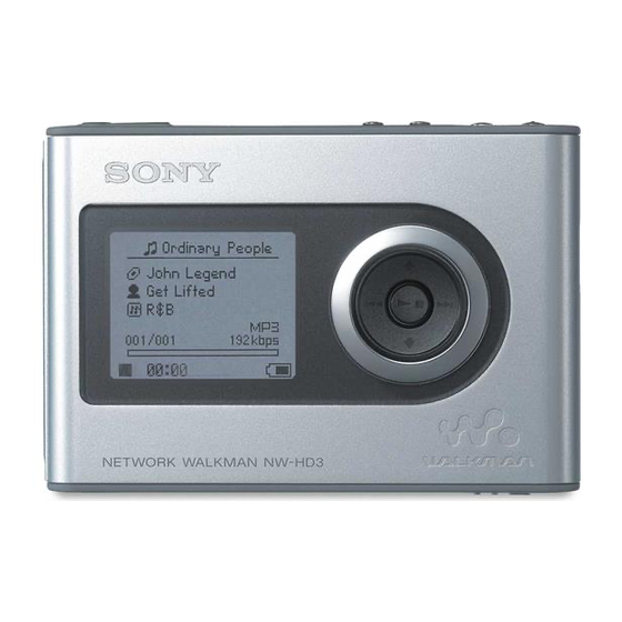
NW-HD3 SECTION 2 This section is extracted from instruction manual. GENERAL Player display Guide to Parts and Controls Player 2 3 4 5 6 7 qj qk w; wa Track number indicator Bookmark indicator Character information display Atrac3plus/MP3 indicator Playback progress bar... -
Page 5: Disassembly
NW-HD3 SECTION 3 DISASSEMBLY • This set can be disassembled in the order shown below. 3-1. DISASSEMBLY FLOW 3-2. CABINET (LOWER) ASSY (Page 5) 3-3. CABINET (MIDDLE) ASSY (Page 6) 3-4. BATTERY BLOCK SUB ASSY (Page 6) 3-5. LCD BLOCK SUB ASSY, MAIN BOARD (Page 7) 3-6. -
Page 6: Cabinet (Middle) Assy
NW-HD3 3-3. CABINET (MIDDLE) ASSY 7 main section 8 cabinet (middle) assy 4 , 6 5 switch unit (O) (CN5002) 2 two screws (M1.4) 3 reinforcement (USB) 1 cover (left) 3-4. BATTERY BLOCK SUB ASSY 3 battery block sub assy 2 toothed lock screw (M1.4) -
Page 7: Lcd Block Sub Assy, Main Board
NW-HD3 3-5. LCD BLOCK SUB ASSY, MAIN BOARD 8 two toothed lock screws (M1.4) 6 flexible board (CN100) 4 sheet (shield HDD) 3 sheet (HDD) 1 toothed lock screw (M1.4) 7 switch unit (H) (CN5003) 2 reinforcement (HPJ) 5 sheet (insulating HDD flexible) 1 toothed lock screw (M1.4) -
Page 8: Hdd Unit
NW-HD3 3-6. HDD UNIT 1 Remove the cabinet (upper) sub assy nine claws in the direction of arrow A . (nine claws) 2 Remove the HDD unit in the direction of arrow B . 3 insulator 5 HDD unit 4 HDD board Note : Extraction and insertion of a HDD board is performed perpendicularly. -
Page 9: Test Mode
NW-HD3 SECTION 4 TEST MODE 1. OUTLINE 5. OPERATION OF THE TEST MODE For the LCD display, the LCD on the main unit is shown, but the 5-1. Power contents of LCD display on the remote commander are same. 5-1-1. Power supply voltage check Operation in the test mode is performed with the main unit. - Page 10 NW-HD3 5. Press the key, “READ” is displayed and hard disk drive 4. Press the , port control state is displayed. In this state, each time [MODE] key is pressed, port control state switch is becomes read state. After 10 seconds, “FIN” is displayed automatically and read performed.
- Page 11 NW-HD3 4. Press the key, “START” is displayed and “1 kHz 0 dBs 7. Press the key, “START” is displayed and “20 kHz 0 dBs L-ch/R-ch VOLUME: 27” audio signal is outputted. In this state, L-ch/R-ch VOLUME: 27” audio signal is outputted.
- Page 12 NW-HD3 7. Press the key, “START” is displayed and “1 kHz 0 dBs 7. Press the key, “START” is displayed and “250 Hz –20 dBs R-ch VOLUME: 27” audio signal is outputted. In this state, L-ch/R-ch VOLUME: 27” audio signal is outputted. In this state, each time [MODE] key is pressed, V-SUR switch is performed.
- Page 13 NW-HD3 5-2-9. Sound pressure regulation level check 5-2-7. Digital sound preset check “1 kHz 0 dBs L-ch/R-ch VOLUME: 30” audio signal is outputted. “100 Hz/10 kHz 0 dBs L-ch/R-ch VOLUME: 27” audio signal is Checking method: outputted. 1. Enter the audio test mode.
- Page 14 NW-HD3 key to display minor item, and press the M m 3. Press the 4. Press the key, X-axis direction is displayed. key to select the “KEY CH”. LCD display LCD display X: *** KEY CH *** : A/D value (hexadecimal) Note: “NG”...
- Page 15 NW-HD3 8. Press the key, monochrome lattice is displayed on the LCD 10. “CALIB” is displayed. Press the key, G-sensor is adjusted. of main unit. Then “FIN”, “DAT NG” or “SEN NG” is displayed automatically. 9. Press the [MENU] key to display minor item, and press the M LCD display m key to select the “LCD 4”.
- Page 16 NW-HD3 Ver. 1.3 5-3-8. Hard disk drive format 5-3-10. Contrast setting This mode is used when performing the format of hard disk drive. Contrast table setting value switch is performed. Checking method: Checking method: 1. Enter the test mode. 1. Enter the test mode.
- Page 17 NW-HD3 5-3-12. Language setting 5. Press the [MENU] key, return to minor item selection screen. Setting the language. 5-3-15. SDRAM check Checking method: 1. Enter the test mode. This mode is used for the check of SDRAM. key to display major item, and press the M m 2.
-
Page 18: Diagrams
NW-HD3 SECTION 5 DIAGRAMS 5-1. BLOCK DIAGRAM – MAIN Section (1/2) – B+ SWITCH Q2001 VDC (MOTOR) HARD DISK VDC (LOGIC) +3.3V_HDD DRIVE UNIT • SIGNAL PATH : AUDIO IC1003 – IC7001 (Page 19) 72 73 74 77 78 83 84 85 81... -
Page 19: Block Diagram - Main Section (2/2)
NW-HD3 Ver. 1.3 5-2. BLOCK DIAGRAM – MAIN Section (2/2) – IC1003 – IC7001 (Page 18) • SIGNAL PATH : AUDIO 186 191 192 193 182 185 183 184 181 88 89 83 HEADPHONE AMP IC4301 D0 – 15 D0 – 15... -
Page 20: Block Diagram - Key/Power Supply Section
NW-HD3 5-3. BLOCK DIAGRAM – KEY/POWER SUPPLY Section – +2.4V_AD (IC1003) +2.4V +2.4V_DAC REGULATOR (IC1003) IC4302 +3.3V (IC4301) +3.3V_HD DC/DC CONVERTER IC9001 +3.3V_A PVIN +3.3V VOUT XSHDN/SS BUFFER Q9002, 9004 MD/SYNC S5009 HOLD PF1/T1 82 SWITCHING +2.8V REGULATOR IC9003 +3.3V... - Page 21 NW-HD3 Ver. 1.3 • Waveform Note on Printed Wiring Board: Note on Schematic Diagram: – MAIN Board – • X : parts extracted from the component side. • All capacitors are in µF unless otherwise noted. (p: pF) • Y : parts extracted from the conductor side.
-
Page 22: Printed Wiring Board - Main Section (1/2)
NW-HD3 Ver. 1.3 :Uses unleaded solder. 5-4. PRINTED WIRING BOARD – MAIN Section (1/2) – MAIN BOARD (COMPONENT SIDE) J4301 /LINE OUT IC1001 SWITCH UNIT IC1002 • Semiconductor FB1005 MENU SP1014 Location MODE , C1001 CN5003 FB4305 VOLUME +/– C4320 + C1025 Ref. -
Page 23: Printed Wiring Board - Main Section (2/2)
NW-HD3 Ver. 1.3 :Uses unleaded solder. 5-5. PRINTED WIRING BOARD – MAIN Section (2/2) – MAIN BOARD (CONDUCTOR SIDE) • Semiconductor TP4312 Location Ref. No. Location D4303 B-10 TP4314 D4304 B-11 TP1008 TP4302 TP4315 TP4308 TP1019 C1018 TP1010 D4303 C1019... -
Page 24: Schematic Diagram - Main Section (1/7)
NW-HD3 • See page 37 for IC Pin Function Description. 5-6. SCHEMATIC DIAGRAM – MAIN Section (1/7) – (1/7) R7009 470k R7010 470k HDD_CNT USB_CNT RMC_DTCK BACKLIGHT_PWR (Page 26) XRESET_LCD XGSEN XGSEN_PWR_CTL XUSLEEP XUSLEEP XURESET R7003 R7004 R7008 XURESET (Page 28) -
Page 25: Schematic Diagram - Main Section (2/7)
NW-HD3 Ver. 1.3 • See page 32 for IC Block Diagram. 5-7. SCHEMATIC DIAGRAM – MAIN Section (2/7) – (2/7) GANDHI_CNT GAND_D GA17 GA17 R1106 FLASH MEMORY FLASH MEMORY IC1102 MBM29SL800BE IC1101 -90PT MBM29SL800BE CSP(Chip Size Package) -90PT (NOT SUPPLIED) -
Page 26: Schematic Diagram - Main Section (3/7)
NW-HD3 • See page 32 for IC Block Diagrams. 5-8. SCHEMATIC DIAGRAM – MAIN Section (3/7) – (3/7) CN5001 DB15 USB_CNT DB14 DB13 XRESET_LCD DB12 BACKLIGHT_PWR (Page 24) DB11 RMC_DTCK DB10 RESET XUCS1 XUWR C5014 XURD 1000p OSC2 R5001 200k... -
Page 27: Schematic Diagram - Main Section (4/7)
NW-HD3 Ver. 1.3 • See page 21 for Waveform. • See page 37 for IC Pin Function Description. 5-9. SCHEMATIC DIAGRAM – MAIN Section (4/7) – (4/7) FS256 GAND_D GAND_A GANDHI_CNT XINTREQH C1010 R1026 TP1007 XINTREQH XINTREQG XINTREQG XINTREQU R1021... -
Page 28: Schematic Diagram - Main Section (5/7)
NW-HD3 • See page 32 for IC Block Diagram. • See page 37 for IC Pin Function Description. 5-10. SCHEMATIC DIAGRAM – MAIN Section (5/7) – (5/7) C8006 C8007 C8005 0.01 6.3V G-SENSOR B+ SWITCH IC8001 IC8000 SN74LVC1G66DCKR HAAM-301BS DZOUT... -
Page 29: Schematic Diagram - Main Section (6/7)
NW-HD3 • See page 21 for Waveform. • See page 32 for IC Block Diagrams. 5-11. SCHEMATIC DIAGRAM – MAIN Section (6/7) – (6/7) CN9501 TP9502 LITHIUM ION BATTERY BATT+ LIS1317HNP BATT- 4.2V 760mAh TP9513 1.8V S9501 2.0V BUILT-IN BATTERY... -
Page 30: Schematic Diagram - Main Section (7/7)
NW-HD3 • See page 21 for Waveform. • See page 32 for IC Block Diagrams. 5-12. SCHEMATIC DIAGRAM – MAIN Section (7/7) – (7/7) 1.2V 1.2V 1.8V 1.8V 3.3V 3.3V (Page 24) XCHG_PG BATT_MON_CTL BATT_MON_CTL PWR_FFCLR PWR_FFCLR C9007 C9012 C9006... -
Page 31: Printed Wiring Board - Hdd Section
NW-HD3 5-13. PRINTED WIRING BOARD – HDD Section – :Uses unleaded solder. 5-14. SCHEMATIC DIAGRAM – HDD Section – HDD BOARD (COMPONENT SIDE) HARD DISK CN100 DRIVE UNIT CN101 RESERVED RESERVED GND(LOGIC) GND(LOGIC) VDC(MOTOR) VDC(MOTOR) CN101 VDC(LOGIC) VDC(LOGIC) GND(MOTOR) GND(MOTOR) - Page 32 NW-HD3 Ver. 1.3 • IC Block Diagrams – MAIN Board – IC5001 SM8142BD-G-EL IC3001 CXR710160-211GH IC4301 AN17020A-VB 64 63 62 61 60 59 58 57 56 55 52 51 50 49 PE3/RxD1 HIGH VOLTAGE PE2/TxD1 BEEP SWITCHING CIRCUIT PE1/RxD0 MUTING...
- Page 33 NW-HD3 IC9001 LTC3441EDE#TR SHUTDOWN SHDN/SS SUPPLY CURRENT 1.22V LIMIT COMPARATORS EEEOR LOGIC 2.4V OUTPUT INTERNAL PHASING UVLO AVERAGE CURRENT THERMAL PGND LIMIT SHUTDOWN 3.2A REVERSE CURRENT LIMIT –0.8A PVIN 8 VOUT GATE DRIVERS ANTICTOSS CONDUCTION 1MHz PGND SYNC BURST MODE...
- Page 34 NW-HD3 IC9002 SC901584EPR2 36 35 RESET 2 SERIAL RST2 PASS POWER STEP REGULATOR 3 SWITCH 2 UP-DOWN REGC2 DRIVER RST2 MUTING REG2G REF2 SERIAL VREF BUFFER REGO2 PASS REGULATOR 2 REGI2 32 DTC2 REGC1 VREF RST1 SERIAL REF2 REGO1 PASS...
- Page 35 NW-HD3 IC9003 TPS62200DBVR VI 1 UNDERVOLTAGE LOCKOUT CURRENT LIMIT BIAS SUPPLY COMPARATOR SKIP COMPARATOR SOFT START 1 MHz OSCILLATOR V (COMP) COMPARATOR SAWTOOTH DRIVER GENERATOR CONTROL SHOOT-THROUGH LIGIC LOGIC LOAD COMPARATOR GND 2 COMPENSATION EN 3 VREF=0.5V IC9501 BQ24010ADRCR IN 1...
- Page 36 NW-HD3 IC9503 R2061K01-E2 9 /INTR LEVEL SIO 1 SHIFTER SCLK 2 8 OSCOUT REAL TIME VOLTAGE CLOCK REFERENCE /VDCC 3 7 OSCIN DELAY BATTERY VOLTAGE MONITOR VOLTAGE DETECTOR IC9504 TPS2113APWR INTERNAL 1µA THERMAL ULVO SENSE STAT 1 ULVO CONTROL ULVO...
- Page 37 NW-HD3 • IC Pin Function Description MAIN BOARD IC1003 CXR704060-201GA (SYSTEM CONTROLLER, D/A CONVERTER) Pin No. Pin Name Description VDIO0 — Power supply terminal (+1.8V) (for I/O interface) PM4/A12 to PM7/A15, 2 to 10 Address signal output to the flash memory and multi interface...
- Page 38 NW-HD3 Pin No. Pin Name Description PE3/RXD1 Data input terminal Not used PE4/SCK1 Serial clock signal output to the power control and real time clock PE5/SO1 Serial data output to the power control and real time clock PE6/SI1 Serial data input from the real time clock...
- Page 39 NW-HD3 Pin No. Pin Name Description PD2/DPLS Test terminal for debug Not used PD3/DMNS Test terminal for debug Not used PD4/TXDPLS Test terminal for debug Not used PD5/TXDMNS Test terminal for debug Not used PD6/TXENL Test terminal for debug Not used...
- Page 40 NW-HD3 Ver. 1.3 Pin No. Pin Name Description MSINS Card detection signal input from the memory stick interface Not used HOLD key detection signal input terminal “L”: hold P10/DADT Audio data input from the memory stick interface Not used P11/ADDT...
- Page 41 NW-HD3 MAIN BOARD IC2001 1S1R72003BOOA100 (USB CONTROLLER) Pin No. Pin Name Description Internal operation setting terminal N.C. — Not used AVSS — Ground terminal (analog system) AVDD — Power supply terminal (+3.3V) (analog system) AVSS — Ground terminal (analog system) AVDD —...
- Page 42 NW-HD3 Pin No. Pin Name Description HIORDY Wait signal input from the hard disk drive unit — Ground terminal (logic system) — Power supply terminal (+3.3V) (logic system) XHDMACK DMA acknowledge signal output to the hard disk drive unit HINTRQ...
- Page 43 NW-HD3 MAIN BOARD IC7001 CXD1616GH (MULTI INTERFACE) Pin No. Pin Name Description XTAL Sub system clock input terminal Not used EXTAL Sub system clock output terminal Not used CLK2550A Clock signal (22.5792 MHz) output to the sub system controller CLK2550X Clock signal (22.5792 MHz) inversion output to the sub system controller...
- Page 44 NW-HD3 Pin No. Pin Name Description HIORDY Wait signal input from the hard disk drive unit XHDMACK DMA acknowledge signal output to the hard disk drive unit HDMARQ DMA request signal input from the hard disk drive unit HINTREQ Interrupt request signal input from the hard disk drive unit...
-
Page 45: Exploded View
NW-HD3 Ver. 1.3 SECTION 6 EXPLODED VIEWS NOTE: • -XX and -X mean standardized parts, so they • Items marked “*” are not stocked since they may have some difference from the original are seldom required for routine service. Some one. -
Page 46: Main Section
NW-HD3 Ver. 1.3 6-2. MAIN SECTION not supplied not supplied MAIN board Ref. No. Part No. Description Remark Ref. No. Part No. Description Remark A-1104-130-A HDD BOARD, COMPLETE X-2050-782-1 MAIN BOARD, COMPLETE (for service) 2-148-885-01 SHEET (INSULATING HDD FLEXIBLE) (US, MX, AUS) -
Page 47: Electrical Parts List
NW-HD3 Ver. 1.3 SECTION 7 MAIN ELECTRICAL PARTS LIST NOTE: The components identified by mark • Due to standardization, replacements in the • Items marked “*” are not stocked since they 0 or dotted line with mark 0 are parts list may be different from the parts are seldom required for routine service. - Page 48 NW-HD3 MAIN Ref. No. Part No. Description Remark Ref. No. Part No. Description Remark C7003 1-100-504-11 CERAMIC CHIP 0.1uF 6.3V C3012 1-100-504-11 CERAMIC CHIP 0.1uF 6.3V C7004 1-100-504-11 CERAMIC CHIP 0.1uF 6.3V C3013 1-100-506-11 CERAMIC CHIP 6.3V C7005 1-100-504-11 CERAMIC CHIP 0.1uF...
- Page 49 NW-HD3 Ver. 1.3 MAIN Ref. No. Part No. Description Remark Ref. No. Part No. Description Remark FB1005 1-469-082-21 INDUCTOR, FERRITE BEAD (1005) C9039 1-128-613-91 CERAMIC CHIP 47PF C9040 1-128-613-91 CERAMIC CHIP 47PF FB1011 1-469-082-21 INDUCTOR, FERRITE BEAD (1005) C9501 1-165-908-11 CERAMIC CHIP...
- Page 50 NW-HD3 Ver. 1.3 MAIN Ref. No. Part No. Description Remark Ref. No. Part No. Description Remark * L9003 1-400-581-11 INDUCTOR 220uH R2003 1-469-084-21 FERRITE L9004 1-400-810-11 INDUCTOR 4.7uH R2004 1-218-977-11 RES-CHIP 100K 1/16W L9005 1-456-274-21 INDUCTOR 10uH R2005 1-208-905-11 METAL CHIP 5.6K...
- Page 51 NW-HD3 MAIN Ref. No. Part No. Description Remark Ref. No. Part No. Description Remark R3025 1-218-990-11 SHORT CHIP R7012 1-218-933-11 RES-CHIP 1/16W R3026 1-218-990-11 SHORT CHIP R8001 1-218-985-11 RES-CHIP 470K 1/16W R8002 1-218-929-11 RES-CHIP 1/16W R3027 1-218-990-11 SHORT CHIP R8005...
- Page 52 NW-HD3 Ver. 1.3 MAIN Ref. No. Part No. Description Remark Ref. No. Part No. Description Remark R9514 1-218-990-11 SHORT CHIP ACCESSORIES R9515 1-218-990-11 SHORT CHIP ************ R9516 1-218-990-11 SHORT CHIP 1-478-393-11 ADAPTOR, AC (AC-ES608K) (US, MX, TW) R9517 1-218-990-11 SHORT CHIP...
- Page 53 NW-HD3 MEMO...
-
Page 54: Revision History
NW-HD3 REVISION HISTORY Clicking the version allows you to jump to the revised page. Also, clicking the version at the upper right on the revised page allows you to jump to the next revised page. Ver. Date Description of Revision 2004.12...