Table of Contents
Advertisement
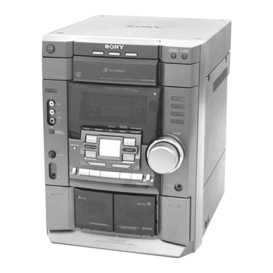
SERVICE MANUAL
Ver 1.1 2001.11
• HCD-DX80 is the tuner, deck, CD and
amplifier section in MHC-DX80.
Sony Corporation
9-929-593-12
2001K0500-1
Home Audio Company
C 2001.11
Published by Sony Engineering Corporation
HCD-DX80
Model Name Using Similar Mechanism
CD
CD Mechanism Type
Section
Base Unit Name
Optical Pick-up Name
Tape deck
Model Name Using Similar Mechanism
Section
Tape Transport Mechanism Type
SPECIFICATIONS
MINI HI-FI COMPONENT SYSTEM
E Model
HCD-DX50
CDM58E-30BD60
BU-30BD60
A-MAX.3
NEW
TCM-230AWR41
– Continued on next page –
Advertisement
Table of Contents

Related Manuals for Sony HCD-DX80


Summary of Contents for Sony HCD-DX80
- Page 1 HCD-DX80 SERVICE MANUAL E Model Ver 1.1 2001.11 • HCD-DX80 is the tuner, deck, CD and amplifier section in MHC-DX80. Model Name Using Similar Mechanism HCD-DX50 CD Mechanism Type CDM58E-30BD60 Section Base Unit Name BU-30BD60 Optical Pick-up Name A-MAX.3 Tape deck...
- Page 2 LINE WITH MARK 0 ON THE SCHEMATIC DIAGRAMS AND IN THE PARTS LIST ARE CRITICAL TO SAFE OPERATION. REPLACE THESE COMPONENTS WITH SONY PARTS WHOSE PART NUMBERS APPEAR AS SHOWN IN THIS MANUAL OR IN SUPPLEMENTS PUB- LISHED BY SONY.
-
Page 3: Table Of Contents
HCD-DX80 TABLE OF CONTENTS MODEL IDENTIFICATION — BACK PANEL — GENERAL ..............4 DISASSEMBLY ............7 2-1. Disassembly Flow ............7 2-2. Case (Top) ............... 8 2-3. Loading Panel ..............8 2-4. CD Mechanism Deck (CDM58E-30BD60) ....9 2-5. Front Panel Section ............9 2-6. -
Page 4: General
HCD-DX80 SECTION 1 This section is extracted from instruction manual. GENERAL... - Page 5 HCD-DX80...
- Page 6 HCD-DX80...
-
Page 7: Disassembly
HCD-DX80 SECTION 2 DISASSEMBLY • This set can be disassembled in the order shown below. 2-1. DISASSEMBLY FLOW 2-2. CASE (TOP) (Page 8) 2-3. LOADING PANEL (Page 8) 2-4. CD MECHANISM DECK (CDM58E-30BD60) (Page 9) 2-5. FRONT PANEL SECTION 2-10. BASE UNIT (BU-30BD60) -
Page 8: Case (Top)
HCD-DX80 Note: Follow the disassembly procedure in the numerical order given. 2-2. CASE (TOP) case (Top) 5 two screws (case 3 TP2) 9 four screws (+BVTP 3 × 12) 7 two screws (+BVTP 3 × 10) 8 side panel (L) -
Page 9: Cd Mechanism Deck (Cdm58E-30Bd60)
HCD-DX80 2-4. CD MECHANISM DECK (CDM58E-30BD60) CD mechanism deck (CDM58E-30BD60) wire (flat type) (21 core) (CN201) connector CN202) 4 screw (+BVTP 3 × 10) screw (+BVTP 3 × 10 2-5. FRONT PANEL SECTION connector ( CN607) wire (flat type) (17 core) -
Page 10: Tape Mechanism Deck (Tcm-230Awr41)
HCD-DX80 2-6. TAPE MECHANISM DECK (TCM-230AWR41) 1 five screws (+BVTP 2.6 × 8) 2 Tape mechanism deck (TCM-230AWR41) 2-7. BACK PANEL SECTION back panel section 4 five screws (+BVTP 3 × 10) connector (CN505) 5 two screws (+BVTP 3 × 10) -
Page 11: Main Board
HCD-DX80 2-8. MAIN BOARD MAIN board 2 MAIN board 1 two screws (+BVTP 3 × 10) 2-9. LEAF SW BOARD, HEAD (A) BOARD, HEAD (B) BOARD 2 five claws 3 LEAF SW board 1 Remove the four solderings. 5 head (A) board 7 head (B) board 4 screw (+PTT 2 ×... -
Page 12: Base Unit (Bu-30Bd60)
HCD-DX80 2-10. BASE UNIT (BU-30BD60) 1 screw (+PTPWH M2.6) 2 holder assy base unit qs two insulators (BU-30) (BU-30BD60) q; screws (DIA. 12) qs two insulators (BU-30) 9 two screws (+PTPWH M2.6) 8 two stoppers (BU) 7 two screws (+BVTP 2.6 × 8) -
Page 13: Test Mode
HCD-DX80 SECTION 3 TEST MODE [Cold Reset] 7. In the key check mode, the fluorescent indicator tube displays • The cold reset clears all data including preset data stored in the “K0 V0”. Each time a button is pressed, “KEY” value increases. - Page 14 HCD-DX80 * Tape function [CD Ship Mode (Memory Clear) ] 1. When a tape is inserted in Deck B and recording is started, the • This mode moves the pickup to the position durable to vibra- input source function selects VIDEO automatically.
-
Page 15: Mechanical Adjustments
HCD-DX80 SECTION 4 SECTION 5 MECHANICAL ADJUSTMENTS ELECTRICAL ADJUSTMENTS Precaution DECK SECTION 0 dB=0.775 V 1. Clean the following parts with a denatured alcohol-moistened swab: 1. Demagnetize the record/playback head with a head record/playback heads pinch rollers demagnetizer. erase head rubber belts 2. - Page 16 HCD-DX80 2. Turn the adjustment screw and check output peaks. If the peaks DECK B Tape Speed Adjustment do not match for L-CH and R-CH, turn the adjustment screw Note: Start the Tape Speed adjustment as below after setting to the test so that outputs match within 1dB of peak.
- Page 17 HCD-DX80 DECK B REC Bias Adjustment 4. Mode: Record Procedure: In the MC test mode, the “REC memory mode” is convenient for MD/VIDEO (AUDIO) IN (J101) this adjustment. In the “REC memory mode” , when the REC starts 315 Hz, 50 mV (–23.8 dB) AF OSC the input signal FUNCTION is switched to VIDEO automatically.
- Page 18 HCD-DX80 TUNER SECTION CD SECTION FM Tuned Level Adjustment Note : 1. CD Block is basically designed to operate without adjustment. FM RF SIGNAL GENERATOR Therefore, check each item in order given. 2. Use LUV-P01 (4-999-032-01) unless otherwise indicated. 75 Ω coaxial 3.
- Page 19 HCD-DX80 Note : Clear RF signal waveform means that the shape “ ◊ ” can be clearly Adjustment Location: distinguished at the center of the waveform. [BD BOARD] (Conductor Side) RF signal waveform VOLT/DIV : 200mV TIME/DIV : 500ns level : 0.65 ± 0.15Vp-p (RFDC) 1.1 ±...
- Page 20 HCD-DX80 MEMO...
-
Page 21: Diagrams
HCD-DX80 SECTION 6 DIAGRAMS 6-1. BLOCK DIAGRAM – TUNER/CD Section – AM/FM IF AMP, MPX FM FRONT-END LPF11 IC11 RF IF BUFFER L-CH • R-CH is omitted due to same as L-CH. ANT IN IF OUT FM IF L OUT •... -
Page 22: Block Diagram -Main Section
HCD-DX80 6-2. BLOCK DIAGRAM – MAIN Section – INPUT SELECT G EQ IC101 IC102 IC501 TM801 (Page 21) L-CH IN2A VOL OUT2 SPEAKER POWER Q504,505 Q861 Q821,822 IC106 IMPEDANCE RY801 LOUT Q824,825 (Page 21) R CH USE 6~16Ω MUTING MUTING... -
Page 23: Singapore Model
HCD-DX80 6-3. NOTE FOR PRINTED WIRING BOARDS AND SCHEMATIC DIAGRAMS (In addition to this, the necessary note is printed in each block) Note on Printed Wiring Boards: Note on Schematic Diagram: • Circuit Boards Location • All capacitors are in µF unless otherwise noted. pF: µµF •... -
Page 24: Schematic Diagram -Bd Board
HCD-DX80 6-4. SCHEMATIC DIAGRAM – BD Board – • See page 31 for Waveforms • See page 44 for IC Block Diagrams. IC B/D IC B/D IC B/D (Page 27) -
Page 25: Printed Wiring Board -Bd Board
HCD-DX80 6-5. PRINTED WIRING BOARD – BD Board – • See page 23 for Circuit Boards Location. • Semiconductor Location (Page 30) Ref. No. Location D101 IC101 IC102 IC103 Q101 Q102 There are a few cases that the part printed on... -
Page 26: Schematic Diagram -Main Board (1/4)
HCD-DX80 6-6. SCHEMATIC DIAGRAM – MAIN Board (1/4) – • See page 31 for Wavefoms. • See page 44 for IC Block Diagram. • Voltages and waveforms are dc with respect to ground under no-signal (detuned) conditions. • no mark : FM... -
Page 27: Schematic Diagram -Main Board (2/4)
HCD-DX80 6-7. SCHEMATIC DIAGRAM – MAIN Board (2/4) – • Voltages are dc with respect to ground under no-signal (detuned) conditions. no mark : FM ) : TAPE ] : CD (Page 24) (Page 26) (Page 40) (Page 29) (Page 28) -
Page 28: Schematic Diagram -Main(3/4)/Head Board
HCD-DX80 6-8. SCHEMATIC DIAGRAM – MAIN (3/4)/HEAD Board – • See page 31 for Waveform. • See page 44 for IC Block Diagrams. • See page 39 for Printed Wiring Board of Head Boards. (Page 27) (Page 29) • Voltages and waveforms are dc with respect to ground The components identified by mark 0 or dotted under no-signal (detuned) conditions. -
Page 29: Schematic Diagram -Main Board (4/4)
HCD-DX80 6-9. SCHEMATIC DIAGRAM – MAIN Board (4/4) – • See page 31 for Waveforms. • See page 47 for IC Pin Function Description. (Page 32) (Page 32) (Page (Page • Voltages and waveforms are dc with respect to ground under no-signal (detuned) conditions. -
Page 30: Printed Wiring Board -Main Board
HCD-DX80 6-10. PRINTED WIRING BOARD – MAIN Board – • See page 23 for Circuit Boards Location. • Semiconductor Location (Page 41) DRIVER BOARD BD BOARD (Page 25) Ref. No. Location Ref. No. Location CN701 CN101 MAIN BOARD A-12 IC701... - Page 31 HCD-DX80 MEMO • Waveforms – BD Board – – MAIN Board – – PANEL Board – 1 IC101 ta (RFAC) (CD Play mode) 1 IC51 ws TUNER (FM) 6 IC601 is (X OUT) (Stop mode) 1.1 Vp-p 4.3 Vp-p 3.5 Vp-p 4.5 MHz...
-
Page 32: Schematic Diagram -Power Amp/Sensor Board
HCD-DX80 6-11. SCHEMATIC DIAGRAM – POWER AMP/SENSOR Board – (Page 42) (Page 29) (Page 42) (Page 29) The components identified by mark 0 or dotted line with mark 0 are critical for safety. Replace only with part number specified. • Voltages are dc with respect to ground under no-signal (detuned) conditions. -
Page 33: Printed Wiring Boards -Power Amp/Sensor Board
HCD-DX80 6-12. PRINTED WIRING BOARDS – POWER AMP/SENSOR Board – • See page 23 for Circuit Boards Location. • Semiconductor Location (CHASSIS) POWER AMPLIFIER BOARD Ref. No. Location D501 D502 D503 D504 D541 D543 D551 D581 D941 IC501 Q501 Q503... -
Page 34: Schematic Diagram -Panel/Video Switch Board
HCD-DX80 6-13. SCHEMATIC DIAGRAM – PANEL/VIDEO SWITCH Board – • See page 31 for Waveform. • See page 47 for IC Pin Function Description. • See page 44 for IC Block Diagram. (Page 36) (Page 29) (Page 36) • Voltages and waveforms are dc with respect to ground under no-signal (detuned) conditions. -
Page 35: Printed Wiring Boards -Panel/Video Switch Board
HCD-DX80 6-14. PRINTED WIRING BOARDS – PANEL/VIDEO SWITCH Board – • See page 23 for Circuit Boards Location. (Page 37) • Semiconductor PANEL BOARD CD-SW BOARD Location NO603 Ref. No. Location D608 A-10 D609 D608, S605 D613, 614 D610 GAME... -
Page 36: Schematic Diagram -Cd Switch/Pad Switch Board
HCD-DX80 6-15. SCHEMATIC DIAGRAM – CD SWITCH/PAD SWITCH Board – (Page 34) • Voltages are dc with respect to ground under no-signal (detuned) conditions. no mark : FM (Page 34) -
Page 37: Printed Wiring Boards -Cd Switch/Pad Switch Board
HCD-DX80 • See page 23 for Circuit Boards Location. 6-16. PRINTED WIRING BOARDS – CD SWITCH/PAD SWITCH Board – CD-SW BOARD D794, S796 1-680-263- D793, S793 D791, S795 D792, S794 S791 – 796 DISC 3 DISC 2 DISC 1 OPEN... -
Page 38: Schematic Diagram -Leaf Sw Board
HCD-DX80 6-17. SCHEMATIC DIAGRAM –LEAF SW Board – (Page 29) • Voltages are dc with respect to ground under no-signal There are a few cases that the part printed on conditions. this diagram isn’t mounted in this model. no mark : TAPE PLAY... -
Page 39: Printed Wiring Boards -Leaf Sw/Head Board
HCD-DX80 6-18. PRINTED WIRING BOARDS – LEAF SW/HEAD Board – • See page 23 for Circuit Boards Location. • See page 28 for Schematic Diagram of Head Board. • Semiconductor PM902 Location Ref. No. Location PM901 D1001 IC1002 D1002 B-10... -
Page 40: Schematic Diagram -Address Sensor/Driver/Motor Board
HCD-DX80 6-19. SCHEMATIC DIAGRAM – ADDRESS SENSOR/DRIVER/MOTOR Board – • See page 44 for IC Block Diagram. IC B/D (2/4) (Page 27) • Voltages are dc with respect to ground under no-signal (detuned) conditions. no mark : CD STOP... -
Page 41: Printed Wiring Boards -Address Sensor/Driver/5Motor Board
HCD-DX80 6-20. PRINTED WIRING BOARDS – ADDRESS SENSOR/DRIVER/MOTOR Board – • See page 23 for Circuit Boards Location. • Semiconductor Location Ref. No. Location D701 IC701 IC711 C712 IC711 (14) (14) There are a few cases that the part printed on this diagram isn’t mounted in this model. -
Page 42: Schematic Diagram -Main Trans/Sub Trans Board
HCD-DX80 6-21. SCHEMATIC DIAGRAM – MAIN TRANS/SUB TRANS Board – The components identified by mark 0 or dotted line with mark 0 are critical for safety. Replace only with part number specified. • Voltages are dc with respect to ground under no-signal (detuned) conditions. -
Page 43: Printed Wiring Boards -Main Trans/Sub Trans Board
HCD-DX80 6-22. PRINTED WIRING BOARDS – MAIN TRANS/SUB TRANS Board – • See page 23 for Circuit Boards Location. • Semiconductor AC IN Location MAIN TRANS BOARD SUB TRANS BOARD Ref. No. Location D971 (EXCEPT MX) D972 D973 (EXCEPT MX) - Page 44 HCD-DX80 • IC Block Diagrams – BD Board – IC101 CXD3017Q IC103 CXA2581N-T4 RW/ROM 59 58 57 46 45 44 DC OFST Digital RFDCI – – RFDCO LRCK OP Amp PCMD Interface Digital Asymmetry Converter Analog SW Corrector XTSL –...
- Page 45 HCD-DX80 – MAIN Board – IC11 LA1845 PF.AMP DEOODER PILOT BUFF ANTI-BIRDIE CANCEL P-DET STEREO ø LEVEL AM/FM COMP S-CURVE BUFF PILOT π 304kHz 19k 0 TUNING DRIVE IC51 LC72131 PHASE DETECTOR CHARGE PUMP POWER REFERENCE UNLOCK DIVIDER DETECTOR RESET...
-
Page 46: Panel Board
HCD-DX80 – PANEL Board – – DRIVER Board – IC602 BA3830F-E2 IC701 BA6956AN REFFERENCE RESET 18 RESET CURRENT REFFERENCE 17 f01 CURRENT CONTROL LOGIC LINE 16 f02 LINE 15 f03 13 f05 RESET 12 f06 BIAS 11 REC Bias LEVEL... -
Page 47: Ic Pin Function Description
HCD-DX80 6-23. IC PIN FUNCTION DESCRIPTION • MAIN BOARD IC501 M30620MCA-A95FP (SYSTEM CONTROLLER) Pin No. Pin Name Description AUDIO OUT Audio output signal on/off control “H”: ON, “L”: OFF Not used (open) ON/OFF STEREO Stereo detection signal input from the LA1845 (IC11) “L”: Stereo in TUNED Tuning detection signal input from the LA1845 (IC11) “L”: Tuned in... - Page 48 HCD-DX80 Pin No. Pin Name Description LOAD-OUT Turn motor control signal output to the BA6956AN (IC701) OPEN-SW Tray open detect signal input terminal “L”: open CLOSE-SW Tray close detect signal input terminal “L”: close BU UP/DOWN- Pick-up up/down detect signal input terminal...
- Page 49 HCD-DX80 Pin No. Pin Name Description STBY-RELAY Standby relay on/off control signal output to the RY971 “H”: relay on REAR-RELAY Rear speaker relay on/off control signal output to the STA. AMP (TA-DX80) “H”: relay on SURR-RELAY Surround speaker relay on/off control signal output terminal “H”: relay on Not used (open) FRONT-RELAY Front speaker relay on/off control signal output to the RY801 “H”: relay on...
- Page 50 HCD-DX80 • PANEL BOARD IC601 MB90M407PF-G-103-BND (DISPLAY CONTROL) Pin No. Pin Name Description 1 to 5 G5 to G1 FL grid drive signal output 6 to 10 P1 to P5 FL segment drive signal output VSS IO — Ground terminal (VSS for I/O)
- Page 51 HCD-DX80 Pin No. Pin Name Description XOUT System clock output terminal (4MHz) System clock input terminal (4MHz) VCC-CPU — Power supply terminal (+3.3V) (VCC for CPU) 85 to 91 NO USE Not used (open) SOFT TEST Soft test terminal Not used (open)
-
Page 52: Exploded Views
HCD-DX80 SECTION 7 EXPLODED VIEWS NOTE: • -XX and -X mean standardized parts, so they • Items marked “*” are not stocked since they The components identified by mark 0 or dotted line with mark may have some difference from the original are seldom required for routine service. -
Page 53: Front Panel Section
HCD-DX80 7-2. FRONT PANEL SECTION not supplied not supplied TCM-230AWR41 not supplied not supplied Ref. No. Part No. Description Remark Ref. No. Part No. Description Remark A-2004-868-A HOLDER (L) ASSY, TC (BR) 4-231-841-01 SPRING (HEART CAM-B) X-4953-360-1 CASSETTE HOLDER (L) ASSY (EXCEPT BR) -
Page 54: Main Board Section
HCD-DX80 7-3. MAIN BOARD SECTION T910 not supplied not supplied The components identified by mark 0 or dotted line with mark 0 are critical for safety. Replace only with part number specified. Ref. No. Part No. Description Remark Ref. No. -
Page 55: Cd Mechanism Deck Section (Cdm58E-30Bd60)
HCD-DX80 Ver 1.1 7-4. CD MECHANISM DECK SECTION (CDM58E-30BD60) M721 BU-30BD60 Ref. No. Part No. Description Remark Ref. No. Part No. Description Remark 4-933-134-11 SCREW (+PTPWH M2.6X8) 4-228-414-01 BRACKET (YOKE) 4-221-679-01 CAM (RELAY) X-4953-307-1 PULLEY (A) ASSY, CHUCKING 4-231-452-01 TABLE (NEW) -
Page 56: Base Unit Section (Bu-30Bd60)
HCD-DX80 7-5. BASE UNIT SECTION (BU-30BD60) not supplied not supplied not supplied The components identified by mark 0 or dotted line with mark 0 are critical for safety. Replace only with part number specified. Ref. No. Part No. Description Remark Ref. -
Page 57: Tape Mechanism Deck Section-1 (Tcm-230Awr41)
HCD-DX80 7-6. TAPE MECHANISM DECK SECTION-1 (TCM-230AWR41) Note: Two different types of tape mechanism are used depending on models. They maintain compatibility as an entire mechanism even though there are some different parts are used. PM901 HP901 PM902 HRPE901 Ref. No. -
Page 58: Tape Mechanism Deck Section-2 (Tcm-230Awr41)
HCD-DX80 7-7. TAPE MECHANISM DECK SECTION-2 (TCM-230AWR41) not supplied not supplied M901 not supplied Ref. No. Part No. Description Remark Ref. No. Part No. Description Remark 3-041-946-01 BELT (CAPSTAN B) 3-318-203-62 SCREW (B1.7X4), TAPPING 4-227-239-01 BELT (CAPSTAN C) 3-019-208-01 WASHER, STOPPER... -
Page 59: Electrical Parts List
HCD-DX80 SECTION 8 ADDRESS SENSOR ELECTRICAL PARTS LIST NOTE: • Due to standardization, replacements in the • COILS The components identified by uH: µH mark 0 or dotted line with mark parts list may be different from the parts speci- 0 are critical for safety. - Page 60 HCD-DX80 CD-SW Ref. No. Part No. Description Remark Ref. No. Part No. Description Remark R181 1-216-081-00 METAL CHIP 1/10W < IC > R182 1-216-081-00 METAL CHIP 1/10W R183 1-216-081-00 METAL CHIP 1/10W IC101 8-752-402-31 IC CXD3017Q R190 1-216-033-00 METAL CHIP...
- Page 61 HCD-DX80 DRIVER HEAD (A) HEAD (B) LEAF SW MAIN Ref. No. Part No. Description Remark Ref. No. Part No. Description Remark 1-675-912-14 DRIVER BOARD < RESISTOR > ************* R907 1-247-879-11 CARBON 100K 1/4W < CAPACITOR > R1001 1-249-409-11 CARBON 1/4W...
- Page 62 HCD-DX80 MAIN Ref. No. Part No. Description Remark Ref. No. Part No. Description Remark 1-126-963-11 ELECT 4.7uF C135 1-126-964-11 ELECT 10uF 1-162-974-11 CERAMIC CHIP 0.01uF C136 1-126-964-11 ELECT 10uF C137 1-126-964-11 ELECT 10uF 1-126-962-11 ELECT 3.3uF C139 1-126-935-11 ELECT 470uF 1-162-974-11 CERAMIC CHIP 0.01uF...
- Page 63 HCD-DX80 MAIN Ref. No. Part No. Description Remark Ref. No. Part No. Description Remark C312 1-126-959-11 ELECT 0.47uF C382 1-137-427-11 MYLAR 120PF C313 1-162-964-11 CERAMIC CHIP 0.001uF C383 1-162-961-11 CERAMIC CHIP 330PF C384 1-162-946-11 CERAMIC CHIP 27PF C314 1-126-964-11 ELECT...
- Page 64 HCD-DX80 MAIN Ref. No. Part No. Description Remark Ref. No. Part No. Description Remark 1-760-023-11 FILTER, CERAMIC < FRONT END > < CONNECTOR > 1-693-477-12 FRONT END (3 GANGS) (FM FRONT-END) * CN101 1-565-291-11 SOCKET, CONNECTOR 13P < IC >...
- Page 65 HCD-DX80 MAIN Ref. No. Part No. Description Remark Ref. No. Part No. Description Remark Q829 8-729-120-28 TRANSISTOR 2SC1623-T1-L5L6 JR38 1-216-864-11 SHORT JR104 1-216-864-11 SHORT Q831 8-729-113-69 TRANSISTOR FN1F4M-T1M32 JR201 1-216-864-11 SHORT Q832 8-729-120-28 TRANSISTOR 2SC1623-T1-L5L6 JR301 1-216-864-11 SHORT Q861 8-729-113-69 TRANSISTOR...
- Page 66 HCD-DX80 MAIN Ref. No. Part No. Description Remark Ref. No. Part No. Description Remark 1-216-829-11 METAL CHIP 4.7K 1/16W R163 1-216-825-11 METAL CHIP 2.2K 1/16W 1-216-809-11 METAL CHIP 1/16W R164 1-216-845-11 METAL CHIP 100K 1/16W 1-216-833-11 METAL CHIP 1/16W R165...
- Page 67 HCD-DX80 MAIN Ref. No. Part No. Description Remark Ref. No. Part No. Description Remark R520 1-216-833-11 METAL CHIP 1/16W R356 1-216-832-11 METAL CHIP 8.2K 1/16W R522 1-216-829-11 METAL CHIP 4.7K 1/16W R357 1-216-832-11 METAL CHIP 8.2K 1/16W R523 1-216-829-11 METAL CHIP 4.7K...
- Page 68 HCD-DX80 MAIN MAIN TRANS MOTOR Ref. No. Part No. Description Remark Ref. No. Part No. Description Remark R820 1-216-821-11 METAL CHIP 1/16W < TERMINAL > R821 1-216-841-11 METAL CHIP 1/16W R822 1-216-842-11 METAL CHIP 1/16W 1-694-555-22 TERMINAL BOARD (4P) (ANTENNA)
- Page 69 HCD-DX80 PAD SWITCH PANEL Ref. No. Part No. Description Remark Ref. No. Part No. Description Remark S758 1-771-410-21 SWITCH, TACTILE (KARAOKE PON) A-4475-778-A PAD SWITCH BOARD, COMPLETE S760 1-771-410-21 SWITCH, TACTILE (m -) (EXCEPT BR) S761 1-771-410-21 SWITCH, TACTILE (.)
- Page 70 HCD-DX80 PANEL Ref. No. Part No. Description Remark Ref. No. Part No. Description Remark C717 1-124-584-00 ELECT 100uF Q721 8-729-119-79 TRANSISTOR 2SC2785TP-FEK C718 1-124-584-00 ELECT 100uF < RESISTOR > C719 1-124-257-00 ELECT 2.2uF C736 1-124-261-00 ELECT 10uF R602 1-249-417-11 CARBON...
- Page 71 HCD-DX80 PANEL POWER AMPLIFIER Ref. No. Part No. Description Remark Ref. No. Part No. Description Remark C504 1-104-665-11 ELECT 100uF R696 1-249-417-11 CARBON 1/4W C507 1-136-495-11 FILM 0.068uF R697 1-249-417-11 CARBON 1/4W R698 1-249-417-11 CARBON 1/4W C508 1-136-495-11 FILM 0.068uF...
- Page 72 HCD-DX80 POWER AMPLIFIER SENSOR SUB TRANS Ref. No. Part No. Description Remark Ref. No. Part No. Description Remark < IC > R591 1-249-441-11 CARBON 100K 1/4W R592 1-249-441-11 CARBON 100K 1/4W IC501 8-749-017-06 IC STK412-150 R942 1-249-853-11 CARBON 8.2K 1/4W <...
- Page 73 HCD-DX80 SUB TRANS Ref. No. Part No. Description Remark Ref. No. Part No. Description Remark < SWITCH > 0 S901 1-786-055-11 SELECTOR, VOLTAGE (VOLTAGE SELECTOR) (EXCEPT MX) < TRANSFORMER > 0 T972 1-437-331-21 POWER TRANSFORMER ************************************************************** 1-680-692-11 VIDEO SWITCH BOARD ******************* <...
-
Page 74: Revision History
HCD-DX80 REVISION HISTORY Clicking the version allows you to jump to the revised page. Also, clicking the version at the upper right on the revised page allows you to jump to the next revised page. Ver. Date Description of Revision 2001.11...