Table of Contents
Advertisement
CDP-XB930/XB930E
SERVICE MANUAL
Manufactured under license from Dolby Laboratories
Licensing Corporation.
"DOLBY" and the double-D symbol a are trademarks
of Dolby Laboratories Licensing Corporation.
Compact disc player
Laser
Laser output
Frequency response
Signal-to-noise ratio
Dynamic range
Harmonic distortion
Channel separation
Outputs
LINE OUT
DIGITAL
OUT
(OPTICAL)
DIGITAL
OUT
(COAXIAL)
PHONES
(only for CDP-XB930)
MICROFILM
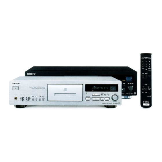
PHOTO : CDP-XB930 (BLACK Model)
SPECIFICATIONS
Semiconductor laser (λ = 780 nm)
Emission duration: continuous
Max 44.6 µW*
* This output is the value measured at
a distance of 200 mm from the
objective lens surface on the Optical
Pick-up block with 7 mm aperture.
2 Hz to 20 kHz ± 0.5 dB
More than 113 dB
More than 99 dB
Less than 0.0025%
More than 105 dB
Jack
Maximum
Load
type
output
impedance
level
Phono
2 V
Over 50 kΩ
jacks
(at 50 kΩ)
Optical
output
–18 dBm
Wave length:660nm
connector
Coaxial
0.5 Vp-p
75 Ω
output
(at 75 Ω)
connector
Stereo
32 Ω
phone
10 mW
jack
Model Name Using Similar Mechanism
CD Mechanism Type
Base Unit Type
Optical Pick-up Type
General
Power requirements
Power consumption
Dimensions (approx.)
(w/h/d)
Mass (approx.)
Supplied accessories
Audio cord (2 phono plugs–2 phono plugs) (1)
Remote commander (remote) (1)
R6 (size AA) batteries (2)
Stabilizer (1)
Design and specifications are subject to change without notice.
COMPACT DISC PLAYER
AEP Model
CDP-XB930
UK Model
E Model
CDP-XB930E
CDP-XB920/XB920E
CDM36C-14D
BU-14D
KSS-213B/K-N
220 V – 230 V AC, 50/60 Hz
15W
430 × 115 × 290 mm
(17 × 4
× 11
5
1
/
/
in.) incl.
8
2
projecting parts
6.0 kg (13 lbs 04 oz)
Advertisement
Table of Contents

Related Manuals for Sony CDP-XB930L


Summary of Contents for Sony CDP-XB930L
- Page 1 CDP-XB930/XB930E SERVICE MANUAL AEP Model CDP-XB930 UK Model E Model CDP-XB930E PHOTO : CDP-XB930 (BLACK Model) Manufactured under license from Dolby Laboratories Model Name Using Similar Mechanism CDP-XB920/XB920E Licensing Corporation. CD Mechanism Type CDM36C-14D “DOLBY” and the double-D symbol a are trademarks of Dolby Laboratories Licensing Corporation.
-
Page 2: Table Of Contents
TED LINE WITH MARK ! ON THE SCHEMATIC DIAGRAMS AND IN THE PARTS LIST ARE CRITICAL TO SAFE OPERATION. REPLACE THESE COMPO- NENTS WITH SONY PARTS WHOSE PART NUM- BERS APPEAR AS SHOWN IN THIS MANUAL OR IN SUPPLEMENTS PUBLISHED BY SONY. - Page 3 CD-TEXT TEST DISC This unit is able to display the test data (character information) written in the CD on its fluorescent indicator tube. The CD-TEXT TEST DISC (TGCS-313:4-989-366-01) is used for checking the display. To check, perform the following procedure. Checking Method: Turn ON the power, set the disc on a tray, and chuck the disc.
- Page 4 Table 2: CD-TEXT TEST DISC Recorded Contents and Display (TRACKS NO. 33 to 99) (In this unit, some special characters cannot be displayed. This is no a fault.) TRACK Recorded contents Display 100Hz/0dB/R* 1 0 0 H Z / 0 D – – – – B/R are not displayed 1kHz/0dB/R* 1 K H Z / 0 D B –...
-
Page 5: Servicing Note
SECTION 1 SERVICING NOTE HOW TO OPEN THE DISC TRAY WHEN POWER SWITCH NOTES ON HANDLING THE OPTICAL PICK-UP BLOCK TURNS OFF OR BASE UNIT The laser diode in the optical pick-up block may suffer electrostatic breakdown because of the potential difference generated by the Insert a screwdriver into the aperture of the unit bottom, and charged electrostatic load, etc. -
Page 6: General
SECTION 2 GENERAL LOCATION AND FUNCTION OF CONTROLS [FRONT PANEL] 2345 6 7 8 9!º @¡ @º !ª !• !¶ !§ @™ !£ !™ !¡ !∞ !¢ 1 U (POWER) switch !™ p (stop) button 2 PLAY MODE button !£ P (pause) button 3 REPEAT button !¢... - Page 7 This section is extracted from instruction manual.
-
Page 8: Disassembly
SECTION 3 DISASSEMBLY Note : Follow the disassembly procedure in the numerical order given. 3-1. SLIDE RACK 2 Slide rack (Disengage claws to remove the rack.) claws claws 1 Eject CD by moving "A" in the direction of the arrow. 3-2. -
Page 9: Test Mode
SECTION 4 TEST MODE 4-1. AF MODE Button No. Button No. Button Button The following checks can be performed in the AF mode, which is Displayed Displayed set by connecting the TP51 (AFADJ) terminal on MAIN board to LANGUAGE EDIT/ the Ground and turning on the power. - Page 10 4-2. ADJ MODE [MAIN BOARD] — (Component Side) — The following operations are performed in the ADJ mode, which is TP21 TP51 set by connecting the TP21 (ADJ) terminal to the Ground and turning (ADJ) (AF ADJ) on the power. R350 •...
-
Page 11: Electrical Block Checking
SECTION 5 ELECTRICAL BLOCK CHECKING Note: Note: A clear RF signal waveform means that the shape “◊” can be CD Block is basically designed to operate without adjustment. clearly distinguished at the center of the waveform. Therefore, check each item in order given. Use YEDS-18 disc (3-702-101-01) unless otherwise indicated. - Page 12 Check the level B of the oscilloscope's waveform and the A RF PLL Free-run Frequency Check (DC voltage) of the center of the Traverse waveform. Procedure : Confirm the following : Connect frequency counter to test point TP (MNT1) with lead A/B x 100 = less than ±...
-
Page 13: Diagrams
CDP-XB930/XB930E SECTION 6 DIAGRAMS 6-1. CIRCUIT BOARDS LOCATION THIS NOTE IS COMMON FOR PRINTED WIRING • Waveform BOARDS AND SCHEMATIC DIAGRAMS. TP1 (RF) (In addition to this necessary note is printed in each block.) For schematic diagrams. 1.2Vp-p KEY board Note: SERVO board •... -
Page 14: Block Diagram
CDP-XB930/XB930E 6-2. BLOCK DIAGRAM DIGITAL SERVO/ OPTICAL PICK-UP IC208 IC101 BLOCK IC251 OPTICAL • SIGNAL PATH (KSS-213B) RF AC D OUT DIGITAL DSP/ PHOTO DETECTOR RF AMP D/A CONV. IC103 IC301 IC251 J351 :DIGITAL OUT RF DC PCMD DATA CURRENT PULSE COXIAL D/A CONV. -
Page 15: Schematic Diagram Main Section (1/2)
CDP-XB930/XB930E 6-3. SCHEMATIC DIAGRAM MAIN SECTION (1/2) • Refer to page 13 for Waveforms. • Refer to page 25 for IC Block Diagram. The components identified by mark ! or dotted line with mark ! are critical for safety. Replace only with part number specified. -
Page 16: Schematic Diagram Main Section (2/2)
CDP-XB930/XB930E 6-4. SCHEMATIC DIAGRAM MAIN SECTION (2/2) • Refer to page 25 for IC Block Diagram. -
Page 17: This Caution 6-5. Printed Wiring Board Main Section
CDP-XB930/XB930E 6-5. PRINTED WIRING BOARDS MAIN SECTION • Refer to page 13 for Circuit Boards Location. • Semiconductor Location Ref. No. Location D261 D262 D263 D264 D301 D302 D303 D305 D306 D-10 D307 D-11 D308 D-11 D310 E-11 D311 D312 D351 F-11 D352... -
Page 18: Label Is Located 6-6. Schematic Diagram Display Section
CDP-XB930/XB930E 6-6. SCHEMATIC DIAGRAM DISPLAY SECTION • Refer to page 13 for Waveforms. • Refer to page 27 for IC Pin Function Description. The components identified by mark ! or dotted line with mark ! are critical for safety. Replace only with part number specified. -
Page 19: Printed Wiring Board Display Section
CDP-XB930/XB930E 6-7. PRINTED WIRING BOARDS DISPLAY SECTION • Refer to page 13 for Circuit Boards Location. • Semiconductor Location Ref. No. Location DISP BOARD D621 D958 FL501 (FLUORESCENT INDICATOR TUBE) IC801 IC802 Q621 Q801 Q802 30 31 EDIT/ TIME FADE CLEAR CHECK (12) -
Page 20: Schematic Diagram Power Section
CDP-XB930/XB930E 6-8. SCHEMATIC DIAGRAM POWER SECTION The components identified by mark ! or dotted line with mark ! are critical for safety. Replace only with part number specified. -
Page 21: Printed Wiring Board Power Section
CDP-XB930/XB930E 6-9. PRINTED WIRING BOARDS POWER SECTION • Refer to page 13 for Circuit Boards Location. • Semiconductor Location POWER BOARD TRANS BOARD Ref. No. Location D901 D902 D903 D904 D911 D912 D913 D914 D921 D922 D923 D924 SERVO D925 BOARD D951 (Page 23) -
Page 22: Schematic Diagram Servo Section
CDP-XB930/XB930E 6-10. SCHEMATIC DIAGRAM SERVO SECTION • Refer to page 13 for Waveforms. • Refer to page 26 for IC Block Diagram • Refer to page 27 for IC Pin Function Description. -
Page 23: Printed Wiring Board Servo Section
CDP-XB930/XB930E 6-11. PRINTED WIRING BOARDS SERVO SECTION • Refer to page 13 for Circuit Boards Location. • Semiconductor Location Ref. No. Location D101 D361 IC101 IC102 IC103 IC104 IC361 Q101 Q102 Q301 Q302... -
Page 24: Schematic Diagram Motor Section
CDP-XB930/XB930E 6-12. SCHEMATIC DIAGRAM MOTOR SECTION 6-13. PRINTED WIRING BOARDS MOTOR SECTION • Refer to page 13 for Circuit Boards Location. SLED BOARD SPINDLE BOARD LIMIT SW M151 SPINDLE MOTOR (11) 1-658-708- SERVO BOARD (Page 23) 1-658-709- (11) OPTICAL PICK-UP BLOCK M102 SLED MOTOR... -
Page 25: Ic Block Diagrams
6-14. IC BLOCK DIAGRAMS C301 CXD8735N (MAIN BOARD) INVO INVI BCKI TEST OVERFLOW DETECTER DATA1 128FsO FIR1 FIR2 FIR3 LRCKI DINIT FIR4 INIT OVFLAG MUTEL OVERFLOW DETECTER SHIFT MUTER FIR1 FIR2 FIR3 LATCH FIR4 SYSM 64FSI MCKIN 3rd order X0.75 NOISE L.I.P DVSS1... - Page 26 IC104 LA6510L (SERVO BOARD) VOUT2 VOUT1 VSENCE2 VSENCE1 IC103 CXA2568M (SERVO BOARD) IC302 CXA8055M (MAIN BOARD) APC PD AMP ANALOG CIREF RIREF LC/PD LD_ON VOLUME REFERENCE VREF CONTROL VOLTAGE HOLD AGND VCNT CIRCUIT CIRCUIT AGND AGCVTH VREF APC LD AMP IOR–...
-
Page 27: Ic Pin Function Description
6-15. IC PIN FUNCTION DESCRIPTION • IC 101 DIGITAL SIGNAL PROCESSOR (CXD2585Q) (SERVO board) Pin No. Pin Name Description DVDD — Digital power supply XRST System reset “L” : reset MUTE Muting input “H” : mute DATA Serial data input, supplied from CPU XLAT Latch input, supplied from CPU CLOK... - Page 28 Pin No. Pin Name Description Tracking error signal input Center servo analog input RFDC RF signal input ADIO Test pin (Not used) AVSS0 — Analog GND IGEN Stabilized current input for operation amplifiers AVDD0 — Analog power supply ASYO EFM full swing output ASYI Asymmetry comparate voltage input RFAC...
- Page 29 • IC 801 (SYSTEM CONTROL) CXP82832-017Q (DISP board) Pin No. Pin Name Description Fluorescent display tube grid 13 output Fluorescent display tube grid 14 output NC (+5V) — Not used. Connected to 5V +5 V (PEO/EC1/1NT0) — Not used. Connected to 5V SCOR Signal processing IC data sync input GND (PE2/1NT2)
- Page 30 Pin No. Pin Name Description — Not used. Open — Not used. Open — Not used. Open — Not used. Open — Not used. Open — Not used. Open — Not used. Open — Not used. Open — Not used. Open —...
-
Page 31: Exploded Views
SECTION 7 EXPLODED VIEWS NOTE: • -XX, -X mean standardized parts, so they may • The mechanical parts with no reference number The components identified by mark ! or have some differences from the original one. in the exploded views are not supplied. dotted line with mark ! are critical for safety. - Page 32 4-997-211-01 BUTTON (MODE) (BLACK) 4-950-189-01 KNOB(A) (VOL) (BLACK) 4-997-211-23 BUTTON (MODE) (SILVER) 4-950-189-61 KNOB(A) (VOL) (SILVER) 4-997-200-03 BASE(L), PANEL (BLACK) 4-942-568-41 EMBLEM (NO.5), SONY (BLACK) 4-997-200-24 BASE(L), PANEL (SILVER) 4-942-568-61 EMBLEM (NO.5), SONY (SILVER) * 64 A-4724-932-A DISP BOARD, COMPLETE...
- Page 33 7-3. MAIN SECTION not supplied T901 not supplied not supplied not supplied not supplied not supplied not supplied not supplied Ref. No. Part No. Description Remarks Ref. No. Part No. Description Remarks 3-703-249-01 SCREW, S TIGHT, +PTTWH 3 × 6 (XB930E:SP) X-4949-523-1 FOOT ASSY (F50180S) 3-703-249-21 SCREW, S TIGHT, +PTTWH (M3 ×...
- Page 34 7-4. CD MECHANISM SECTION (CDM36D-14D) Base unit not supplied M101 not supplied not supplied not supplied not supplied Ref. No. Part No. Description Remarks Ref. No. Part No. Description Remarks * 201 4-977-902-01 PANEL (DRAWER) 4-977-898-01 LEVER (SWING) 4-933-134-01 SCREW (+PTPWH M2.6 × 6) * 214 4-977-892-01 BEARING 4-986-919-01 LIMITTER (LEVER)
- Page 35 7-5. BASE UNIT SECTION (BU-14D) not supplied M151 not supplied not supplied not supplied not supplied not supplied M102 Ref. No. Part No. Description Remarks Ref. No. Part No. Description Remarks 4-977-925-01 SPRING(SLIDE BASE),COMPRESSION * 262 4-993-919-01 SPRING (A) (OP), LEAF 4-977-926-01 RACK, SLIDE 4-917-562-01 INSULATOR 4-977-923-01 SHAFT, SLED...
-
Page 36: Electrical Parts List
SECTION 8 DISP ELECTRICAL PARTS LIST NOTE: • Due to standardization, replacements in the • CAPACITORS: • SEMICONDUCTORS parts list may be different from the parts uF: µF In each case, u: µ, for example: specified in the diagrams or the components •... - Page 37 LD IN SW LOADING MAIN Ref. No. Part No. Description Remarks Ref. No. Part No. Description Remarks 1-669-372-11 HP BOARD (XB930) 1-658-710-11 LOADING BOARD ********* ************** 4-962-201-01 PLATE (HP), GROUND (XB930) < MOTOR > < CAPACITOR > M101 A-4660-968-A MOTOR ASSY (WITH PULLEY)(LOADING) ************************************************************ C350 1-162-294-31 CERAMIC...
- Page 38 MAIN Ref. No. Part No. Description Remarks Ref. No. Part No. Description Remarks C413 1-136-813-11 FILM 680PF 100V C953 1-128-197-11 ELECT 10uF C414 1-137-506-11 FILM 0.47uF C961 1-126-023-11 ELECT 100uF C415 1-125-781-21 ELECT 220uF (XB930) C419 1-101-005-00 CERAMIC 22000PF C962 1-126-023-11 ELECT 100uF C420...
- Page 39 MAIN Ref. No. Part No. Description Remarks Ref. No. Part No. Description Remarks < COIL > R342 1-259-452-11 CARBON 1/6W R350 1-259-452-11 CARBON 1/6W L251 1-410-322-11 INDUCTOR 3.3uH R351 1-259-428-11 CARBON 1/6W L252 1-410-322-11 INDUCTOR 3.3uH R352 1-259-428-11 CARBON 1/6W L302 1-410-322-11 INDUCTOR 3.3uH R353...
- Page 40 MAIN POWER POWER SW Ref. No. Part No. Description Remarks Ref. No. Part No. Description Remarks R530 1-247-690-11 CARBON 1/4W F < CONNECTOR > R531 1-247-690-11 CARBON 1/4W F R532 1-249-915-11 CARBON 1/4W CN901 1-691-771-11 PLUG (MICRO CONNECTOR) 9P R533 1-249-915-11 CARBON 1/4W CN902...
- Page 41 ROTARY SW SERVO Ref. No. Part No. Description Remarks Ref. No. Part No. Description Remarks 1-670-212-11 ROTARY SW BOARD C159 1-163-019-00 CERAMIC CHIP 0.0068uF 10% C160 1-164-690-91 CERAMIC CHIP 0.0022uF 5% **************** C161 1-164-505-11 CERAMIC CHIP 2.2uF < RESISTOR > C162 1-164-004-11 CERAMIC CHIP 0.1uF...
- Page 42 SERVO SLED SPINDLE Ref. No. Part No. Description Remarks Ref. No. Part No. Description Remarks R060 1-216-298-00 METAL CHIP 1/10W R163 1-216-105-91 RES,CHIP 220K 1/10W R061 1-216-298-00 METAL CHIP 1/10W R168 1-216-295-91 SHORT R062 1-216-298-00 METAL CHIP 1/10W R170 1-216-025-91 RES,CHIP 1/10W R063 1-216-298-00 METAL CHIP...
- Page 43 TRANS Ref. No. Part No. Description Remarks Ref. No. Part No. Description Remarks 1-669-373-12 TRANS BOARD ACCESSORIES & PACKING MATERIALS ************ ******************************** 1-473-720-11 REMOTE COMMANDER (RM-DX50) < CAPACITOR > 1-590-925-31 CORD, CONNECTION 3-866-364-11 MANUAL, INSTRUCTION ! C992 1-113-916-11 CERAMIC 0.01uF 250V (ENGLISH,FRENCH,SPANISH) ! C993...
- Page 44 CDP-XB930/XB930E Sony Corporation 9-928-931-11 99F1653-1 Home Audio Company Printed in Japan ©1999.6 Published by Quality Assurance Dept.