Sign In
Upload
Manuals
Brands
Texas Instruments Manuals
Motherboard
AM243x
Texas Instruments AM243x Manuals
Manuals and User Guides for Texas Instruments AM243x. We have
2
Texas Instruments AM243x manuals available for free PDF download: User Manual
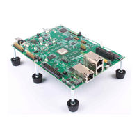
Texas Instruments AM243x User Manual (61 pages)
Brand:
Texas Instruments
| Category:
Motherboard
| Size: 3.28 MB
Table of Contents
Table of Contents
1
Introduction
3
EVM Revisions and Assembly Variants
4
Inside the Box
4
Important Usage Notes
4
Power-On Usage Note
4
EMC, EMI, and ESD Compliance
4
Table 1-1. Am64X/Am243X EVM PCB Design Revisions, and Asssembly Variants
4
System Description
5
Figure 3-1. Top View of the Am64X/Am243X EVM Board
5
Key Features
6
Figure 3-2. Bottom View of the Am64X/Am243X EVM Board
6
Functional Block Diagram
8
Figure 3-3. General Processor Board Functional Block Diagram
8
Power-On/Off Procedures
9
Power-On Procedure
9
Power-Off Procedure
10
Peripheral and Major Component Description
11
Clocking
11
Ethernet PHY Clock
11
Am64X/Am243X Clock
11
Pcie Clock
11
Figure 3-4. Am64X/Am243X EVM Clock Tree
11
Table 3-1. Source Clock Selection for the Clock Buffer
11
Reset
12
Figure 3-5. Overall Reset Architecture of the Am64X/Am243X EVM
12
Power
13
Power Input
13
Reverse Polarity Protection
13
Current Monitoring
13
Leds
13
Table 3-2. VMAIN LED
13
Table 3-3. INA Devices I2C Slave Address
13
Power Supply
14
Table 3-4. Power Test Points
14
Table 3-5. Power Leds
15
Power Sequencing
16
Figure 3-7. Power on and off Sequencing
16
Am64X/Am243X Power
17
Figure 3-8. Am64X/Am243X Core Supply and Array Core Supply Options
17
Configuration
18
Boot Modes
18
Table 3-6. Soc Power Supply
18
Figure 3-9. Am64X/Am243X EVM Schematic Excerpt, Boot Mode Selection Switches (SW2, SW3)
19
Figure 3-10. Am64X/Am243Xevm PCB, Boot Mode Selection Switches (SW2, SW3)
19
Table 3-7. BOOTMODE Bits
20
Table 3-8. PLL Reference Clock Selection BOOTMODE[2:0]
20
Table 3-9. Boot Device Selection BOOTMODE[6:3]
20
Table 3-10. Primary Boot Media Configuration BOOTMODE[9:7]
21
Table 3-11. Backup Boot Mode Selection BOOTMODE[12:10]
21
Table 3-12. Backup Boot Media Configuration BOOTMODE[13]
21
Jtag
22
Table 3-13. Selection of HSE Connector and JTAG TRACE Functionality
22
Table 3-14. TI20 Pin Connector (J25) Pin-Out
22
Figure 3-11. JTAG Interface
23
Table 3-15. TI 60-Pin Connector (J33) Pin-Out
24
Test Automation
25
Table 3-16. List of Signals Routed to Test Automation Header
25
Figure 3-12. Test Automation Header
26
Table 3-17. Test Automation Header (J38) Pin-Out
27
UART Interfaces
28
Figure 3-13. Am64X/Am243Xuart Interfaces
28
Memory Interfaces
29
DDR4 Interface
29
Figure 3-14. Am64X/Am243X DDR4 Interface
29
MMC Interfaces
30
Figure 3-15. Micro SD Interface
30
OSPI Interface
31
Figure 3-16. Emmc Interface
31
SPI EEPROM Interface
32
Board ID EEPROM Interface
32
Figure 3-17. Am64X/Am243X OSPI Interface
32
Table 3-18. Board ID Memory Header Information
32
Ethernet Interface
33
Figure 3-18. Ethernet Interface - CPSW Domain
33
Figure 3-19. Ethernet Interface - ICSSG Domain
34
DP83867 PHY Default Configuration
35
DP83869 PHY Default Configuration
35
Table 3-19. Default Strap Setting of CPSW Ethernet PHY
36
Table 3-20. Default Strap Setting of ICSSG Ethernet Phys
36
Figure 3-20. Am64X/Am243Xethernet Interfaces - CPSW Ethernet Strap Settings
38
Figure 3-21. Am64X/Am243X Ethernet Interfaces - ICSSG1 Ethernet Strap Settings
39
Figure 3-22. Am64X/Am243X Ethernet Interfaces - ICSSG2 Ethernet Strap Settings
40
Ethernet LED
41
Figure 3-23. Am64X/Am243X EVM Ethernet Interface LED
41
Display Interface
42
Table 3-21. Display Connector (J36) Pin-Out
42
USB 2.0 Interface
43
Pcie Interface
43
Figure 3-24. Am64X/Am243X USB 2.0 Host Interface
43
Figure 3-25. Am64X/Am243X Pcie Interface
44
Table 3-22. Pcie Jumper Options to Enable Root Complex and Endpoint Mode
44
Table 3-23. Pcie Connector (J27) Pin-Out
44
High Speed Expansion Interface
45
Table 3-24. Selection of PRG0 Signals on Application Connector
46
Figure 3-26. Am64X/Am243X High Speed Expansion Connector
51
CAN Interface
53
Figure 3-27. Am64X/Am243X High Speed Expansion Connector - Part
53
Figure 3-28. Am64X/Am243X High Speed Expansion Connector - Part 2
53
Table 3-25. CAN (J31 and J32) Pin-Out
53
Interrupt
54
ADC Interface
54
Figure 3-29. Am64X/Am243X CAN Interfaces
54
Table 3-26. ADC Connector (J3) Pin-Out
54
Safety Connector
55
SPI Interfaces
55
I2C Interfaces
55
Table 3-27. Safety Connector Pinouts
55
Table 3-28. I2C Test Header (J5) Pin-Out
55
Figure 3-30. Am64X/Am243X I2C Interfaces and Address Assignment of Peripherals
56
Table 3-29. I2C Test Header (J4) Pin-Out
56
FSI Interface
57
Figure 3-31. Am64X/Am243X FSI Interface
57
Table 3-30. FSI (J5) Connector Pin-Out
57
Figure 4-1. Am64X/Am243X EVM Modification Label Location
58
Table 4-1. Am64X/Am243X EVM Known Issues and Modifications
58
Figure 4-2. XDS110 CCS Connection Error Dialog
59
Figure 4-3. XDS110 Debug Reset Utility Command-Line Function
59
Advertisement
Texas Instruments AM243x User Manual (52 pages)
Brand:
Texas Instruments
| Category:
Microcontrollers
| Size: 3.36 MB
Table of Contents
Table of Contents
1
Preface: Read this First
3
If You Need Assistance
3
Important Usage Notes
3
Kit Overview
4
Figure 2-1. Am243X Launchpad Board
4
Kit Contents
5
Key Features
5
Figure 2-2. System Architecture
5
Component Identification
6
Figure 2-3. Am243X Launchpad Top Component Identification
6
Figure 2-4. Am243X Launchpad Bottom Component
6
Boosterpacks
7
Compliance
7
Security
7
Figure 2-5. Security Field Parameter
7
Board Setup
8
Power Requirements
8
Figure 3-1. USB Type-C Power Delivery Classification
8
Power Input Using USB Type-C Connector
9
Figure 3-2. Type-C CC Configuration
9
Power Status Led's
10
Figure 3-3. USB Type-C Power Input
10
Figure 3-4. Power Status Led's
10
Table 3-1. Current Sourcing Capability and State of USB Type-C Cable
10
Table 3-2. Power Status Led's
10
Power Tree
12
Figure 3-5. Power Tree Diagram of Am243X Launchpad
12
Power Sequence
13
Push Buttons
13
Figure 3-6. Power Sequence
13
Table 3-3. Launchpad Push Buttons
13
Boot Mode Selection
14
Figure 3-7. Boot-Mode DIP Switch
14
Table 3-4. Boot-Mode Selection Table
14
Hardware Description
15
Functional Block Diagram
15
Figure 4-1. Am243X Launchpad Functional Block Diagram
15
Boosterpack Headers
16
Figure 4-2. Boosterpack Header Pinout
16
Figure 4-3. Site #2 Boosterpack Header
17
Table 4-1. Boosterpack Power Sourcing for Boosterpack Site #2
17
Pinmux for Boosterpack
18
Figure 4-4. 80 Pin Boosterpack Pinout
18
Table 4-2. Pinmux Legend
19
Table 4-3. Pinmux Options for J1 Connector - Site 1
19
Table 4-4. Pinmux Options for J2 Connector - Site 1
20
Table 4-5. Pinmux Options for J3 Connector - Site 1
20
Table 4-6. Pinmux Options for J4 Connector - Site 1
20
Table 4-7. Net Name in Schematic and Package Signal Name for J1/J3 Connector
21
Table 4-8. Net Name in Schematic and Package Signal Name for J2/J4 Connector
22
Table 4-9. Pinmux Options for J5 Connector - Site 2
23
Table 4-10. Pinmux Options for J6 Connector - Site 2
23
Table 4-11. Pinmux Options for J7 Connector - Site 2
24
Table 4-12. Pinmux Options for J8 Connector - Site 2
24
Table 4-13. Net Name in Schematic and Package Signal Name for J5/J7 Connector
25
Table 4-14. Net Name in Schematic and Package Signal Name for J6/J8 Connector
26
GPIO Mapping
27
Table 4-15. GPIO Mapping Table
27
Reset
29
Figure 4-5. Reset Architecture
29
Clock
30
Figure 4-6. Clock Architecture
30
Table 4-16. Clock Frequency Table
30
Memory Interface
31
QSPI Interface
31
Figure 4-7. QSPI Interface
31
Board ID EEPROM
32
Figure 4-8. Board ID EEPROM
32
Table 4-17. Board ID Memory Header Information
32
Ethernet Interface
33
Figure 4-9. Ethernet Connection
33
Ethernet PHY Strapping
34
Figure 4-10. CPSW or PRG RGMII1 Ethernet Data Mux
34
Figure 4-11. Ethernet PHY Strapping for RGMII1 PHY
35
Figure 4-12. Ethernet PHY Strapping for RGMII2 PHY
35
Ethernet PHY - Power, Clock, Reset, Interrupt
36
LED Indication in Ethernet RJ45 Connector
36
Table 4-18. Ethernet PHY Strapping Values
36
USB 2.0 Interface
37
I2C Interface
37
Figure 4-13. USB 2.0 Interface
37
Figure 4-14. I2C Interface
37
Industrial Application Leds
38
Figure 4-15. Industrial Application Leds
38
UART Interface
39
Figure 4-16. UART Interface
39
Eqep Interface
40
Figure 4-17. Eqep Interface
40
Figure 4-18. Eqep1 Header
40
Figure 4-19. Eqep2 Header
41
Figure 4-20. Eqep2 or MCAN0 Mux Selection Circuit
41
CAN Interface
42
Figure 4-21. CAN Interface
42
Figure 4-22. MCAN Transceiver and Header
42
FSI Interface
43
Figure 4-23. FSI Interface
43
Table 4-19. FSI Header Pin Description
43
Figure 4-24. FSI Header
44
Figure 4-25. FSI or Boosterpack Mux Selection Circuit
44
JTAG Emulation
45
Figure 4-26. JTAG Interface
45
Figure 4-27. Micro-B USB Connection for JTAG
45
Test Automation Interface
46
Figure 4-28. Test Automation Header
46
Table 4-20. Test Automation Signal Description
46
Table 4-21. Test Automation Header Pinout
47
SPI Interface
48
Figure 4-29. SPI Connection from Soc to Boosterpack Connector
48
Reference Documents
49
Other TI Components Used in this Design
49
Revision History
49
A E3 Design Changes
50
Table A-1. E3 RJ45 Connector
50
Table A-2. E3 GPIO Mapping
50
Table A-3. E3 Ethernet PHY Signal Mapping
51
Table A-4. E3 LED ACT Signal Resistor Mounting
51
Advertisement
Related Products
Texas Instruments AM263 Series
Texas Instruments AM2631
Texas Instruments AM2632
Texas Instruments AM2634
Texas Instruments AM2632-Q1
Texas Instruments AM2631-Q1
Texas Instruments AM2634-Q1
Texas Instruments AM273x
Texas Instruments BoosterPack AM2 BLDC Series
Texas Instruments AM263P-SIP Series
Texas Instruments Categories
Motherboard
Control Unit
Microcontrollers
Computer Hardware
Calculator
More Texas Instruments Manuals
Login
Sign In
OR
Sign in with Facebook
Sign in with Google
Upload manual
Upload from disk
Upload from URL