Sign In
Upload
Manuals
Brands
ST Manuals
Controller
STM32F105 series
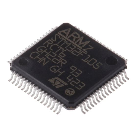
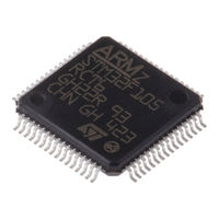
ST STM32F105 series Manuals
Manuals and User Guides for ST STM32F105 series. We have
3
ST STM32F105 series manuals available for free PDF download: Reference Manual, Application Note
ST STM32F105 series Reference Manual (1128 pages)
advanced ARM-based 32-bit MCUs
Brand:
ST
| Category:
Controller
| Size: 11 MB
Table of Contents
Table of Contents
2
Overview of the Manual
40
Table 1. Sections Related to each Stm32F10Xxx Product
40
Table 2. Sections Related to each Peripheral
43
Documentation Conventions
47
List of Abbreviations for Registers
47
Glossary
47
Peripheral Availability
47
Memory and Bus Architecture
48
System Architecture
48
Figure 1. System Architecture (Low-, Medium-, XL-Density Devices)
48
Figure 2. System Architecture in Connectivity Line Devices
49
Memory Organization
50
Memory Map
51
Table 3. Register Boundary Addresses
51
Bit Banding
54
Embedded SRAM
54
Embedded Flash Memory
55
Table 4. Flash Module Organization (Low-Density Devices)
55
Table 5. Flash Module Organization (Medium-Density Devices)
56
Table 6. Flash Module Organization (High-Density Devices)
57
Table 7. Flash Module Organization (Connectivity Line Devices)
57
Table 8. XL-Density Flash Module Organization
58
Boot Configuration
61
Table 9. Boot Modes
61
CRC Calculation Unit
64
CRC Introduction
64
CRC Main Features
64
Figure 3. CRC Calculation Unit Block Diagram
64
CRC Functional Description
65
CRC Registers
65
Data Register (CRC_DR)
65
Independent Data Register (CRC_IDR)
65
Control Register (CRC_CR)
66
CRC Register Map
66
Table 10. CRC Calculation Unit Register Map and Reset Values
66
Power Control (PWR)
67
Power Supplies
67
Independent A/D and D/A Converter Supply and Reference Voltage
68
Figure 4. Power Supply Overview
68
Battery Backup Domain
69
Voltage Regulator
70
Power Supply Supervisor
70
Power on Reset (Por)/Power down Reset (PDR)
70
Programmable Voltage Detector (PVD)
70
Figure 5. Power on Reset/Power down Reset Waveform
70
Figure 6. PVD Thresholds
71
Low-Power Modes
72
Slowing down System Clocks
72
Table 11. Low-Power Mode Summary
72
Peripheral Clock Gating
73
Sleep Mode
73
Stop Mode
74
Table 12. Sleep-Now
74
Table 13. Sleep-On-Exit
74
Table 14. Stop Mode
75
Standby Mode
76
Table 15. Standby Mode
76
Auto-Wakeup (AWU) from Low-Power Mode
77
Power Control Registers
77
Power Control Register (PWR_CR)
77
Power Control/Status Register (PWR_CSR)
79
PWR Register Map
80
Table 16. PWR Register Map and Reset Values
80
Backup Registers (BKP)
81
BKP Introduction
81
BKP Main Features
81
BKP Functional Description
82
Tamper Detection
82
RTC Calibration
82
BKP Registers
83
Backup Data Register X (Bkp_Drx) (X = 1
83
RTC Clock Calibration Register (BKP_RTCCR)
83
Backup Control Register (BKP_CR)
84
Backup Control/Status Register (BKP_CSR)
84
BKP Register Map
85
Table 17. BKP Register Map and Reset Values
85
Low-, Medium-, High- and XL-Density Reset and Clock Control (RCC)
90
Reset
90
System Reset
90
Power Reset
91
Figure 7. Simplified Diagram of the Reset Circuit
91
Backup Domain Reset
92
Clocks
92
Figure 8. Clock Tree
93
Figure 9. HSE/ LSE Clock Sources
94
HSE Clock
94
HSI Clock
95
Pll
96
LSE Clock
96
LSI Clock
96
System Clock (SYSCLK) Selection
97
Clock Security System (CSS)
97
RTC Clock
98
Watchdog Clock
98
Clock-Out Capability
98
RCC Registers
99
Clock Control Register (RCC_CR)
99
Clock Configuration Register (RCC_CFGR)
101
Clock Interrupt Register (RCC_CIR)
104
APB2 Peripheral Reset Register (RCC_APB2RSTR)
106
APB1 Peripheral Reset Register (RCC_APB1RSTR)
109
AHB Peripheral Clock Enable Register (RCC_AHBENR)
111
APB2 Peripheral Clock Enable Register (RCC_APB2ENR)
112
APB1 Peripheral Clock Enable Register (RCC_APB1ENR)
115
Backup Domain Control Register (RCC_BDCR)
118
Control/Status Register (RCC_CSR)
119
RCC Register Map
121
Table 18. RCC Register Map and Reset Values
121
Connectivity Line Devices: Reset and Clock Control (RCC)
123
Reset
123
System Reset
123
Power Reset
124
Figure 10. Simplified Diagram of the Reset Circuit
124
Backup Domain Reset
125
Clocks
125
Figure 11. Clock Tree
126
HSE Clock
127
Figure 12. HSE/ LSE Clock Sources
128
HSI Clock
128
LSE Clock
129
Plls
129
LSI Clock
130
System Clock (SYSCLK) Selection
130
Clock Security System (CSS)
131
RTC Clock
131
Watchdog Clock
131
Clock-Out Capability
132
RCC Registers
132
Clock Control Register (RCC_CR)
132
Clock Configuration Register (RCC_CFGR)
134
Clock Interrupt Register (RCC_CIR)
137
APB2 Peripheral Reset Register (RCC_APB2RSTR)
141
APB1 Peripheral Reset Register (RCC_APB1RSTR)
142
AHB Peripheral Clock Enable Register (RCC_AHBENR)
145
APB2 Peripheral Clock Enable Register (RCC_APB2ENR)
146
APB1 Peripheral Clock Enable Register (RCC_APB1ENR)
148
Backup Domain Control Register (RCC_BDCR)
150
Control/Status Register (RCC_CSR)
152
AHB Peripheral Clock Reset Register (RCC_AHBRSTR)
153
Clock Configuration Register2 (RCC_CFGR2)
154
RCC Register Map
156
Table 19. RCC Register Map and Reset Values
156
General-Purpose and Alternate-Function I/Os (Gpios and Afios)
159
GPIO Functional Description
159
Figure 13. Basic Structure of a Standard I/O Port Bit
160
Figure 14. Basic Structure of a Five-Volt Tolerant I/O Port Bit
160
Atomic Bit Set or Reset
161
General-Purpose I/O (GPIO)
161
Table 20. Port Bit Configuration Table
161
Table 21. Output MODE Bits
161
Alternate Functions (AF)
162
External Interrupt/Wakeup Lines
162
GPIO Locking Mechanism
162
Software Remapping of I/O Alternate Functions
162
Figure 15. Input Floating/Pull Up/Pull down Configurations
163
Input Configuration
163
Figure 16. Output Configuration
164
Output Configuration
164
Alternate Function Configuration
165
Figure 17. Alternate Function Configuration
165
Analog Configuration
166
Figure 18. High Impedance-Analog Configuration
166
GPIO Configurations for Device Peripherals
166
Table 22. Advanced Timers TIM1/TIM8
166
Table 23. General-Purpose Timers TIM2/3/4/5
167
Table 24. Usarts
167
Table 25. SPI
167
Table 26. I2S
168
Table 27. I2C
168
Table 28. Bxcan
168
Table 29. USB
168
Table 30. OTG_FS Pin Configuration
168
Figure 19. ADC / DAC
169
Table 31. SDIO
169
Table 32. FSMC
169
Table 33. Other Ios
170
GPIO Registers
171
Port Configuration Register Low (Gpiox_Crl) (X=A..g
171
Port Configuration Register High (Gpiox_Crh) (X=A..g
172
Port Input Data Register (Gpiox_Idr) (X=A..g
172
Port Output Data Register (Gpiox_Odr) (X=A
173
Port Bit Set/Reset Register (Gpiox_Bsrr) (X=A
173
Port Bit Reset Register (Gpiox_Brr) (X=A
174
Port Configuration Lock Register (Gpiox_Lckr) (X=A
174
Alternate Function I/O and Debug Configuration (AFIO)
175
Using OSC32_IN/OSC32_OUT Pins as GPIO Ports PC14/PC15
175
Using OSC_IN/OSC_OUT Pins as GPIO Ports PD0/PD1
175
CAN1 Alternate Function Remapping
176
CAN2 Alternate Function Remapping
176
JTAG/SWD Alternate Function Remapping
176
Table 34. CAN1 Alternate Function Remapping
176
Table 35. CAN2 Alternate Function Remapping
176
Table 36. Debug Interface Signals
176
ADC Alternate Function Remapping
177
Table 37. Debug Port Mapping
177
Table 38. ADC1 External Trigger Injected Conversion Alternate Function Remapping
177
Table 39. ADC1 External Trigger Regular Conversion Alternate Function Remapping
177
Table 40. ADC2 External Trigger Injected Conversion Alternate Function Remapping
177
Timer Alternate Function Remapping
178
Table 41. ADC2 External Trigger Regular Conversion Alternate Function Remapping
178
Table 42. TIM5 Alternate Function Remapping
178
Table 43. TIM4 Alternate Function Remapping
178
Table 44. TIM3 Alternate Function Remapping
178
Table 45. TIM2 Alternate Function Remapping
179
Table 46. TIM1 Alternate Function Remapping
179
Table 47. TIM9 Remapping
179
Table 48. TIM10 Remapping
179
USART Alternate Function Remapping
180
Table 49. TIM11 Remapping
180
Table 50. TIM13 Remapping
180
Table 51. TIM14 Remapping
180
Table 52. USART3 Remapping
180
Table 53. USART2 Remapping
180
I2C1 Alternate Function Remapping
181
SPI1 Alternate Function Remapping
181
SPI3/I2S3 Alternate Function Remapping
181
Ethernet Alternate Function Remapping
181
Table 54. USART1 Remapping
181
Table 55. I2C1 Remapping
181
Table 56. SPI1 Remapping
181
Table 57. SPI3/I2S3 Remapping
181
Table 58. ETH Remapping
182
AFIO Registers
183
Event Control Register (AFIO_EVCR)
183
AF Remap and Debug I/O Configuration Register (AFIO_MAPR)
184
External Interrupt Configuration Register 1 (AFIO_EXTICR1)
191
External Interrupt Configuration Register 2 (AFIO_EXTICR2)
191
External Interrupt Configuration Register 3 (AFIO_EXTICR3)
192
External Interrupt Configuration Register 4 (AFIO_EXTICR4)
192
AF Remap and Debug I/O Configuration Register2 (AFIO_MAPR2)
193
GPIO and AFIO Register Maps
194
Table 59. GPIO Register Map and Reset Values
194
Table 60. AFIO Register Map and Reset Values
194
Interrupts and Events
196
Nested Vectored Interrupt Controller (NVIC)
196
Systick Calibration Value Register
196
Interrupt and Exception Vectors
197
Table 61. Vector Table for Connectivity Line Devices
197
Table 62. Vector Table for XL-Density Devices
200
Table 63. Vector Table for Other Stm32F10Xxx Devices
203
External Interrupt/Event Controller (EXTI)
205
Main Features
206
Block Diagram
206
Wakeup Event Management
206
Figure 20. External Interrupt/Event Controller Block Diagram
206
Functional Description
207
External Interrupt/Event Line Mapping
208
Figure 21. External Interrupt/Event GPIO Mapping
208
EXTI Registers
210
Interrupt Mask Register (EXTI_IMR)
210
Event Mask Register (EXTI_EMR)
210
Rising Trigger Selection Register (EXTI_RTSR)
211
Falling Trigger Selection Register (EXTI_FTSR)
211
Software Interrupt Event Register (EXTI_SWIER)
212
Pending Register (EXTI_PR)
212
EXTI Register Map
213
Table 64. External Interrupt/Event Controller Register Map and Reset Values
213
Analog-To-Digital Converter (ADC)
214
ADC Introduction
214
ADC Main Features
215
ADC Functional Description
215
Figure 22. Single ADC Block Diagram
216
Table 65. ADC Pins
217
ADC Clock
218
ADC On-Off Control
218
Channel Selection
218
Single Conversion Mode
218
Continuous Conversion Mode
219
Figure 23. Timing Diagram
219
Timing Diagram
219
Analog Watchdog
220
Figure 24. Analog Watchdog Guarded Area
220
Scan Mode
220
Table 66. Analog Watchdog Channel Selection
220
Figure 25. Injected Conversion Latency
221
Injected Channel Management
221
Discontinuous Mode
222
Calibration
222
Data Alignment
223
Figure 26. Calibration Timing Diagram
223
Figure 27. Right Alignment of Data
223
Figure 28. Left Alignment of Data
223
Channel-By-Channel Programmable Sample Time
224
Conversion on External Trigger
224
Table 67. External Trigger for Regular Channels for ADC1 and ADC2
224
Table 68. External Trigger for Injected Channels for ADC1 and ADC2
225
Table 69. External Trigger for Regular Channels for ADC3
225
Table 70. External Trigger for Injected Channels for ADC3
225
DMA Request
226
Dual ADC Mode
227
Figure 29. Dual ADC Block Diagram
228
Figure 30. Injected Simultaneous Mode on 4 Channels
229
Injected Simultaneous Mode
229
Regular Simultaneous Mode
229
Fast Interleaved Mode
230
Figure 31. Regular Simultaneous Mode on 16 Channels
230
Figure 32. Fast Interleaved Mode on 1 Channel in Continuous Conversion Mode
230
Slow Interleaved Mode
230
Alternate Trigger Mode
231
Figure 33. Slow Interleaved Mode on 1 Channel
231
Figure 34. Alternate Trigger: Injected Channel Group of each ADC
231
Combined Regular Simultaneous + Alternate Trigger Mode
232
Combined Regular/Injected Simultaneous Mode
232
Figure 35. Alternate Trigger: 4 Injected Channels (each ADC) in Discontinuous Model
232
Independent Mode
232
Combined Injected Simultaneous + Interleaved
233
Figure 36. Alternate + Regular Simultaneous
233
Figure 37. Case of Trigger Occurring During Injected Conversion
233
Figure 38. Interleaved Single Channel with Injected Sequence CH11, CH12
233
Temperature Sensor
234
Figure 39. Temperature Sensor and VREFINT Channel Block Diagram
234
ADC Interrupts
235
Table 71. ADC Interrupts
235
ADC Registers
236
ADC Status Register (ADC_SR)
236
ADC Control Register 1 (ADC_CR1)
237
ADC Control Register 2 (ADC_CR2)
239
ADC Sample Time Register 1 (ADC_SMPR1)
243
ADC Sample Time Register 2 (ADC_SMPR2)
244
ADC Injected Channel Data Offset Register X (Adc_Jofrx)(X=1
244
ADC Watchdog High Threshold Register (ADC_HTR)
245
ADC Watchdog Low Threshold Register (ADC_LTR)
245
ADC Regular Sequence Register 1 (ADC_SQR1)
246
ADC Regular Sequence Register 2 (ADC_SQR2)
247
ADC Regular Sequence Register 3 (ADC_SQR3)
248
ADC Injected Sequence Register (ADC_JSQR)
249
ADC Injected Data Register X (Adc_Jdrx) (X= 1
250
ADC Regular Data Register (ADC_DR)
250
11.12.15 ADC Register Map
251
Table 72. ADC Register Map and Reset Values
251
Digital-To-Analog Converter (DAC)
253
DAC Introduction
253
DAC Main Features
253
Table 73. DAC Pins
254
Figure 40. DAC Channel Block Diagram
254
DAC Functional Description
255
DAC Channel Enable
255
DAC Output Buffer Enable
255
DAC Data Format
255
DAC Conversion
256
Figure 41. Data Registers in Single DAC Channel Mode
256
Figure 42. Data Registers in Dual DAC Channel Mode
256
DAC Output Voltage
257
DAC Trigger Selection
257
Table 74. External Triggers
257
Figure 43. Timing Diagram for Conversion with Trigger Disabled TEN = 0
257
DMA Request
258
Noise Generation
258
Figure 44. DAC LFSR Register Calculation Algorithm
258
Triangle-Wave Generation
259
Figure 45. DAC Conversion (SW Trigger Enabled) with LFSR Wave Generation
259
Figure 46. DAC Triangle Wave Generation
259
Dual DAC Channel Conversion
260
Independent Trigger Without Wave Generation
260
Figure 47. DAC Conversion (SW Trigger Enabled) with Triangle Wave Generation
260
Independent Trigger with same LFSR Generation
261
Independent Trigger with Different LFSR Generation
261
Independent Trigger with same Triangle Generation
261
Independent Trigger with Different Triangle Generation
262
Simultaneous Software Start
262
Simultaneous Trigger Without Wave Generation
262
Simultaneous Trigger with same LFSR Generation
263
Simultaneous Trigger with Different LFSR Generation
263
Simultaneous Trigger with same Triangle Generation
263
Simultaneous Trigger with Different Triangle Generation
264
DAC Registers
264
DAC Control Register (DAC_CR)
264
DAC Software Trigger Register (DAC_SWTRIGR)
267
DAC Channel1 12-Bit Right-Aligned Data Holding Register
268
(Dac_Dhr12R1)
268
DAC Channel1 12-Bit Left Aligned Data Holding Register
268
(Dac_Dhr12L1)
268
DAC Channel1 8-Bit Right Aligned Data Holding Register
268
(Dac_Dhr8R1)
268
DAC Channel2 12-Bit Right Aligned Data Holding Register
269
(Dac_Dhr12R2)
269
DAC Channel2 12-Bit Left Aligned Data Holding Register
269
(Dac_Dhr12L2)
269
DAC Channel2 8-Bit Right-Aligned Data Holding Register
269
(Dac_Dhr8R2)
269
Dual DAC 12-Bit Right-Aligned Data Holding Register (DAC_DHR12RD)
270
DUAL DAC 12-Bit Left Aligned Data Holding Register
270
(Dac_Dhr12Ld)
270
DUAL DAC 8-Bit Right Aligned Data Holding Register
271
(Dac_Dhr8Rd)
271
DAC Channel1 Data Output Register (DAC_DOR1)
271
DAC Channel2 Data Output Register (DAC_DOR2)
271
DAC Register Map
272
Table 75. DAC Register Map
272
Direct Memory Access Controller (DMA)
273
DMA Introduction
273
DMA Main Features
273
Figure 48. DMA Block Diagram in Connectivity Line Devices
274
DMA Functional Description
275
DMA Transactions
275
Figure 49. DMA Block Diagram in Low-, Medium- High- and XL-Density Devices
275
Arbiter
276
DMA Channels
276
Programmable Data Width, Data Alignment and Endians
278
Table 76. Programmable Data Width & Endian Behavior (When Bits PINC = MINC = 1)
278
Error Management
279
Interrupts
280
DMA Request Mapping
280
Table 77. DMA Interrupt Requests
280
Figure 50. DMA1 Request Mapping
280
Table 78. Summary of DMA1 Requests for each Channel
282
Table 79. Summary of DMA2 Requests for each Channel
283
Figure 51. DMA2 Request Mapping
283
DMA Registers
284
DMA Interrupt Status Register (DMA_ISR)
284
DMA Interrupt Flag Clear Register (DMA
285
DMA Channel X Configuration Register (Dma_Ccrx) (X = 1
286
DMA Channel X Number of Data Register (Dma_Cndtrx) (X = 1
287
DMA Channel X Peripheral Address Register (Dma_Cparx) (X = 1
288
DMA Channel X Memory Address Register (Dma_Cmarx) (X = 1
288
DMA Register Map
289
Table 80. DMA Register Map and Reset Values
289
Advanced-Control Timers (TIM1&TIM8)
292
TIM1&TIM8 Introduction
292
TIM1&TIM8 Main Features
293
Figure 52. Advanced-Control Timer Block Diagram
294
TIM1&TIM8 Functional Description
295
Time-Base Unit
295
Counter Modes
296
Figure 53. Counter Timing Diagram with Prescaler Division Change from 1 to 2
296
Figure 54. Counter Timing Diagram with Prescaler Division Change from 1 to 4
296
Figure 55. Counter Timing Diagram, Internal Clock Divided by 1
297
Figure 56. Counter Timing Diagram, Internal Clock Divided by 2
297
Figure 57. Counter Timing Diagram, Internal Clock Divided by 4
298
Figure 58. Counter Timing Diagram, Internal Clock Divided by N
298
Figure 59. Counter Timing Diagram, Update Event When ARPE=0 (Timx_Arr Not Preloaded)
298
Figure 60. Counter Timing Diagram, Update Event When ARPE=1
299
Figure 61. Counter Timing Diagram, Internal Clock Divided by 1
300
Figure 62. Counter Timing Diagram, Internal Clock Divided by 2
300
Figure 63. Counter Timing Diagram, Internal Clock Divided by 4
300
Figure 64. Counter Timing Diagram, Internal Clock Divided by N
301
Figure 65. Counter Timing Diagram, Update Event When Repetition Counter
301
Figure 66. Counter Timing Diagram, Internal Clock Divided by 1, Timx_Arr = 0X6
302
Figure 67. Counter Timing Diagram, Internal Clock Divided by 2
303
Figure 68. Counter Timing Diagram, Internal Clock Divided by 4, Timx_Arr=0X36
303
Figure 69. Counter Timing Diagram, Internal Clock Divided by N
303
Repetition Counter
304
Figure 70. Counter Timing Diagram, Update Event with ARPE=1 (Counter Underflow)
304
Figure 71. Counter Timing Diagram, Update Event with ARPE=1 (Counter Overflow)
304
Figure 72. Update Rate Examples Depending on Mode and Timx_Rcr Register Settings
305
Clock Selection
306
Figure 73. Control Circuit in Normal Mode, Internal Clock Divided by 1
306
Figure 74. TI2 External Clock Connection Example
306
Figure 75. Control Circuit in External Clock Mode 1
307
Figure 76. External Trigger Input Block
307
Capture/Compare Channels
308
Figure 77. Control Circuit in External Clock Mode 2
308
Figure 78. Capture/Compare Channel (Example: Channel 1 Input Stage)
309
Figure 79. Capture/Compare Channel 1 Main Circuit
309
Input Capture Mode
310
Figure 80. Output Stage of Capture/Compare Channel (Channel 1 to 3)
310
Figure 81. Output Stage of Capture/Compare Channel (Channel 4)
310
PWM Input Mode
311
Forced Output Mode
312
Figure 82. PWM Input Mode Timing
312
Output Compare Mode
313
PWM Mode
314
Figure 83. Output Compare Mode, Toggle on OC1
314
Figure 84. Edge-Aligned PWM Waveforms (ARR=8)
315
Figure 85. Center-Aligned PWM Waveforms (ARR=8)
316
Complementary Outputs and Dead-Time Insertion
317
Figure 86. Complementary Output with Dead-Time Insertion
317
Figure 87. Dead-Time Waveforms with Delay Greater than the Negative Pulse
317
Using the Break Function
318
Figure 88. Dead-Time Waveforms with Delay Greater than the Positive Pulse
318
Figure 89. Output Behavior in Response to a Break
320
Clearing the Ocxref Signal on an External Event
321
Figure 90. Clearing Timx Ocxref
321
6-Step PWM Generation
322
Figure 91. 6-Step Generation, COM Example (OSSR=1)
322
One-Pulse Mode
323
Figure 92. Example of One Pulse Mode
323
Encoder Interface Mode
324
Table 81. Counting Direction Versus Encoder Signals
325
Timer Input XOR Function
326
Figure 93. Example of Counter Operation in Encoder Interface Mode
326
Figure 94. Example of Encoder Interface Mode with TI1FP1 Polarity Inverted
326
Interfacing with Hall Sensors
327
Figure 95. Example of Hall Sensor Interface
328
Timx and External Trigger Synchronization
329
Figure 96. Control Circuit in Reset Mode
329
Figure 97. Control Circuit in Gated Mode
330
Figure 98. Control Circuit in Trigger Mode
331
Timer Synchronization
332
Debug Mode
332
Figure 99. Control Circuit in External Clock Mode 2 + Trigger Mode
332
TIM1&TIM8 Registers
333
TIM1&TIM8 Control Register 1 (Timx_Cr1)
333
TIM1&TIM8 Control Register 2 (Timx_Cr2)
334
TIM1&TIM8 Slave Mode Control Register (Timx_Smcr)
337
TIM1&TIM8 Dma/Interrupt Enable Register (Timx_Dier)
339
Table 82. Timx Internal Trigger Connection
339
TIM1&TIM8 Status Register (Timx_Sr)
341
TIM1&TIM8 Event Generation Register (Timx_Egr)
342
TIM1&TIM8 Capture/Compare Mode Register 1 (Timx_Ccmr1)
344
TIM1&TIM8 Capture/Compare Mode Register 2 (Timx_Ccmr2)
347
TIM1&TIM8 Capture/Compare Enable Register (Timx_Ccer)
348
Table 83. Output Control Bits for Complementary Ocx and Ocxn Channels with
350
Break Feature
350
TIM1&TIM8 Counter (Timx_Cnt)
351
TIM1&TIM8 Prescaler (Timx_Psc)
351
TIM1&TIM8 Auto-Reload Register (Timx_Arr)
351
TIM1&TIM8 Repetition Counter Register (Timx_Rcr)
352
TIM1&TIM8 Capture/Compare Register 1 (Timx_Ccr1)
352
TIM1&TIM8 Capture/Compare Register 2 (Timx_Ccr2)
353
TIM1&TIM8 Capture/Compare Register 3 (Timx_Ccr3)
353
TIM1&TIM8 Capture/Compare Register 4 (Timx_Ccr4)
354
TIM1&TIM8 Break and Dead-Time Register (Timx_Bdtr)
354
TIM1&TIM8 DMA Control Register (Timx_Dcr)
356
TIM1&TIM8 DMA Address for Full Transfer (Timx_Dmar)
357
TIM1&TIM8 Register Map
358
Table 84. TIM1&TIM8 Register Map and Reset Values
358
General-Purpose Timers (TIM2 to TIM5)
360
TIM2 to TIM5 Introduction
360
Timx Main Features
361
Timx Functional Description
362
Time-Base Unit
362
Figure 100. General-Purpose Timer Block Diagram
362
Figure 101. Counter Timing Diagram with Prescaler Division Change from 1 to 2
363
Counter Modes
364
Figure 102. Counter Timing Diagram with Prescaler Division Change from 1 to 4
364
Figure 103. Counter Timing Diagram, Internal Clock Divided by 1
365
Figure 104. Counter Timing Diagram, Internal Clock Divided by 2
365
Figure 105. Counter Timing Diagram, Internal Clock Divided by 4
365
Figure 106. Counter Timing Diagram, Internal Clock Divided by N
366
Figure 107. Counter Timing Diagram, Update Event When ARPE=0 (Timx_Arr Not Preloaded)
366
Figure 108. Counter Timing Diagram, Update Event When ARPE=1 (Timx_Arr Preloaded)
367
Figure 109. Counter Timing Diagram, Internal Clock Divided by 1
368
Figure 110. Counter Timing Diagram, Internal Clock Divided by 2
368
Figure 111. Counter Timing Diagram, Internal Clock Divided by 4
368
Figure 112. Counter Timing Diagram, Internal Clock Divided by N
369
Figure 113. Counter Timing Diagram, Update Event
369
Figure 114. Counter Timing Diagram, Internal Clock Divided by 1, Timx_Arr=0X6
370
Figure 115. Counter Timing Diagram, Internal Clock Divided by 2
371
Figure 116. Counter Timing Diagram, Internal Clock Divided by 4, Timx_Arr=0X36
371
Figure 117. Counter Timing Diagram, Internal Clock Divided by N
371
Clock Selection
372
Figure 118. Counter Timing Diagram, Update Event with ARPE=1 (Counter Underflow)
372
Figure 119. Counter Timing Diagram, Update Event with ARPE=1 (Counter Overflow)
372
Figure 120. Control Circuit in Normal Mode, Internal Clock Divided by 1
373
Figure 121. TI2 External Clock Connection Example
373
Figure 122. Control Circuit in External Clock Mode 1
374
Figure 123. External Trigger Input Block
374
Capture/Compare Channels
375
Figure 124. Control Circuit in External Clock Mode 2
375
Figure 125. Capture/Compare Channel (Example: Channel 1 Input Stage)
375
Figure 126. Capture/Compare Channel 1 Main Circuit
376
Figure 127. Output Stage of Capture/Compare Channel (Channel 1)
376
Input Capture Mode
377
PWM Input Mode
378
Figure 128. PWM Input Mode Timing
378
Forced Output Mode
379
Output Compare Mode
379
PWM Mode
380
Figure 129. Output Compare Mode, Toggle on OC1
380
Figure 130. Edge-Aligned PWM Waveforms (ARR=8)
381
Figure 131. Center-Aligned PWM Waveforms (ARR=8)
382
One-Pulse Mode
383
Figure 132. Example of One-Pulse Mode
383
Clearing the Ocxref Signal on an External Event
384
Encoder Interface Mode
385
Figure 133. Clearing Timx Ocxref
385
Table 85. Counting Direction Versus Encoder Signals
386
Figure 134. Example of Counter Operation in Encoder Interface Mode
387
Figure 135. Example of Encoder Interface Mode with TI1FP1 Polarity Inverted
387
Timer Input XOR Function
388
Timers and External Trigger Synchronization
388
Figure 136. Control Circuit in Reset Mode
388
Figure 137. Control Circuit in Gated Mode
389
Figure 138. Control Circuit in Trigger Mode
390
Timer Synchronization
391
Figure 139. Control Circuit in External Clock Mode 2 + Trigger Mode
391
Figure 140. Master/Slave Timer Example
391
Figure 141. Gating Timer 2 with OC1REF of Timer 1
392
Figure 142. Gating Timer 2 with Enable of Timer 1
393
Figure 143. Triggering Timer 2 with Update of Timer 1
394
Figure 144. Triggering Timer 2 with Enable of Timer 1
394
Debug Mode
396
Figure 145. Triggering Timer 1 and 2 with Timer 1 TI1 Input
396
Timx2 to TIM5 Registers
397
Timx Control Register 1 (Timx_Cr1)
397
Timx Control Register 2 (Timx_Cr2)
399
Timx Slave Mode Control Register (Timx_Smcr)
400
Table 86. Timx Internal Trigger Connection
401
Timx Dma/Interrupt Enable Register (Timx_Dier)
402
Timx Status Register (Timx_Sr)
403
Timx Event Generation Register (Timx_Egr)
405
Timx Capture/Compare Mode Register 1 (Timx_Ccmr1)
406
Timx Capture/Compare Mode Register 2 (Timx_Ccmr2)
409
Timx Capture/Compare Enable Register (Timx_Ccer)
410
Timx Counter (Timx_Cnt)
411
Table 87. Output Control Bit for Standard Ocx Channels
411
Timx Prescaler (Timx_Psc)
412
Timx Auto-Reload Register (Timx_Arr)
412
Timx Capture/Compare Register 1 (Timx_Ccr1)
412
Timx Capture/Compare Register 2 (Timx_Ccr2)
413
Timx Capture/Compare Register 3 (Timx_Ccr3)
413
Timx Capture/Compare Register 4 (Timx_Ccr4)
413
Timx DMA Control Register (Timx_Dcr)
414
Timx DMA Address for Full Transfer (Timx_Dmar)
414
Timx Register Map
416
Table 88. Timx Register Map and Reset Values
416
General-Purpose Timers (TIM9 to TIM14)
418
TIM9 to TIM14 Introduction
418
TIM9 to TIM14 Main Features
419
TIM9/TIM12 Main Features
419
Figure 146. General-Purpose Timer Block Diagram (TIM9 and TIM12)
419
TIM10/TIM11 and TIM13/TIM14 Main Features
420
Figure 147. General-Purpose Timer Block Diagram (TIM10/11/13/14)
420
TIM9 to TIM14 Functional Description
421
Time-Base Unit
421
Counter Modes
422
Figure 148. Counter Timing Diagram with Prescaler Division Change from 1 to 2
422
Figure 149. Counter Timing Diagram with Prescaler Division Change from 1 to 4
422
Figure 150. Counter Timing Diagram, Internal Clock Divided by 1
423
Figure 151. Counter Timing Diagram, Internal Clock Divided by 2
423
Figure 152. Counter Timing Diagram, Internal Clock Divided by 4
424
Figure 153. Counter Timing Diagram, Internal Clock Divided by N
424
Clock Selection
425
Figure 156. Control Circuit in Normal Mode, Internal Clock Divided by 1
426
Figure 157. TI2 External Clock Connection Example
426
Capture/Compare Channels
427
Figure 158. Control Circuit in External Clock Mode 1
427
Figure 159. Capture/Compare Channel (Example: Channel 1 Input Stage)
427
Input Capture Mode
428
Figure 160. Capture/Compare Channel 1 Main Circuit
428
Figure 161. Output Stage of Capture/Compare Channel (Channel 1)
428
PWM Input Mode (Only for TIM9/12)
429
Forced Output Mode
430
Figure 162. PWM Input Mode Timing
430
Output Compare Mode
431
PWM Mode
432
Figure 163. Output Compare Mode, Toggle on OC1
432
One-Pulse Mode
433
Figure 164. Edge-Aligned PWM Waveforms (ARR=8)
433
Figure 165. Example of One Pulse Mode
433
TIM9/12 External Trigger Synchronization
434
Figure 166. Control Circuit in Reset Mode
435
Figure 167. Control Circuit in Gated Mode
436
Figure 168. Control Circuit in Trigger Mode
436
Timer Synchronization (TIM9/12)
437
Debug Mode
437
TIM9 and TIM12 Registers
437
TIM9/12 Control Register 1 (Timx_Cr1)
437
9/12TIM9/12 Slave Mode Control Register (Timx_Smcr)
439
Table 89. Timx Internal Trigger Connection
439
TIM9/12 Interrupt Enable Register (Timx_Dier)
440
TIM9/12 Status Register (Timx_Sr)
441
TIM9/12 Event Generation Register (Timx_Egr)
442
TIM9/12 Capture/Compare Mode Register 1 (Timx_Ccmr1)
444
TIM9/12 Capture/Compare Enable Register (Timx_Ccer)
447
TIM9/12 Counter (Timx_Cnt)
448
TIM9/12 Prescaler (Timx_Psc)
448
TIM9/12 Auto-Reload Register (Timx_Arr)
448
Table 90. Output Control Bit for Standard Ocx Channels
448
TIM9/12 Capture/Compare Register 1 (Timx_Ccr1)
449
TIM9/12 Capture/Compare Register 2 (Timx_Ccr2)
449
TIM9/12 Register Map
449
Table 91. TIM9/12 Register Map and Reset Values
450
TIM10/11/13/14 Registers
452
TIM10/11/13/14 Control Register 1 (Timx_Cr1)
452
TIM10/11/13/14 Status Register (Timx_Sr)
453
TIM10/11/13/14 Event Generation Register (Timx_Egr)
453
TIM10/11/13/14 Capture/Compare Mode Register 1
454
(Timx_Ccmr1)
454
TIM10/11/13/14 Capture/Compare Enable Register
457
(Timx_Ccer)
457
Table 92. Output Control Bit for Standard Ocx Channels
457
TIM10/11/13/14 Counter (Timx_Cnt)
458
TIM10/11/13/14 Prescaler (Timx_Psc)
458
TIM10/11/13/14 Auto-Reload Register (Timx_Arr)
458
TIM10/11/13/14 Capture/Compare Register 1 (Timx_Ccr1)
459
TIM10/11/13/14 Register Map
459
Table 93. TIM10/11/13/14 Register Map and Reset Values
459
Basic Timers (TIM6&TIM7)
461
TIM6&TIM7 Introduction
461
TIM6&TIM7 Main Features
461
TIM6&TIM7 Functional Description
462
Time-Base Unit
462
Figure 169. Basic Timer Block Diagram
462
Figure 170. Counter Timing Diagram with Prescaler Division Change from 1 to 2
463
Figure 171. Counter Timing Diagram with Prescaler Division Change from 1 to 4
463
Counting Mode
464
Figure 172. Counter Timing Diagram, Internal Clock Divided by 1
464
Figure 173. Counter Timing Diagram, Internal Clock Divided by 2
465
Figure 174. Counter Timing Diagram, Internal Clock Divided by 4
465
Figure 175. Counter Timing Diagram, Internal Clock Divided by N
465
Clock Source
466
Debug Mode
467
TIM6&TIM7 Registers
467
TIM6&TIM7 Control Register 1 (Timx_Cr1)
467
Figure 178. Control Circuit in Normal Mode, Internal Clock Divided by 1
467
TIM6&TIM7 Control Register 2 (Timx_Cr2)
469
TIM6&TIM7 Dma/Interrupt Enable Register (Timx_Dier)
469
TIM6&TIM7 Status Register (Timx_Sr)
470
TIM6&TIM7 Event Generation Register (Timx_Egr)
470
TIM6&TIM7 Counter (Timx_Cnt)
470
TIM6&TIM7 Prescaler (Timx_Psc)
471
TIM6&TIM7 Auto-Reload Register (Timx_Arr)
471
TIM6&TIM7 Register Map
472
Table 94. TIM6&TIM7 Register Map and Reset Values
472
Real-Time Clock (RTC)
473
RTC Introduction
473
RTC Main Features
474
RTC Functional Description
475
Overview
475
Figure 179. RTC Simplified Block Diagram
475
Resetting RTC Registers
476
Reading RTC Registers
476
Configuring RTC Registers
476
RTC Flag Assertion
477
Figure 180. RTC Second and Alarm Waveform Example with PR=0003, ALARM=00004
477
Figure 181. RTC Overflow Waveform Example with PR=0003
477
RTC Registers
478
RTC Control Register High (RTC_CRH)
478
RTC Control Register Low (RTC_CRL)
479
RTC Prescaler Load Register (RTC_PRLH / RTC_PRLL)
480
RTC Prescaler Divider Register (RTC_DIVH / RTC_DIVL)
481
RTC Counter Register (RTC_CNTH / RTC_CNTL)
482
RTC Alarm Register High (RTC_ALRH / RTC_ALRL)
483
RTC Register Map
484
Table 95. RTC Register Map and Reset Values
484
Independent Watchdog (IWDG)
485
IWDG Introduction
485
IWDG Main Features
485
IWDG Functional Description
485
Hardware Watchdog
486
Register Access Protection
486
Debug Mode
486
Table 96. Min/Max IWDG Timeout Period at 40 Khz (LSI)
486
Figure 182. Independent Watchdog Block Diagram
486
IWDG Registers
487
Key Register (IWDG_KR)
487
Prescaler Register (IWDG_PR)
488
Reload Register (IWDG_RLR)
488
Status Register (IWDG_SR)
488
IWDG Register Map
490
Table 97. IWDG Register Map and Reset Values
490
Window Watchdog (WWDG)
491
WWDG Introduction
491
WWDG Main Features
491
WWDG Functional Description
491
Figure 183. Watchdog Block Diagram
492
How to Program the Watchdog Timeout
493
Figure 184. Window Watchdog Timing Diagram
493
Debug Mode
494
Table 98. Min-Max Timeout Value @36 Mhz (F PCLK1 )
494
WWDG Registers
495
Control Register (WWDG_CR)
495
Configuration Register (WWDG_CFR)
496
Status Register (WWDG_SR)
496
WWDG Register Map
497
Table 99. WWDG Register Map and Reset Values
497
Advertisement
ST STM32F105 series Application Note (83 pages)
System memory boot mode
Brand:
ST
| Category:
Microcontrollers
| Size: 1 MB
Table of Contents
Table of Contents
2
1 Bootloader Description
7
Bootloader Introduction
7
Bootloader Activation
7
Table 1. Boot Pin Configuration
7
Table 2. Stm32F105Xx and Stm32F107Xx Configuration in System Memory Boot Mode
8
Hardware Requirements
9
Bootloader Selection
9
Figure 1. Bootloader Selection
11
Exiting System Memory Boot Mode
12
2 USART Bootloader
13
Bootloader Code Sequence
13
Choosing the Usartx Baud Rate
13
Figure 2. Bootloader for Stm32F105Xx and Stm32F107Xx with USART1/USART2
13
Minimum Baud Rate
14
Maximum Baud Rate
14
Bootloader Command Set
14
Table 3. Bootloader Commands
14
Get Command
15
Figure 3. Get Command: Host Side
16
Figure 4. Get Command: Device Side
16
Get Version & Read Protection Status Command
17
Figure 5. Get Version & Read Protection Status Command: Host Side
18
Get ID Command
19
Figure 6. Get Version & Read Protection Status Command: Device Side
19
Figure 7. Get ID Command: Host Side
20
Figure 8. Get ID Command: Device Side
20
Read Memory Command
21
Figure 9. Read Memory Command: Host Side
22
Go Command
23
Figure 10. Read Memory Command: Device Side
23
Figure 11. Go Command: Host Side
24
Write Memory Command
25
Figure 12. Go Command: Device Side
25
Figure 13. Write Memory Command: Host Side
27
Figure 14. Write Memory Command: Device Side
28
Erase Memory Command
29
Figure 15. Erase Memory Command: Host Side
30
Figure 16. Erase Memory Command: Device Side
31
Write Protect Command
32
Figure 17. Write Protect Command: Host Side
32
Write Unprotect Command
33
Figure 18. Write Protect Command: Device Side
33
Figure 19. Write Unprotect Command: Host Side
34
Figure 20. Write Unprotect Command: Device Side
34
Readout Protect Command
35
Figure 21. Readout Protect Command: Host Side
35
Readout Unprotect Command
36
Figure 22. Readout Protect Command: Device Side
36
Figure 23. Readout Unprotect Command: Host Side
37
Figure 24. Readout Unprotect Command: Device Side
37
ST STM32F105 series Application Note (29 pages)
Brand:
ST
| Category:
Computer Hardware
| Size: 0 MB
Table of Contents
Table of Contents
2
General Information
6
Power Supplies
7
Introduction
7
Independent A/D Converter Supply and Reference Voltage
7
Figure 1. Power Supply Overview
7
Battery Backup
8
Voltage Regulator
8
Power Supply Schemes
8
Reset and Power Supply Supervisor
9
Power on Reset (POR) / Power down Reset (PDR)
9
Figure 2. Power Supply Scheme
9
Figure 3. Power on Reset/Power down Reset Waveform
9
Programmable Voltage Detector (PVD)
10
System Reset
10
Figure 4. PVD Thresholds
10
Figure 5. Simplified Diagram of the Reset Circuit
11
Clocks
12
HSE OSC Clock
12
Figure 6. External Clock
12
Figure 7. Crystal/Ceramic Resonators
12
External Source (HSE Bypass)
13
External Crystal/Ceramic Resonator (HSE Crystal)
13
LSE OSC Clock
14
External Source (LSE Bypass)
14
External Crystal/Ceramic Resonator (LSE Crystal)
14
Figure 8. External Clock
14
Figure 9. Crystal/Ceramic Resonators
14
Clock Security System (CSS)
15
Boot Configuration
16
Boot Mode Selection
16
Boot Pin Connection
16
Table 2. Boot Modes
16
Figure 10. Boot Mode Selection Implementation Example
16
Embedded Boot Loader Mode
17
Debug Management
18
Introduction
18
SWJ Debug Port (Serial Wire and JTAG)
18
Pinout and Debug Port Pins
18
SWJ Debug Port Pins
18
Figure 11. Host-To-Board Connection
18
Flexible SWJ-DP Pin Assignment
19
Table 3. Debug Port Pin Assignment
19
Table 4. SWJ I/O Pin Availability
19
Internal Pull-Up and Pull-Down Resistors on JTAG Pins
20
SWJ Debug Port Connection with Standard JTAG Connector
20
Figure 12. JTAG Connector Implementation
20
Recommendations
21
Printed Circuit Board
21
Component Position
21
Advertisement
Advertisement
Related Products
ST STM32F101xx series
ST STM32F102xx series
ST STM32F103xx series
ST STM32F105xx series
ST STM32F107xx series
ST STM32F101 series
ST STM32F102 series
ST STM32F103 series
ST STM32F107 series
ST STM32W-SK
ST Categories
Motherboard
Computer Hardware
Microcontrollers
Control Unit
Controller
More ST Manuals
Login
Sign In
OR
Sign in with Facebook
Sign in with Google
Upload manual
Upload from disk
Upload from URL