Schweitzer Engineering Laboratories SEL-751 Manuals
Manuals and User Guides for Schweitzer Engineering Laboratories SEL-751. We have 1 Schweitzer Engineering Laboratories SEL-751 manual available for free PDF download: Instruction Manual
Schweitzer Engineering Laboratories SEL-751 Instruction Manual (934 pages)
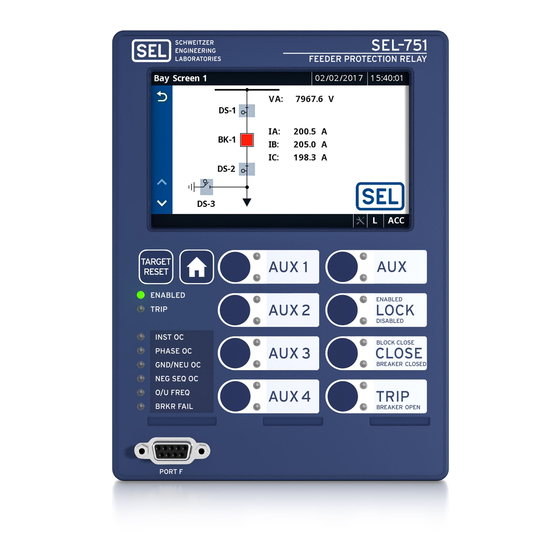
Feeder Protection Relay
Brand: Schweitzer Engineering Laboratories
|
Category: Relays
|
Size: 23.97 MB
Table of Contents
-
Overview25
-
Applications43
-
Definitions48
-
Overview57
-
Overview109
-
Setup110
-
Terminal111
-
Settings114
-
Event Analysis119
-
Overview127
-
Application Data129
-
Table157
-
Table163
-
Table164
-
Table165
-
Table166
-
Table181
-
Table200
-
Table207
-
Table209
-
Overview337
-
Load Profiling350
-
Breaker Monitor355
-
Overview367
-
Overview451
-
Table459
-
Figure466
-
Table472
-
Table477
-
Overview515
-
Overview559
-
Figure560
-
Figure567
-
Figure578
-
Overview583
-
Event Reporting584
-
Overview621
-
Self-Test633
-
-
Firmware639
-
-
ICD File646
-
Overview661
-
-
Overview685
-
-
Features777
-
-
-
Logical Nodes795
-
-
Overview829
-
Features842
-
Overview845
-
-
-
Date Code911
Advertisement
Advertisement
Related Products
- Schweitzer Engineering Laboratories SEL-787
- Schweitzer Engineering Laboratories SEL-700G Series
- Schweitzer Engineering Laboratories SEL-700G1
- Schweitzer Engineering Laboratories SEL-700GT
- Schweitzer Engineering Laboratories SEL-787-2
- Schweitzer Engineering Laboratories SEL-787-2E
- Schweitzer Engineering Laboratories SEL-787-4X
- Schweitzer Engineering Laboratories SEL-749M
- Schweitzer Engineering Laboratories SEL-787-3S
- Schweitzer Engineering Laboratories SEL-787-21