Sign In
Upload
Manuals
Brands
Lattice Semiconductor Manuals
Motherboard
ECP5-5G
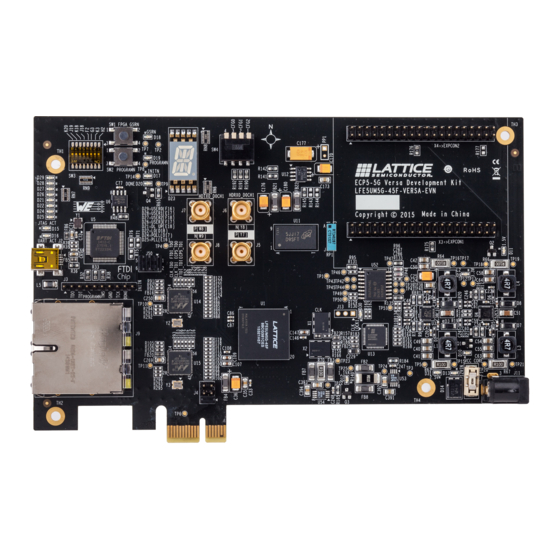
Lattice Semiconductor ECP5-5G Manuals
Manuals and User Guides for Lattice Semiconductor ECP5-5G. We have
4
Lattice Semiconductor ECP5-5G manuals available for free PDF download: Technical Note, Technical Notes, Usage Manual, User Manual
Lattice Semiconductor ECP5-5G Technical Note (86 pages)
High-Speed I/O Interface
Brand:
Lattice Semiconductor
| Category:
Recording Equipment
| Size: 3.15 MB
Table of Contents
Table of Contents
3
Acronyms in this Document
9
1 Introduction
10
2 External Interface Description
10
Figure 2.1. External Interface Definitions
10
3 High-Speed I/O Interface Building Blocks
11
Edge Clocks
11
Primary Clocks
11
DQS Lane
11
Figure 3.1. ECP5 and ECP5-5G Device Clocking Diagram
11
Pll
12
Ddrdll
12
Dqsbuf
12
Figure 3.2. DDRDLL Connectivity
12
Dlldel
13
Input DDR (IDDR)
13
Output DDR (ODDR)
13
Edge Clock Dividers (CLKDIV)
13
Input/Output DELAY
13
4 Building Generic High Speed Interfaces
14
Types of High-Speed DDR Interfaces
14
Table 4.1. Generic High-Speed I/O DDR Interfaces
14
5 High-Speed DDR Interface Details
15
Gddrx1_Rx.sclk.centered
15
Figure 5.1. Gddrx1_Rx.sclk.centered Interface (Static Delay)
15
Figure 5.2. Gddrx1_Rx.sclk.centered Interface (Dynamic Data Delay)
15
Gddrx1_Rx.sclk.aligned
16
Figure 5.3. Gddrx1_Rx.sclk.aligned Interface (Static Delay)
16
Gddrx2_Rx.eclk.centered
17
Figure 5.4. Gddrx1_Rx.sclk.aligned Interface (Dynamic Data/Clock Delay)
17
Gddrx2_Rx.eclk.aligned
18
Figure 5.5. Gddrx2_Rx.eclk.centered Interface (Static Delay)
18
Figure 5.6. Gddrx2_Rx.eclk.centered Interface (Dynamic Data Delay)
18
Figure 5.7. Gddrx2_Rx.eclk.aligned Interface (Static Delay)
19
Figure 5.8. Gddrx2_Rx.eclk.aligned Interface (Dynamic Data/Clock Delay)
19
Gddrx2_Rx.mipi
20
Figure 5.9. GDDRX2_RX.MIPI
20
Gddrx71_Rx.eclk
21
Figure 5.10. GDDRX71_RX.ECLK Interface
21
Gddrx1_Tx.sclk.aligned
22
Gddrx1_Tx.sclk.centered
22
Figure 5.11. Gddrx1_Tx.sclk.aligned Interface
22
Gddrx2_Tx.eclk.aligned
23
Figure 5.12. Gddrx1_Tx.sclk.centered Interface
23
Figure 5.13. Gddrx2_Tx.eclk.aligned Interface
23
Gddrx2_Tx.eclk.centered
24
Figure 5.14. Gddrx2_Tx.eclk.centered Interface
24
Gddrx71_Tx.eclk
25
Generic DDR Design Guidelines
25
Using the High Speed Edge Clock Bridge
25
Figure 5.15. GDDRX71_TX.ECLK Interface
25
Receive Interface Guidelines
26
Transmit Interface Guidelines
26
Clocking Guidelines for Generic DDR Interface
26
Timing Analysis for High Speed DDR Interfaces
27
Frequency Constraints
27
DDR Input Setup and Hold Time Constraints
27
Figure 5.16. RX Centered Interface Timing
27
DDR Clock to out Constraints for Transmit Interfaces
28
Figure 5.17. RX Aligned Interface Timing
28
Figure 5.18. Tco Min and Max Timing Analysis
29
Figure 5.19. Transmit Centered Interface Timing
29
Figure 5.20. Transmit Aligned Interface Timing
30
6 ECP5 and ECP5-5G Memory Interfaces
31
Figure 6.1. Typical DDR2/DDR3/DDR3L Memory Interface
31
Figure 6.2. Typical LPDDR2/LPDDR3 Memory Interface
32
Figure 6.3. DQ-DQS During Read
32
Figure 6.4. DQ-DQS During Write
32
DDR Memory Interface Requirements
33
Table 6.1. DDR Memory Configurations Support
33
Features for Memory Interface Implementation
34
DQS Grouping
34
Figure 6.5. DQ-DQS Grouping
34
DLL-Compensated DQS Delay Elements
35
Data Valid Module
35
Figure 6.6. DQSBUF Block Functions
35
Table 6.2. DDRDLL Connectivity
35
READ Pulse Positioning Optimization
36
Table 6.3. DDRDLL Connectivity
36
Figure 6.7. READ Signal Training Process
37
Dynamic Margin Control on DQSBUF
38
Read Data Clock Domain Transfer Using Input FIFO
38
DDR Input and Output Registers (IDDR/ODDR)
38
Memory Interface Implementation
38
Read Implementation
38
Figure 6.8. DDR2, DDR3/DDR3L, LPDDR2, and LPDDR3 Read Side Implementation
39
Write Implementation (DQ, DQS, and DM)
40
Figure 6.9. DDR2, DDR3/DDR3L, LPDDR2, and LPDDR3 Write Side (DQ, DQS, and DM)
40
Write Implementation (DDR2, DDR3/DDR3L Address, Command, and Clock)
41
Figure 6.10. DDR2, DDR3/DDR3L Address, Command, and Clock Generation
41
Write Implementation (LPDDR2 and LPDDR3 Address, Command, and Clock)
42
Figure 6.11. LPDDR2 Output for CA Generation
42
Figure 6.12. LPDDR2 Output for CSN, CKE, and CLOCK Generation
43
Figure 6.13. LPDDR3 Output Side for CA Generation
43
DDR Memory Interface Design Rules and Guidelines
44
Figure 6.14. LPDDR3 Output Side for CSN, CKE, ODT, and CLOCK Generation
44
DDR2/DDR3 Memory Interface Termination Guidelines
45
Termination for DQ, DQS, and DM
45
Termination for CK
45
Table 6.4. I/O Standards for DDR Memory
45
Termination for Address, Commands, and Controls
46
Termination for DDR3/DDR3L DIMM
46
DDR Memory Interface Pinout Guidelines
46
Pin Placement Considerations for Improved Noise Immunity
47
7 Using Clarity Designer to Build and Plan High Speed DDR Interfaces
49
Figure 7.1. Clarity Design Main Window
49
Configuring DDR Modules in Clarity Designer
50
Configuring SDR Modules
50
Figure 7.2. SDR Option Selected in the Catalog Tab of Clarity Designer
50
Figure 7.3. SDR Configuration Tab
51
Table 7.1. SDR Configuration Parameters
52
Configuring DDR Generic Modules
53
Figure 7.4. Ddr_Generic Option Selected in the Catalog Tab of Clarity Designer
53
Figure 7.5. Ddr_Generic Pre-Configuration Tab
53
Figure 7.6. Ddr_Generic Configuration Tab
54
Table 7.2. Ddr_Generic Pre-Configuration Parameters
54
Table 7.3. Ddr_Generic Configuration Tab Parameters
55
Table 7.4. Clarity Designer Ddr_Generic Interface Selection
56
Configuring 7:1 LVDS Interface Modules
57
Figure 7.7. GDDR_7:1 Option Selected in the Catalog Tab of Clarity Designer
57
Figure 7.8. GDDR_7:1 LVDS Configuration Tab
57
Configuring DDR Memory Interfaces
58
Figure 7.9. DDR_MEM Option Selected in the Catalog Tab of Clarity Designer
58
Table 7.5. GDDR_7:1 LVDS Configuration Parameters
58
Figure 7.10. DDR_MEM Configuration Tab
59
Table 7.6. DDR_MEM Configuration Tab Parameters
60
Figure 7.11. DDR_MEM Clock/Address/Command Tab
61
Table 7.7. DDR_MEM Clock/Address/Command Parameters
61
Building DDR Interfaces in Clarity Designer
62
Figure 7.12. DDR_MEM Advanced Settings Tab
62
Table 7.8. DDR_MEM Advanced Settings Tab Parameters
62
Planning DDR Interfaces in Clarity Designer
63
Figure 7.13. DDR Modules Paced Using Clarity Design Planner
63
8 DDR Software Primitives and Attributes
64
Input/Output DELAY
64
Table 8.1. Software Primitives
64
Delayf
65
Delayg
65
Figure 8.1. DELAYF Primitive
65
Figure 8.2. DELAYG Primitive
65
Table 8.2. DELAYF Port List
65
Table 8.3. DELAYG Port List
65
DELAY Attribute Description
66
DDRDLL (Master DLL)
66
Ddrdlla
66
Figure 8.3. DDRDLLA Primitive
66
Table 8.4. DELAYF and DELAYG Attributes
66
DLL Delay (DLLDEL)
67
Figure 8.4. DLLDELD Primitive
67
Table 8.5. DDRDLLA Port List
67
Table 8.6. DDRDLL Attributes
67
Table 8.7. DLLDELD Port List
67
Generic DDR Input and Output Primitives
68
Input DDR Primitives
68
Iddrx1F
68
Figure 8.5. IDDDRX1F Primitive
68
Table 8.8. DLLDELD Attributes
68
Table 8.9. IDDRX1F Port List
68
Iddrx2F
69
Iddr71B
69
Figure 8.6. IDDRX2F Primitive
69
Figure 8.7. IDDR71B
69
Table 8.10. IDDRX2F Port List
69
Table 8.11. IDDRX2F Port List
69
Output DDR Primitives
70
Oddrx1F
70
Oddrx2F
70
Figure 8.8. ODDRX1F
70
Figure 8.9. ODDRX2F
70
Table 8.12. ODDRX1F Port List
70
Table 8.13. ODDRX2F Port List
70
Oddr71B
71
Memory DDR Primitives
71
DQSBUF (DQS Strobe Control Block)
71
Figure 8.10. ODDR71B Primitive
71
Table 8.14. ODDR71B Port List
71
Dqsbufm
72
Figure 8.11. DQSBUFM Primitive
72
Table 8.15. DQSBUF Port List
72
Input and Output Memory DDR Primitives
73
Table 8.16. DQSBUFM Attributes
73
Table 8.17. Summary of All DDR Memory Primitives
73
Memory Input DDR Primitives
74
Iddrx2Dqa
74
Figure 8.12. IDDRX2DQA Primitive
74
Table 8.18. DQSBUF Port List
74
Table 8.19. Memory Primitive Attributes
74
Memory Output DDR Primitives for DQ Output
75
Oddrx2Dqa
75
Memory Output DDR Primitives for DQS Output
75
Oddrx2Dqsb
75
Figure 8.13. ODDRX2DQA
75
Figure 8.14. ODDRX2DQSB Primitive
75
Table 8.20. ODDRX2DQA Port List
75
Memory Output DDR Primitives for Tristate Output Control
76
Tshx2Dqa
76
Tshx2Dqsa
76
Figure 8.15. TSHX2DQA Primitive
76
Figure 8.16. TSHX2DQSA Primitive
76
Table 8.21. ODDRX2DQA Port List
76
Table 8.22. TSHX2DQA Port List
76
Memory Output DDR Primitives for Address and Command
77
Oshx2A
77
Figure 8.17. OSHX2A Primitive
77
Table 8.23. TSHX2DQSA Port List
77
Table 8.24. OSHX2A Port List
77
9 Soft IP Modules
78
Detailed Description of each Soft IP
78
Gddr_Sync
78
Figure 9.1. GDDR_SYNC Ports
78
Table 9.1. List of Soft Ips Supported
78
Table 9.2. Soft IP Used in each Interface
78
Rx_Sync
79
Figure 9.2. RX_SYNC Ports
79
Table 9.3. GDDR_SYNC Port List Description
79
Table 9.4. GDDR_SYNC Port List Description
79
Mem_Sync
80
Bw_Align
80
Figure 9.3. MEM_SYNC Ports
80
Figure 9.4. BW_ALIGN Ports
80
Table 9.5. MEM_SYNC Port Description
80
Mipi_Filter
81
Figure 9.5. MIPI_FILTER Ports
81
Table 9.6. BW_ALIGN Port Description
81
Table 9.7. MIPI_FILTER Port Description
82
Technical Support Assistance
83
Revision History
84
Advertisement
Lattice Semiconductor ECP5-5G Technical Notes (78 pages)
High-Speed I/O Interface
Brand:
Lattice Semiconductor
| Category:
Recording Equipment
| Size: 8.59 MB
Table of Contents
Interface Requirements
7
Plus, Minus
63
Set, Reset
69
Technical Support Assistance
78
Revision History
78
Lattice Semiconductor ECP5-5G User Manual (33 pages)
Brand:
Lattice Semiconductor
| Category:
Motherboard
| Size: 3.41 MB
Table of Contents
ECP5-5G Device
3
Applying Power to the Board
3
Programming/Fpga Configuration
4
Alternate Programmer Download Interface
4
Diamond Programmer Requirements
4
Setting the Configuration Mode
5
Board Programming
5
PROGRAMN and GSRN
7
Programming Serial SPI Flash Memory
7
On-Board Clock Capabilities
9
General Purpose Clock Source
10
FPGA Test Pins
11
General Purpose DIP Switches
11
General Purpose Leds
12
Alpha-Numeric LED Display
12
DDR3 Memory Device
13
Ethernet Interfaces
15
Ordering Information
17
Technical Support Assistance
17
Revision History
17
Appendix A. Schematics
18
Appendix B. Bill of Materials
28
Advertisement
Lattice Semiconductor ECP5-5G Usage Manual (43 pages)
Brand:
Lattice Semiconductor
| Category:
Computer Hardware
| Size: 4.95 MB
Table of Contents
Appendix A. Primary Clock Sources and Distribution Section
2
Clock Phase Adjustment
5
Frequency Synthesis
6
Additional Features
6
Functional Description
26
PLL Features
26
Technical Support Assistance
39
Revision History
39
Appendix B. Pinout Rules for Clocking in ECP5 and ECP5-5G Devices
43
Advertisement
Related Products
Lattice Semiconductor EVDK
Lattice Semiconductor ECP5 Versa
Lattice Semiconductor ASC Bridge Board
Lattice Semiconductor CrossLink LIF-MD6000
Lattice Semiconductor HDMI-VIP-IB-EVN
Lattice Semiconductor Himax HM01B0
Lattice Semiconductor iCE40 UltraLite
Lattice Semiconductor iCE40 UltraPlus
Lattice Semiconductor iCE40 UltraPlus Series
Lattice Semiconductor iCE40HX-8K
Lattice Semiconductor Categories
Motherboard
Computer Hardware
Microcontrollers
Controller
Recording Equipment
More Lattice Semiconductor Manuals
Login
Sign In
OR
Sign in with Facebook
Sign in with Google
Upload manual
Upload from disk
Upload from URL