Sign In
Upload
Manuals
Brands
Intel Manuals
Computer Hardware
Pentium 4
Intel Pentium 4 Manuals
Manuals and User Guides for Intel Pentium 4. We have
11
Intel Pentium 4 manuals available for free PDF download: Design Manual, User Manual, Datasheet, Specification, Installation Notes, Product Overview
Intel Pentium 4 Design Manual (371 pages)
in the 478-pin Package / Intel 850 Chipset Family Platform
Brand:
Intel
| Category:
Computer Hardware
| Size: 12.78 MB
Table of Contents
Table of Contents
3
Introduction
17
Related Documentation
18
Conventions and Terminology
19
Table 1. Platform Conventions and Terminology
19
System Overview
21
Intel ® Pentium ® 4 Processor in the 478-Pin Package
21
Chipset
21
Intel 82850/82850E Memory Controller Hub (MCH)
22
Ich2
22
System Configurations
23
Figure 1.Typical System Configuration
23
Platform Initiatives
24
Intel ® 850 Chipset
24
Rambus Direct RDRAM* Device Interface
24
Accelerated Graphics Port (AGP)
24
Ich2
24
Integrated LAN Controller
24
Intel ® AC'97 6-Channel Support
25
Table 2. Intel ® ICH2 Codec Options
25
Low Pin Count (LPC) Interface
26
Ultra ATA
26
Universal Serial Bus (USB)
26
Platform Manageability
27
PC '99/'01 Platform Compliance
28
Component Quadrant Layout
29
Processor Component Quadrant Layout
29
Figure 2. Processor Socket Quadrant Layout
29
Intel ® 850/850E Chipset Component Quadrant Layout
30
Figure 3. Intel ® 850/850E Chipset Quadrant Layout
30
Figure 4. Intel ® ICH2 Quadrant Layout
30
Platform Placement and Stack-Up Overview
31
Platform Component Placement
31
Six-Layer Motherboard
31
Table 3. Placement Assumptions for the Desktop Configuration (6-Layer Motherboard)
31
Four-Layer Motherboard
32
Figure 5. Desktop Component Placement Example (6-Layer Motherboard)
32
Table 4. Placement Assumptions for the Desktop Configuration (4-Layer Motherboard)
32
Figure 6. Desktop Component Placement Example (4-Layer Motherboard)
33
Four-Layer Motherboard Routing Strategy
34
Figure 7. Four-Layer Routing Strategy
35
Motherboard Layer Stack-Up
36
Six-Layer Motherboard Stack-Up
36
Figure 8. Six Layer Stack-Up
36
Design Considerations
37
Figure 9. Example Stack-Up for 6-Layer ATX Form Factor
37
Four-Layer Motherboard Stack-Up
38
Figure 10. 4-Layer Intel ® Pentium
38
Platform Clock Routing Guidelines
39
Figure 11. Clocking Architecture Using the CK00
40
Figure 12. Processor BCLK Topology
41
Routing Guidelines for System Bus Clocks
41
Figure 13. Source Shunt Termination
42
Table 5. BCLK [1:0] Routing Guidelines
43
Figure 14. Clock Skew as Measured from Agent to Agent
45
Figure 15. Trace Spacing
45
BCLK[1:0] Frequency Select
46
100 Mhz Operation - Intel 82850 Chipset
46
Figure 16. BCLK[1:0] Frequency Select for 100 Mhz System Bus Operation
46
133 Mhz Operation - Intel 82850E Chipset
47
Figure 17. BCLK [1:0] Frequency Select for 133 Mhz System Bus Operation
47
CK00 to Rambus DRCG* (Reference Clocks)
48
Figure 18. Vddir and 3Vmref Routing
48
Routing Guidelines for Rambus RDRAM* Device Clocks
48
Intel ® MCH to Rambus DRCG* (Phase Aligning Clocks)
49
Rambus DRCG* to Direct Rambus Channels (400 Mhz Clocks)
49
Figure 19. Intel ® MCH to Rambus DRCG* Routing
49
Figure 20. Rambus RDRAM* Device Clock Routing Dimension
50
Table 6. Rambus RDRAM* Device Clock Routing Guidelines
50
Trace Lengths
50
Figure 21. Differential Clock Routing
51
Figure 22. Non-Differential Clock Routing
52
Rambus RDRAM* Device Clocktermination
52
Topology Considerations
52
Figure 23. CFM/CFM# Termination - 300/400 Mhz Rambus RDRAM* Technology
53
Figure 24. CFM/CFM# Termination - 533 Mhz Rambus RDRAM* Technology
53
Rambus DRCG* Impedance Matching Circuit
54
Figure 25. Rambus DRCG* Impedance Matching Network
54
Table 7. Rambus DRCG* Impedance Matching Network Values
54
Rambus DRCG* Layout Example
55
Figure 26. Rambus DRCG* Layout Example
55
Routing Guidelines for 66 Mhz and 33 Mhz Clocks
56
66 Mhz / 33 Mhz Clock Relationships
56
Figure 27. 66 Mhz / 33 Mhz Clock Relationships
56
66 Mhz Clock Routing Length Guidelines
57
3V66 Clock Routing Requirement for Intel
57
82850E Platforms
57
Figure 28. AGP_66 Clock Routing Topology
57
Figure 29. CLK_66 Clock Routing Topology
57
Table 8. 66 Mhz Clock Routing Length Guidelines
57
33 Mhz Clock Routing Length Guidelines
58
Figure 30. PCI_33 Clock Routing Topology
58
Table 9. 33 Mhz Clock Routing Guidelines
58
Figure 31. CLK_33 Clock Routing Topology
59
System Bus Routing
61
Table 10. System Bus Routing Summary for the Processor
61
Return Path
62
Figure 32. GTLREF Routing
63
GTLREF Layout and Routing Recommendations
63
Processor Configuration
64
Topology and Routing
64
Table 11. Source Synchronous Signal Groups and the Associated Strobes
64
Design Recommendations
65
Design Considerations
66
Figure 33. Processor Topology
66
Table 12. Processor Package Lengths
66
Routing Guidelines for Asynchronous GTL+ and Other Signals
71
Table 13. Miscellaneous Signals (Signals that Are Not Data, Address, or Strobe)
71
Topologies
72
Figure 34. Routing Illustration for FERR
72
Table 14. Layout Recommendations for FERR# Signals (Topology 1A)
72
Topology 1: Asynchronous GTL+ Signals Driven by the Processor
72
Figure 35. Routing Illustration for PROCHOT# and THERMTRIP# (Topology 1B)
73
Figure 36. Routing Illustration for A20M#, IGNNE#, LINT[1:0], SLP#, SMI#, and
73
Ich2
73
Table 15. Layout Recommendations for PROCHOT# and THERMTRIP# Signals (Topology 1B)
73
Table 16. Layout Recommendations for Miscellaneous Signals (Topology 2)
73
Topology 2: Asynchronous GTL+ Signals Driven by Intel
73
Figure 37. Routing Illustration for INIT
74
Figure 38. Voltage Translation of INIT
74
Table 17. Layout Recommendations for INIT# (Topology 2A)
74
Topology 2A: INIT
74
Figure 39. Routing Illustration for PWRGOOD
75
Figure 40. Routing Illustration for VCCIOPLL, VCCA and VSSA
75
Ich2
75
Table 18. Layout Recommendations for Miscellaneous Signals (Topology 2B)
75
Topology 2B: Asynchronous GTL+ Signals Driven by Intel
75
Topology 3: VCCIOPLL, VCCA and VSSA
75
Figure 41. Routing Illustration for BR0# and RESET
76
Table 19: BR0# and RESET# Lengths
76
Topology 4: BR0# and RESET
76
Topology 5: COMP[1:0] Signals
76
Topology 6A: BSEL[1:0] Termination - 400 Mhz System Bus Only
76
Topology 6B: BSEL[1:0] Termination - 533/400 Mhz System Bus
76
Topology 7: THERMDA/THERMDC Routing Guidelines
77
Topology 8: TESTHI and RESERVED Pins
77
Topology 9: Processor Voltage Regulator Sequencing Requirements
78
VCCVID Regulator Recommendations
78
Figure 42. Passing Monotonic Rising Edge Voltage Waveform
79
Figure 43. Failing Non-Monotonic Rising Voltage Waveform
79
Figure 44. THERMTRIP# Power down Circuit
80
Figure 45. Power Sequencing Block Diagram
80
Topology 10: THERMTRIP# Power down Circuit
80
Figure 46: Power-On Sequence Timing Diagram
81
Figure 47. Power-Off Sequence Timing Diagram
81
Figure 48. THERMTRIP# Power down Sequence
82
Figure 49. Voltage Divider Network for Reference Voltage Generation
82
Intel ® MCH System Bus Interface
82
Figure 50. Pull-Down Circuit
83
Intel ® MCH System Bus I/O Decoupling Requirements
83
Table 20. Reference Voltage Network Values
83
Figure 51. Example Intel ® MCH Decoupling Guidelines for Chipset
84
Figure 52. Customer Reference Platform System Bus Routing - Top Layer
85
Figure 53, Customer Reference Platform System Bus Routing - Bottom Layer
86
Figure 54. Processor Power Delivery on Layer 2
87
Processor Power Delivery
87
Figure 55. Processor Power Delivery on Layer 4
88
System Bus Routing Guidelines - Four-Layer Motherboard
85
Memory Interface Routing
89
Rambus RDRAM* Device Routing Guidelines
90
Figure 56. Intel ® MCH Direct Rambus Channel Routing Example
90
Rambus Signaling Level (RSL) Signals
91
Table 21. Direct Rambus Channel Signal Groups
91
Figure 57. Example Direct Rambus Channel Routing
92
Table 22. Direct Rambus RSL Signal Lengths for Rambus RIMM* Connectors on
92
Figure 58. RSL Routing Diagram Showing Ground Isolation Traces with VIA Around RSL Signals
93
Rambus* Signaling Level (RSL) Channel Compensation
94
Figure 59. Direct Rambus Channel Trace Length Matching Example
94
Package Trace Compensation (RSL and Clocking Signals)94
94
Via Compensation
95
Differential Clock Compensation
96
Figure 60. "Dummy" Vs. "Real" Vias
96
Non-Differentially Routed Clocks - 533 Mhz Rambus RDRAM* Technology
97
Figure 61. RSL and Clocking Signal Layer Alteration
98
Rambus RIMM Connector Impedance Compensation
98
Signal Layer Alternation for Rambus RIMM Connector Pin Compensation
98
Table 23. RSL and Clocking Signal Rambus RIMM* Connector Capacitance Requirement
99
Figure 62. Top Layer CTAB with RSL Signal Routed on the same Layer (Ceff = 0.8
100
Table 24. Copper Tab Area Calculation
100
Figure 63. Bottom Layer CTAB with RSL Signal Routed on the same Layer
101
Figure 64. Bottom Layer Ctabs Split Across the Top and Bottom Layer to Achieve an
101
Figure 65. Direct Rambus RDRAM* Device Termination (Discrete Resistors Are Recommended)
102
RSL Signal Termination
102
Figure 66. Direct Rambus RDRAM* Device Termination Example
103
Figure 67. RAMREF Generation Example Circuit for 300/400 Mhz Rambus RDRAM
104
Figure 68. RAMREF Generation Example Circuit for 533 Mhz Rambus RDRAM
104
Rambus RDRAM* Device Reference Voltage
104
Figure 69. High-Speed CMOS RC Termination
105
High-Speed CMOS Routing
105
SIO Routing
105
Figure 70. SIO Routing
106
Suspend-To-RAM Shunt Transistor
107
Figure 71. Rambus RDRAM* Device CMOS Shunt Transistor
108
Rambus RDRAM* Device Channel Margin Improvement
108
533 Mhz (PC1066) Rambus RIMM Module Thermal Consideration
109
Rambus Technology Routing Guidelines - Four-Layer Motherboard
110
Figure 72. Rambus RIMM Connector Placement
110
Figure 73. Rambus Technology Intel
111
Figure 74. Rambus Technology Intel
112
Optimized Rambus RDRAM* Device Routing Rules for a Four-Layer Motherboard Design
112
AGP Interface Routing
113
Table 25. AGP 2.0 Signal Groups
113
AGP Routing Guidelines
114
Timing Domain Signal Routing Guidelines
114
4X Timing Domain Signal Routing Guidelines
114
Trace Lengths Less than 6 Inches
114
Figure 75. AGP 2X/4X Routing Example for Interfaces < 6 Inches
115
Trace Lengths Greater than 6 Inches and Less than 7.25 Inches
115
AGP Interfaces Trace Length Summary
116
Table 26. AGP 2.0 Routing Summary
116
I/O Decoupling Guidelines
117
Figure 76. AGP I/O Decoupling Example with a VSS Flood to Improve Power Delivery to the Intel ® MCH
117
Signal Power/Ground Referencing Recommendations
118
VDDQ and TYPEDET
118
VREF Generation
118
MCH AGP Interface Buffer Compensation
119
AGP Pull-Ups/Pull-Down on AGP Signals
119
Figure 77. AGP 2.0 VREF
119
Table 27. AGP Pull-Up/Pull-Down Resistors
120
AGP Signal Voltage Tolerance List
121
AGP Connector
121
AGP Universal Retention Mechanism (RM)
121
Table 28. 3.3 V and 5 V Tolerant Signals During 1.5 V Operation
121
Figure 78. AGP Left Handed Retention Mechanism Drawing
122
Figure 79. AGP Left Handed Retention Mechanism Keep-Out Information
123
Table 29 List of Vendors for Retention Mechanism
123
AGP Routing Guidelines - Four-Layer Motherboard
124
Figure 80. Example AGP Routing (Top Layer)
124
Figure 81. Example AGP Routing (Bottom Layer)
125
Figure 82. Example VDDQ Plane on Layer 2
126
Hub Interface Routing
127
Hub Interface Routing Guidelines
127
Figure 83. 8-Bit Hub Interface Routing Example
127
8-Bit Hub Interface Routing Guidelines
128
8-Bit Hub Interface Data Signals
128
8-Bit Hub Interface Strobe Signals
128
8-Bit Hub Interface HIREF Generation/Distribution
128
Table 30. 8-Bit Hub Interface Buffer Configuration Setting
128
Table 31. 8-Bit Hub Interface HUBREF Generation Circuit Specifications
128
Figure 84. 8-Bit Hub Interface with a Shared Reference Divider Circuit (Normal Mode)
129
Figure 85. 8-Bit Hub Interface with Locally Generated Reference Divider Circuits
129
8-Bit Hub Interface Compensation
130
8-Bit Hub Interface Decoupling Guidelines
130
Table 32. 8-Bit Hub Interface RCOMP Resistor Values
130
Hub Interface Routing Guidelines - Four-Layer Motherboard
131
Figure 86. Example Hub Interface Breakout / 1.8 V MCH Fingers
131
I/O Controller Hub 2
133
This Chapter Provides Information on the Intel 82801BA I/O Controller Hub 2 (ICH2) IDE Interface
133
IDE Cable
133
Cable Detection for Ultra ATA/66 and Ultra ATA/100
134
Combination Host-Side/Device-Side Cable Detection
135
Figure 87. Combination Host-Side/Device-Side IDE Cable Detection
135
Device-Side Cable Detection
136
Figure 88. Device-Side IDE Cable Detection
136
Primary IDE Connector Requirements
137
Figure 89. Connection Requirements for Primary IDE Connector
137
Secondary IDE Connector Requirements
138
Figure 90. Connection Requirements for Secondary IDE Connector
138
Communication and Networking Riser (CNR)
139
CNR Placement
139
Figure 91. CNR Interface
139
Intel ® AC'97
140
Figure 92. Intel ® ICH2 AC'97 - Codec Connection
140
Table 54. Intel
140
Table 55. Intel
140
Figure 93. Audio Codec
141
Figure 94. Modem Codec
141
Figure 95. Audio/Modem Codec
141
Figure 96. Modem Codecs
142
Figure 97. Audio and Modem Codecs
142
Figure 98. Audio Codecs
143
Figure 99. Audio and Audio/Modem Codecs
143
AC'97 Audio Codec Detect Circuit and Configuration Options
144
Table 33. Intel ® AC'97 SDIN Pull-Down Resistors
144
Figure 100. CDC_DN_ENAB# Support Circuitry for a Single Codec Motherboard
145
Figure 101. CDC_DN_ENAB# Support Circuitry for Multi-Channel Audio Upgrade
146
Figure 102. CDC_DN_ENAB# Support Circuitry for Two-Codecs on Motherboard / One-Codec on CNR
146
Figure 103. CDC_DN_ENAB# Support for Two-Codecs on Motherboard / Two-Codecs on CNR
147
Table 34. Signal Descriptions
147
Valid Codec Configurations
148
USB Guidelines
148
Table 35. Codec Configurations
148
IOAPIC Design Recommendations
149
Figure 104. USB Data Signals
149
Smbus/Smlink Interface
150
Figure 105. Smbus/Smlink Interface
150
Smbus Architecture and Design Considerations
151
General Design Issues / Notes
151
Smbus Design Considerations
151
Figure 106. Unified Vcc_Suspend Architecture
152
Figure 107. Unified Vcc_Core Architecture
152
The Unified VCC_ Suspend Architecture
152
The Unified Vcc_Core Architecture
152
Mixed Architecture
153
Pci
153
Figure 108. Mixed Vcc_Suspend/Vcc_Core Architecture
153
Figure 109. PCI Bus Layout Example
153
Figure 110. Example PCI Power Planes on Layer 2
154
PCI Routing - Four-Layer Motherboard
154
Figure 111. Example PCI Routing on Layer 1
155
Figure 112. Example PCI Routing on Layer 4
156
Rtc
157
RTC Crystal
157
Figure 113. External Circuitry for the Intel
157
External Capacitors
158
RTC Layout Considerations
158
RTC External Battery Connection
158
RTC External RTCRST Circuit
159
Figure 114. Diode Circuit to Connect RTC External Battery
159
RTC Routing Guidelines
160
VBIAS DC Voltage and Noise Measurements
160
Figure 115. RTCRST External Circuit for the Intel
160
Power-Well Isolation Control
161
Figure 116. RTC Power-Well Isolation Control
161
Power Supply PS_ON Consideration
162
LAN Layout Guidelines
162
Table 36. Integrated LAN Options
162
Figure 117. Intel ® ICH2 / LAN Connect Section
163
Table 37. LAN Design Guide Section Reference
163
Intel ® ICH2 - LAN Interconnect Guidelines
164
Bus Topologies
164
Figure 118. Single Solution Interconnect
164
Point-To-Point Interconnect
164
Figure 119. LOM/CNR Interconnect
165
LOM/CNR Interconnect
165
Table 38. Length Requirements for Single Solution Interconnect
165
Table 39. Length Requirements for LOM/CNR Interconnect
165
Crosstalk Considerations
166
Figure 120. LAN_CLK Routing Example
166
Impedances
166
Signal Routing and Layout
166
Line Termination
167
General LAN Routing Guidelines and Considerations
167
General Trace Routing Considerations
167
Figure 121. Trace Routing
168
Signal Isolation
168
Trace Geometry and Length
168
Figure 122. Ground Plane Separation
169
General Power and Ground Plane Considerations
169
Power and Ground Connections
169
Common Physical Layout Issues
170
Intel ® 82562EH Home/Pna* Guidelines
172
Crystals and Oscillators
172
Guidelines for Intel ® 82562EH Component Placement
172
Power and Ground Connections
172
Figure 123. Intel ® 82562 EH Termination
173
Phoneline HPNA Termination
173
Critical Dimensions
174
Distance from Intel ® 82562EH to Magnetics Module
174
Distance from Magnetics Module to Line RJ11
174
Figure 124. Critical Dimensions for Component Placement
174
Table 40. Critical Dimension Values
174
Distance from LPF to Phone RJ11
175
Intel ® 82562ET / 82562EM Guidelines
175
Guidelines for Intel ® 82562ET / 82562EM Component Placement
175
Critical Dimensions
176
Crystals and Oscillators
176
Figure 125. Intel ® 82562ET/ 82562EM Termination
176
Intel ® 82562ET / 82562EM Termination Resistors
176
Distance from Magnetics Module to RJ45
177
Figure 126. Critical Dimensions for Component Placement
177
Table 41. Critical Dimension Values
177
Distance from Intel 82562ET to Magnetics Module
178
Reducing Circuit Inductance
178
Terminating Unused Connections
178
Figure 127. Termination Plane
179
Termination Plane Capacitance
179
Figure 128. Intel ® 82562ET/EM Disable Circuit
180
Intel ® 82562 ET/EM Disable Guidelines
180
82562ET / 82562EH Dual Footprint Guidelines
181
Figure 129. Dual Footprint LAN Connect Interface
181
Figure 130. Dual Footprint Analog Interface
181
Intel ® ICH2 Routing Guidelines - Four-Layer Motherboard
183
Figure 131. Example Intel ® ICH2 Top Layer Breakout Using Standard Size Vias
183
Figure 132. Example Intel ® ICH2 Bottom Layer Breakout Using Standard Size Vias
184
FWH Guidelines
185
FWH Decoupling
185
In Circuit FWH Programming
185
FWH Vpp Design Guidelines
185
Figure 133. FWH VPP Isolation Circuitry
185
Intel ® ICH2 Decoupling Recommendations
186
Glue Chip 4 (Intel ICH2 Glue Chip)
186
Table 42. Decoupling Capacitor Recommendation
186
SPKR Pin Consideration
187
Figure 134. SPKR Circuit
187
1.8 V and 3.3 V Power Sequence Requirement
188
Figure 135. Example Power-On 3.3 V / 1.8 V Sequencing Circuit
188
PIRQ Routing
189
Figure 136. Example PCI IRQ Routing
189
Table 43. IOAPIC Interrupt Inputs 16 through 23 Usage
189
Additional Design Considerations
191
Retention Mechanism Placement and Keepouts
191
Figure 137. RM Keepout Drawing 1
192
Figure 138. RM Keepout Drawing 2
193
Figure 139. Intel ® MCH Keepouts and RM Hole Locations
194
Power Header for Active Cooling Solutions
195
Table 44. Reference Solution Fan Power Header Pinout
195
Table 45. Boxed Processor Fan Power Header Pinout
195
Intel ® Pentium
197
Intel® Pentium® 4 Processor in the 478-Pin Package Processor Power Distribution Guidelines
197
Power Requirements
197
FMB1 VR Component Placement
198
Figure 140. FMB1 VR Component Placement
198
FMB2 VR Component Placement
199
Figure 141. Four-Phase VR Component Placement
199
Figure 142. Three-Phase VR Component Placement
199
FMB1 Decoupling Requirements
200
Table 46. Decoupling Requirements
200
Table 47. Decoupling Locations
200
Figure 143. Decoupling Placement
201
FMB2 Decoupling Requirements
202
Table 48. Four-Phase Decoupling Requirements
202
Table 49. Three-Phase Decoupling Requirements
202
Table 50. Four-Phase Decoupling Locations
202
Figure 144. Four-Phase Decoupling Placement
203
Table 51. Three-Phase Decoupling Locations
203
Figure 145. Three-Phase Decoupling Placement
204
FMB1 Layout (6-Layer Board)
205
Figure 146. Top Layer Power Delivery Shape (VCC_CPU)
205
Figure 147. Layer 2 Power Delivery Shape (VSS)
206
Figure 148. Layer 3 Power Delivery Shape (VCC_CPU and VSS)
207
Figure 149. Layer 4 Power Delivery Shape (VCC_CPU and VSS)
208
Figure 150. Layer 5 Power Delivery Shape (VSS)
209
Figure 151. Bottom Layer Power Delivery Shape (VCC_CPU)
210
Figure 152. Alternating VCC_CPU/VSS Capacitor Placement
211
FMB2 Four-Phase Layout (4-Layer Board)
212
Figure 153. Top Layer Power Delivery Shape (VCC_CPU)
212
Figure 154. Layer 2 Power Delivery Shape (VSS)
213
Figure 155. Layer 3 Power Delivery Shape (VSS)
213
FMB2 - Three-Phase Layout (4-Layer Board)
214
Figure 156. Bottom Layer Power Delivery Shape (VCC_CPU)
214
Figure 157. Top Layer Power Delivery Shape (VCC_CPU)
215
Figure 158. Layer 2 Power Delivery Shape (Vss)
215
Figure 159. Layer 3 Power Delivery Shape (Vss)
216
Figure 160. Bottom Layer Power Delivery Shape (VCC_CPU)
216
FMB1 - Common Layout Issues
217
Figure 161. Shared Power and Ground Vias
217
Figure 162. Routing of VR Feedback Signal
218
FMB2 - Common Layout Issues
219
Figure 163. Shared Power and Ground Vias
219
Thermal Considerations
220
Fmb1
220
Fmb2
220
Figure 164. Routing of VR Feedback Signal
220
FMB2 - Voltage Regulator Thermal Protection Circuit
221
Table 52. Airflow Requirements
221
Figure 165. Example Circuit that Can be Used as a Thermal Monitor
222
Simulation
223
Fmb1
223
Figure 166. Detailed Power Distribution Model for Processor with Voltage Regulator on
223
Table 53. Intel ® Pentium ® 4 Processor Power Delivery Model Parameters
223
Fmb2
224
Figure 167. Detailed Power Distribution Model for Processor with Voltage Regulator on System Board
224
Filter Specifications for VCCA, VCCIOPLL, and VSSA
225
Figure 168. Typical VCCIOPLL, VCCA and VSSA Power Distribution
225
Figure 169. Filter Recommendation
226
Figure 170. Example Component Placement for PLL Filter
227
Power Distribution Guidelines
229
Definitions
229
Power Management
229
ACPI Hardware Model
230
Thermal Design Power
230
Figure 171. Global System Power States and Transition
230
1.8 V RAC Isolation Solution
231
Figure 172. Inductor-Capacitor Filter Circuit
231
Figure 173. Ferrite Bead Filter Circuit
232
Figure 174. Customer Reference Board Layout Example
233
Figure 175. Customer Reference Board Layout Example (Bottom - Layer 6)
233
Vterm/VDD Power Sequencing Requirement
234
Figure 176. Customer Reference Board Layout Example (Signal 2 - Layer 4)
234
Figure 177. 1.8 V and 2.5 V Power Sequence (Schottky Diode)
234
Intel ® 850 Chipset Power Sequencing Requirements
235
Figure 178. Desired Mode of Power Sequencing
235
Figure 179. Optional Mode of Power Sequencing
235
Intel ® ICH2 V5REF and Vcc3.3 Sequencing Requirement
236
Figure 180. V5REF Sequencing Circuit
236
CPU / CK00 Power Sequencing Requirement
237
Figure 181. CPU/CK00 Sequencing Circuit
237
Debug Port Routing Guidelines
239
Debug Tools Specifications
241
Logic Analyzer Interface (LAI)
241
Mechanical Considerations
241
Electrical Considerations
241
Schematic Review Checklist
243
Processor Checklist (All Signals)
243
CK00 Clock Generator Checklist
248
Direct Rambus Clock Generator (DRCG1 and DRCG2) Checklist
249
Intel ® 850 Chipset Checklist
251
AGP Checklist
253
Rambus RIMM* Connector Checklist
255
Intel ® ICH2 Checklist
259
PCI Interface
259
Hub Interface
260
LAN* Interface
260
EEPROM Interface
260
FWH/LPC Interface
261
Interrupt Interface
261
Gpio
262
Usb
263
Power Management
263
Processor Signals
263
System Management
264
Rtc
264
Miscellaneous Signals
265
Power
266
IDE Interface
267
Layout Review Checklist
269
Processor and System Bus
269
AGTL+ Signals
269
Asynchronous GTL+ and Other Signals
271
Processor Keep-Out Zones
271
Processor Decoupling
272
Intel ® 82850 MCH Decoupling
272
AGTL+ ( VREF HDVREF [3:0], HAVREF [1:0] and CCVREF)
273
CK00 Routing Guidelines
274
CK00 Clocking
274
RAMBUS Technology Routing Guidelines
276
RSL Signals
276
Ground Isolation
278
Layout
279
Rambus DRCG* Clock Routing Recommendation
280
Rambus DRCG* Layout (Clean Power Supply)
281
Rambus DRCG* (CTM/CTM# Output Network Layout)
282
RAMREF Routing
282
AGP Guidelines
282
All 1X Signals
282
2X/4X Signals
283
AGP Less than 6 Inches
283
AGP Interface Greater than 6 Inches and Less than 7.25 Inches
284
Intel ® MCH AGP Decoupling
284
AGP Connector Decoupling
285
Bit Hub Interface
285
Hub Decoupling
285
IDE Interface
286
Cnr
286
Intel ® AC'97
286
Usb
287
Intel ® ICH2 Decoupling
287
Rtc
288
LAN* Connect Interface
288
Miscellaneous
289
Advertisement
Intel Pentium 4 User Manual (105 pages)
User Guide
Brand:
Intel
| Category:
Computer Hardware
| Size: 5.42 MB
Table of Contents
Table of Contents
3
Revision History
8
1 Introduction
9
Document Goals and Scope
9
Importance of Thermal Management
9
Document Goals
9
Document Scope
10
References
11
Definition of Terms
12
2 Processor Thermal/Mechanical Information
15
Mechanical Requirements
15
Processor Package
15
Figure 1. Package IHS Load Areas
15
Heatsink Attach
17
General Guidelines
17
Heatsink Clip Load Requirement
17
Additional Guidelines
18
Thermal Requirements
18
Processor Case Temperature
18
Thermal Profile
19
Figure 2. Processor Case Temperature Measurement Location
19
Tcontrol
20
Figure 3. Example Thermal Profile
20
Heatsink Design Considerations
21
Heatsink Size
22
Heatsink Mass
22
Package IHS Flatness
22
Thermal Interface Material
23
System Thermal Solution Considerations
23
Chassis Thermal Design Capabilities
23
Improving Chassis Thermal Performance
23
Summary
24
System Integration Considerations
24
3 Thermal Metrology
25
Characterizing Cooling Performance Requirements
25
Example
26
Figure 4. Processor Thermal Characterization Parameter Relationships
26
Processor Thermal Solution Performance Assessment
27
Local Ambient Temperature Measurement Guidelines
27
Figure 5. Locations for Measuring Local Ambient Temperature, Active Heatsink
29
Figure 6. Locations for Measuring Local Ambient Temperature, Passive Heatsink
29
Processor Case Temperature Measurement Guidelines
30
4 Thermal Management Logic and Thermal Monitor Feature
31
Processor Power Dissipation
31
Thermal Monitor Implementation
31
PROCHOT# Signal
32
Thermal Control Circuit
32
Operation and Configuration
33
Figure 7. Concept for Clocks under Thermal Monitor Control
33
On-Demand Mode
34
System Considerations
34
Operating System and Application Software Considerations
35
On-Die Thermal Diode
35
Reading the On-Die Thermal Diode Interface
35
Table 1. Thermal Diode Interface
35
Correction Factors for the On-Die Thermal Diode
36
THERMTRIP# Signal
37
Cooling System Failure Warning
37
5 Intel ® Thermal/Mechanical Reference Design Information
39
Intel Validation Criteria for the Reference Design
39
Heatsink Performance Target
39
Table 2. ATX Reference Heatsink Performance Target
39
Acoustics
40
Altitude
40
Reference Heatsink Thermal Validation
41
Fan Performance for Active Heatsink Thermal Solution
41
Table 3. Fan Electrical Performance Requirements
41
Environmental Reliability Testing
42
Structural Reliability Testing
42
Figure 8. Random Vibration PSD
42
Random Vibration Test Procedure
42
Shock Test Procedure
42
Figure 9. Shock Acceleration Curve
43
Post-Test Pass Criteria
43
Recommended Test Sequence
43
Power Cycling
44
Recommended Bios/Processor/Memory Test Procedures
44
Material and Recycling Requirements
44
Safety Requirements
45
Geometric Envelope for ATX Intel ® Reference Thermal Mechanical Design
45
ATX Reference Thermal Mechanical Solution for the Intel Pentium 4 Processor in the 775-Land LGA Package
46
Figure 10. Intel ® RCBFH-3 Reference Design
46
Table 4. Intel ® RCBFH-3 Reference Design Performance
46
Figure 11. Intel RCBFH-3 Reference Design (Exploded View)
47
Reference Attach Mechanism
48
Structural Design Strategy
48
Figure 12. Upward Board Deflection During Shock
48
Mechanical Interface to the Reference Attach Mechanism
49
Figure 13. Reference Clip/Heatsink Assembly
49
Figure 14. Critical Parameters for Interfacing to Reference Clip
51
Figure 15. Critical Core Dimension
51
6 Acoustic Fan Speed Control
53
Thermal Solution Design
53
Compliance to Thermal Profile
53
Determine Thermistor Set Points
53
Minimum Fan Speed Set Point
54
Figure 16. Thermistor Set Points
54
Board and System Implementation
55
Choosing Fan Speed Control Settings
55
Figure 17. Example Acoustic Fan Speed Control Implementation
55
Figure 18. Fan Speed Control
56
Temperature to Begin Fan Acceleration
56
Figure 19. Temperature Range = 5 °C
57
Figure 20. Temperature Range = 10 °C
58
Minimum PWM Duty Cycle
58
Combining Thermistor and Thermal Diode Control
59
Interaction of Thermal Profile and T
59
Figure 21. Diode and Thermistor
59
Appendix Alga775 Socket Heatsink Loading
61
LGA775 Socket Heatsink Considerations
61
Metric for Heatsink Preload for Atx/Μatx Designs Non-Compliant with Intel Reference Design
61
Heatsink Preload Requirement Limitations
61
Motherboard Deflection Metric Definition
62
Table 5. Board Deflection Configuration Definitions
62
Board Deflection Limits
63
Figure 22. Board Deflection Definition
63
Board Deflection Metric Implementation Example
64
Figure 23. Example: Defining Heatsink Preload Meeting Board Deflection Limit
64
Additional Considerations
65
A.2.5 Additional Considerations
65
Motherboard Stiffening Considerations
65
Heatsink Selection Guidelines
66
Appendix B Heatsink Clip Load Metrology
67
Overview
67
Test Preparation
67
Heatsink Preparation
67
B.1 Overview
67
B.2 Test Preparation
67
B.2.1 Heatsink Preparation
67
Figure 24. Load Cell Installation in Machined Heatsink Base Pocket (Bottom View)
68
Figure 25. Load Cell Installation in Machined Heatsink Base Pocket (Side View)
69
Figure 26. Preload Test Configuration
69
Typical Test Equipment
70
Test Procedure Examples
70
Table 6. Typical Test Equipment
70
Preload Degradation under Bake Conditions
71
Time-Zero, Room Temperature Preload Measurement
71
Appendix C Thermal Interface Management
73
Bond Line Management
73
Interface Material Area
73
Interface Material Performance
73
Appendix D Case Temperature Reference Metrology
75
Objective and Scope
75
Definitions
75
D.2 Definitions
75
Supporting Test Equipment
76
Thermal Calibration and Controls
77
IHS Groove
77
D.5 IHS Groove
77
Figure 27. 775-Land LGA Package Reference Groove Drawing
78
Figure 28. IHS Reference Groove on the 775-Land LGA Package
79
Figure 29. IHS Groove Orientation Relative to the LGA775 Socket
79
Thermocouple Attach Procedure
80
Thermocouple Conditioning and Preparation
80
Thermocouple Attachment to the IHS
80
Figure 30. Bending the Tip of the Thermocouple
80
Figure 31. Securing Thermocouple Wires with Kapton Tape Prior to Attach
81
Figure 32. Thermocouple Bead Placement
81
Figure 33. Position Bead on the Groove Step
82
Figure 34. Detailed Thermocouple Bead Placement
82
Figure 35. Using 3D Micromanipulator to Secure Bead Location
83
Figure 36. Measuring Resistance between Thermocouple and IHS
83
Curing Process
84
D.6.3 Curing Process
84
Figure 37. Applying the Adhesive on the Thermocouple Bead
84
Figure 38. Thermocouple Wire Management in the Groove
84
Figure 39. Removing Excess Adhesive from IHS
85
Figure 40. Filling the Groove with Adhesive
85
Thermocouple Wire Management
86
Figure 41. Thermocouple Wire Management
86
Appendix E Board Level PWM and Fan Speed Control Requirements
87
Table 7. FSC Definitions
87
Figure 42. FSC Definitions Example
88
Table 8. ATX FSC Settings
89
Table 9. Balanced Technology Extended (BTX) FSC Settings
89
Appendix F Balanced Technology Extended (BTX) System Thermal Considerations
91
Figure 43. System Airflow Illustration with System Monitor Point Area Identified
92
Figure 44. Thermal Sensor Location Illustration
92
Appendix G Mechanical Drawings
93
Figure 45. Atx/Μatx Motherboard Keep-Out Footprint Definition and Height Restrictions
94
Figure 46. Atx/Μatx Motherboard Keep-Out Footprint Definition and Height Restrictions
95
Figure 47. Atx/Μatx Motherboard Keep-Out Footprint Definition and Height Restrictions
96
Figure 48. Reference Clip Drawings - Sheet 1
97
Figure 49. Reference Clip Drawings - Sheet 2
98
Figure 50. Reference Fastener - Sheet 1
99
Figure 51. Reference Fastener - Sheet 2
100
Figure 52. Reference Fastener - Sheet 3
101
Figure 53. Reference Fastener - Sheet 4
102
Figure 54. Clip/Heatsink Assembly
103
Figure 55. Intel(R) RCBFH-3 Reference Solution Assembly
104
Appendix H Intel Enabled Reference Solution Information
105
Table 10. Intel Representative Contact for Licensing Information
105
Table 11. Intel Reference Component Thermal Solution Provider
105
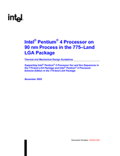
Intel Pentium 4 Datasheet (81 pages)
Pentium 4 Processor on 90 nm Process
Brand:
Intel
| Category:
Computer Hardware
| Size: 1.89 MB
Table of Contents
Table of Contents
3
Revision History
7
Introduction
9
Terminology
10
Processor Packaging Terminology
10
References
11
Electrical Specifications
13
Power and Ground Pins
13
Decoupling Guidelines
13
VCC Decoupling
13
FSB GTL+ Decoupling
13
FSB Clock (BCLK[1:0]) and Processor Clocking
14
Voltage Identification
14
Core Frequency to FSB Multiplier Configuration
14
Voltage Identification Definition
15
Phase Lock Loop (PLL) Power and Filter
16
Phase Lock Loop (PLL) Filter Requirements
16
Reserved, Unused, and TESTHI Pins
17
FSB Signal Groups
18
FSB Pin Groups
18
Asynchronous GTL+ Signals
19
Test Access Port (TAP) Connection
19
Signal Characteristics
19
Signal Reference Voltages
19
FSB Frequency Select Signals (BSEL[1:0])
20
BSEL[1:0] Frequency Table for BCLK[1:0]
20
Absolute Maximum and Minimum Ratings
21
Processor DC Specifications
21
Processor DC Absolute Maximum Ratings
21
Voltage and Current Specifications
22
VCC Static and Transient Tolerance for Loadline a
23
VCC Static and Transient Tolerance for Loadline a
24
VCC Static and Transient Tolerance for Loadline B
26
GTL+ Signal Group DC Specifications
27
Asynchronous GTL+ Signal Group DC Specifications
27
PWRGOOD and TAP Signal Group DC Specifications
28
VCCVID DC Specifications
28
VIDPWRGD DC Specifications
28
VCC
29
CC Overshoot Specification
29
BSEL [1:0] and VID[5:0] DC Specifications
29
BOOTSELECT DC Specifications
29
VCC Overshoot Specifications
29
Die Voltage Validation
30
Package Mechanical Specifications
31
Processor Package Assembly
31
Package Mechanical Drawing
32
Processor Package Drawing (Sheet 1 of 2)
33
Processor Package Drawing (Sheet 2 of 2)
34
Processor Component Keep-Out Zones
35
Package Loading Specifications
35
Package Handling Guidelines
35
Processor Loading Specifications
35
Package Insertion Specifications
36
Processor Mass Specification
36
Processor Materials
36
Processor Markings
36
Processor Top-Side Markings
36
Processor Pinout Coordinates
37
Processor Pinout Coordinates (Top View)
37
Pin List and Signal Description
39
Processor Pin Assignments
39
Pinout Diagram (Top View-Left Side)
40
Pinout Diagram (Top View-Right Side)
41
Alphabetical Pin Assignment
42
Numerical Pin Assignment
48
Alphabetical Signals Reference
54
Signal Description
54
Thermal Specifications and Design Considerations
63
Processor Thermal Specifications
63
Thermal Specifications
63
Processor Thermal Specifications
64
Thermal Profile
65
Thermal Metrology
66
Thermal Profile
66
Processor Thermal Features
67
Thermal Monitor
67
On-Demand Mode
68
PROCHOT# Signal Pin
68
THERMTRIP# Signal Pin
69
T Control and Fan Speed Reduction
69
Thermal Diode
69
Thermal Diode Parameters
70
Thermal Diode Interface
70
Features
71
Power-On Configuration Options
71
Power-On Configuration Option Pins
71
Clock Control and Low Power States
72
Normal State-State 1
72
Autohalt Powerdown State-State 2
72
Stop Clock State Machine
72
Stop-Grant State-State 3
73
Halt/Grant Snoop State-State 4
73
Sleep State-State 5
74
Boxed Processor Specifications
75
Mechanical Representation of the Boxed Processor
75
Mechanical Specifications
76
Boxed Processor Cooling Solution Dimensions
76
Space Requirements for the Boxed Processor (Side View)
76
Boxed Processor Fan Heatsink Weight
77
Space Requirements for the Boxed Processor (Top View)
77
Boxed Processor Retention Mechanism and Heatsink Attach Clip Assembly
78
Electrical Requirements
78
Fan Heatsink Power Supply
78
Boxed Processor Fan Heatsink Power Cable Connector Description
78
Thermal Specifications
79
Boxed Processor Cooling Requirements
79
Baseboard Power Header Placement Relative to Processor Socket
79
Fan Heatsink Power and Signal Specifications
79
Boxed Processor Fan Heatsink Airspace Keep-Out Requirements (Side 1 View)
80
Boxed Processor Fan Heatsink Airspace Keep-Out Requirements (Side 2 View)
80
Variable Speed Fan
81
Boxed Processor Fan Heatsink Set Points
81
Advertisement
Intel Pentium 4 Specification (75 pages)
Processor on 90 nm Process
Brand:
Intel
| Category:
Computer Hardware
| Size: 0.65 MB
Table of Contents
Table of Contents
3
Revision History
4
Preface
6
Summary Tables of Changes
8
General Information
21
Identification Information
23
Errata
30
Specification Changes
73
Specification Clarifications
74
Documentation Changes
75
Intel Pentium 4 Specification (74 pages)
Specification Update
Brand:
Intel
| Category:
Computer Hardware
| Size: 0.49 MB
Table of Contents
Table of Contents
3
Revision History
4
Preface
9
Summary Tables of Changes
11
General Information
21
Identification Information
24
Errata
31
System Memory
35
Specification Changes
69
Specification Clarifications
70
Documentation Changes
74
INTEL Pentium 4 Design Manual (15 pages)
Processor in 478-pin package 845 chipset platform for SDR
Brand:
INTEL
| Category:
Computer Hardware
| Size: 1.15 MB
Table of Contents
Table of Contents
3
Revision History
4
Preface
5
Nomenclature
5
Codes Used in Summary Table
6
General Design Considerations
7
Schematic, Layout, and Routing Updates
9
Documentation Changes
11
Signal Description
15
Intel Pentium 4 Design Manual (9 pages)
Brand:
Intel
| Category:
Computer Hardware
| Size: 0.12 MB
Table of Contents
Intel Pentium 4 Processor
1
Table of Contents
3
1 Overview
4
Related Documents
4
Table 1. Related Documents
4
2 Thermal-Mechanical Support Solution
5
Figure 1. Direct Chassis-Attach Example
5
Table 2. Design Summary
6
Figure 2. ATX Motherboard Hole Locations for Direct Chassis-Attach
7
Motherboard Design
7
Chassis Design
8
Figure 3. ATX Chassis Mounting Holes for Pentium® 4 Processors
8
Hardware
9
3 Conclusion
9
Intel Pentium 4 Installation Notes (11 pages)
Brand:
Intel
| Category:
Computer Hardware
| Size: 1.79 MB
Intel Pentium 4 Installation Notes (2 pages)
Brand:
Intel
| Category:
Processor
| Size: 0.14 MB
Table of Contents
Before Installing the Processor
1
Installing the Processor
1
Installing the Heatsink
2
Consulting Motherboard Documentation
2
Intel Pentium 4 Installation Notes (2 pages)
Brand:
Intel
| Category:
Computer Hardware
| Size: 0.27 MB
Intel Pentium 4 Product Overview (2 pages)
Processors with Hyper-Threading Technology for Embedded Computing
Brand:
Intel
| Category:
Computer Hardware
| Size: 0.15 MB
Advertisement
Related Products
Intel 460GX
Intel 440GX
Intel Pentium 4 mPGA478
Intel SL8K2 - Pentium 4 3.20EGHz 800MHz 1MB Socket 478 CPU
Intel UPI- 41A
Intel UPI- 41AH
Intel UPI- 42AH
Intel Pentium 4 570
Intel Pentium 4 571
Intel Pentium 4 560
Intel Categories
Motherboard
Computer Hardware
Server
Server Board
Desktop
More Intel Manuals
Login
Sign In
OR
Sign in with Facebook
Sign in with Google
Upload manual
Upload from disk
Upload from URL