Table of Contents
Advertisement
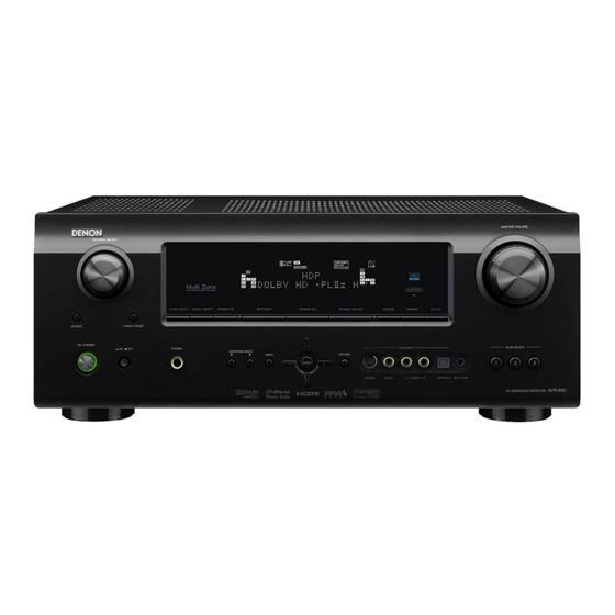
MODEL
AVR-2310CI
AVR-2310
AVR-890
MODEL
AVC-2310
For purposes of improvement, specifications and design are subject to change without notice.
●
Please use this service manual with referring to the operating instructions without fail.
●
Some illustrations using in this service manual are slightly different from the actual set.
●
X0415V03DM/DG0910
SERVICE MANUAL
JP
AV SURROUND RECEIVER
JP
AV SURROUND AMPLIFIER
e
D&M Holdings lnc.
Copyright 2009 D&M Holdings Inc. All rights reserved.
WARNING: Violators will be prosecuted to the maximum extent possible.
E3
E2
EK
E3
E2
EK
Ver. 3
Please refer to the
MODIFICATION NOTICE.
EA
E1C E1K EUT
EA
E1C E1K EUT
Advertisement
Table of Contents

Related Manuals for Denon AVR-2310


Summary of Contents for Denon AVR-2310
- Page 1 Ver. 3 Please refer to the MODIFICATION NOTICE. SERVICE MANUAL MODEL E1C E1K EUT AVR-2310CI AVR-2310 AVR-890 AV SURROUND RECEIVER MODEL E1C E1K EUT AVC-2310 AV SURROUND AMPLIFIER For purposes of improvement, specifications and design are subject to change without notice.
-
Page 2: Safety Precautions
SAFETY PRECAUTIONS The following check should be performed for the continued protection of the customer and service technician. LEAKAGE CURRENT CHECK Before returning the unit to the customer, make sure you make either (1) a leakage current check or (2) a line to chassis resistance check. -
Page 3: Dimensions
DIMENSION AVR-2310CI/2310, AVC-2310 model AVR-2310CI/2310/890, AVC-2310... - Page 4 AVR-890 model AVR-2310CI/2310/890, AVC-2310...
- Page 5 WIRE ARRANGEMENT If wire bundles are untied or moved to perform adjustment or parts replacement etc., be sure to rearrange them neatly as they were originally bundled or placed afterward. Otherwise, incorrect arrangement can be a cause of noise generation. Wire arrangement viewed from the top Back Panel side Front Panel side...
-
Page 6: Disassembly
DISASSEMBLY • Disassemble in order of the arrow of the figure of following flow. • In the case of the re-assembling, assemble it in order of the reverse of the following flow. • In the case of the re-assembling, observe "attention of assembling" it. CABINET TOP PANEL FRONT ASSY PCB HDMI ASSY... - Page 7 About the photos used for descriptions in the “DISASSEMBLY” section. • The direction from which the photographs used herein were photographed is indicated at "Direction of photograph: ***" at the left of the respective photographs. • Refer to the table below for a description of the direction in which the photos were taken. •...
- Page 8 (3) Loose the Cord holders, then disconnect the connector wires. Cord holder : Loose CN305 CN303 CN306A Cord holder : Loose CP503 (4) Disconnect the FFC Cable. Direction of photograph: C FFC Cable (5) Remove the screws. (6) Disconnect the connector wire, then remove the screw. CP541 Direction of photograph: D Please refer to "EXPLODED VIEW"...
- Page 9 2. PCB HDMI ASSY → Proceeding : CABINET TOP HDMI PWB ASSY (1) Cut the wire clamp band, then disconnect the connector wires and FFC Cables. Remove the SUPPORTER, then disconnect the board to board. FFC Cable CX046 FFC Cable CX047 SUPPORTER FFC Cable...
- Page 10 4. PCB DIGI-CNT ASSY → → Proceeding : CABINET TOP HDMI PWB ASSY BRACKET HDMI → DIGI-CNT PWB ASSY (1) Disconnect the FFC cable and board to board. Board to board FFC Cable PCB DIGI-CNT ASSY (2) Remove the screws. Direction of photograph: A 5.
- Page 11 6. CHASSIS BACK → → Proceeding : CABINET TOP HDMI PWB ASSY BRACKET HDMI → DIGI-CNT PWB ASSY → TUNER PACK → CHASSIS BACK (1) Cut the wire clamp band, then loose the style pins. Disconnect the connector wires. Style pin : Loose CP102B CN102 CN101B...
- Page 12 7. PCB SIRIUS ASSY → → Proceeding : CABINET TOP HDMI PWB ASSY BRACKET HDMI → DIGI-CNT PWB ASSY → TUNER PACK → CHASSIS BACK → PCB SIRIUS ASSY (1) Disconnect the board to board. Board to board PCB DSIRIUS ASSY 8.
- Page 13 9. PCB INPUT ASSY → → Proceeding : CABINET TOP HDMI PWB ASSY BRACKET HDMI → DIGI-CNT PWB ASSY → TUNER PACK → CHASSIS BACK → PCB SIRIUS ASSY → PCB VIDEO ASSY → PCB INPUT ASSY (1) Cut the wire clamp bands. Direction of photograph: C (2) Loose the Cord holder, then disconnect the connector wires and board to board.
- Page 14 10. PCB CPU ASSY → → Proceeding : CABINET TOP HDMI PWB ASSY BRACKET HDMI → DIGI-CNT PWB ASSY → TUNER PACK → CHASSIS BACK → PCB SIRIUS ASSY → PCB VIDEO ASSY → PCB INPUT ASSY → PCB CPU ASSY (1) Disconnect the FFC cable.
- Page 15 11. PCB MAIN ASSY → → Proceeding : CABINET TOP HDMI PWB ASSY BRACKET HDMI → DIGI-CNT PWB ASSY → TUNER PACK → CHASSIS BACK → PCB SIRIUS ASSY → PCB VIDEO ASSY → PCB INPUT ASSY → PCB CPU ASSY →...
- Page 16 12. PCB SUPPLY and PCB POWER → → Proceeding : CABINET TOP HDMI PWB ASSY BRACKET HDMI → DIGI-CNT PWB ASSY → TUNER PACK → CHASSIS BACK → PCB SUPPLY and PCB POWER (1) Disconnect the connector wires, then remove the screws. CP515 CP501 PCB SUPPLY ASSY...
- Page 17 13. TRANS MAIN → Proceeding : CABINET TOP TRANS MAIN (1) Cut the wire clamp bands, then disconnect the connector wires and SUPPORTER. CP513 CP512 Direction of photograph: D CP301 (2) Cut the wire clamp band, then loose the style pin. Disconnect the connector wires, then remove the screws. CP2270 CN306A Style pin : Loose...
- Page 18 14. PCB PRE OUT ASSY (E2/EA/E1C model) → → Proceeding : CABINET TOP HDMI PWB ASSY BRACKET HDMI → DIGI-CNT PWB ASSY → TUNER PACK → PCB PRE OUT ASSY (1) Disconnect the connector wires. CN701 CN702 PCB PRE-OUT ASSY (2) Remove the screws.
-
Page 19: Initializing Av Surround Receiver
MODE 1 JIG to use for servicing When you repair the printing board, you can use the following JIG (Extension cable kit). Please order to Denon Official Service Distributor in your region if necessary. 00D SPK- 561 EXTENSION UNIT KIT : 1 Set 00D SPK- 562 9120 CONN. -
Page 20: Special Mode Setting Button
SPECIAL MODE d Special mode setting button ※ Press the ON/OFF button to turn on while pressing both buttons A and B at the same time. Mode Button A Button B Contents Serial No. and firmware versions such as Main, Sub, DSP are µcom/DSP Version display mode STATUS DIMMER... -
Page 21: Μcom/Dsp Version Display Mode
1. µcom/DSP Version display mode 1.1. Operation specifications µcom/DSP version display mode: When started up, the version information is displayed. Starting up: With the "DIMMER" and "STATUS" buttons pressed, press the "ON/OFF" button to turn the power on. Now, press the "STATUS" button to the display the 2nd item information on the FL Display. 1.2. - Page 22 2. Errors checking mode (Displaying the protection history) 2.1. Operation specifications Error mode (Displaying the protection history): When started up, the error information is displayed. Starting up: ● All model commonness With the "STATUS" and "MULTEQ" buttons pressed, press the "ON/OFF" button to turn the power on. The error (protection history display) mode is set.
-
Page 23: Audio Section
ADJUSTMENT Audio Section Idling Current Required measurement equipment: DC Voltmeter 1. Preparation (1) Avoid direct blow from an air conditioner or an electric fan, and adjust the unit at normal room temperature 15 °C ~ 30 °C (59 °F ~ 86 °F). (2) Presetting •... -
Page 24: Trouble Shooting
TROUBLE SHOOTING 1. POWER 1.1. Power not turn on Power not turn on Are there any incomplete Is the ON/STANDBY indica- there short circuit Correct the short circuit connections in the connec- tor on the front panel flashing between the speaker termi- between the speaker and tors connecting between the red? -
Page 25: Analog Video
2. Analog video 2.1. MONITOR OUT MONITOR OUT (CVBS/S/COMPONENT) output NG ※ When checking operation, select SAT/CBL for the function of CVBS/ S, and select DVD for the function of COMPONENT. Check the Video convert ON/OFF settings (COMPONENT1 input) Video convert ON Input Input Input... - Page 26 Input CVBS/S Check Power Supply Voltages. V+5 : CN2005-8pin OSD3.3V : TP602-2pin V-5 : CN2005-7pin I/P_3.3V : FB851 To troubleshooting SCPU+5V : CY141-1pin DDR_1.8V : CC805 (L802 side) 1.1 Power not turn on. CEC3.3V : C420 (IC402 side) 1.0V_DV : CC809 (L801 side) CEC1.8V : C428 (IC403 side) Check input selector and Video AMP, PCB HDMI...
- Page 27 Input COMPONENT Check Power Supply Voltages. V+5 : CN2005-8pin OSD3.3V : TP602-2pin V-5 : CN2005-7pin I/P_3.3V : FB851 To troubleshooting SCPU+5V : CY141-1pin DDR_1.8V : CC805 (L802 side) 1.1 Power not turn on. CEC3.3V : C420 (IC402 side) 1.0V_DV : CC809 (L801 side) CEC1.8V : C428 (IC403 side) Check input selector and Video AMP, PCB HDMI...
- Page 28 2.2. HDMI OUT HDMI OUT output NG ※ When checking operation, select SAT/CBL for the function of CVBS/ S, and select DVD for the function of COMPONENT. (COMPONENT1 input) Check the Video convert ON/OFF settings Video convert ON Input Input Input Input CVBS...
- Page 29 Input CVBS/S Check Power Supply Voltages. V+5 : CN2005-8pin OSD3.3V : TP602-2pin V-5 : CN2005-7pin I/P_3.3V : FB851 To troubleshooting SCPU+5V : CY141-1pin DDR_1.8V : CC805 (L802 side) 1.1 Power not turn on. CEC3.3V : C420 (IC402 side) 1.0V_DV : CC809 (L801 side) CEC1.8V : C428 (IC403 side) Check input selector and Video AMP, PCB HDMI...
- Page 30 2.3. VCR/DVR MONITOR OUT VCR/DVR MONITOR OUT(CVBS/S) output NG ※ When checking operation, select SAT/CBL for the function. Input Input Input CVBS COMPONENT No output Input CVBS/S Check signal V ± 5, SCPU+5V. To troubleshooting V+5 : CN2005-8pin 1.1 Power not turn on. V-5 : CN2005-7pin SCPU+5V : CY141-1pin Check input selector and Video AMP,...
- Page 31 Is the DVD player's HDMI referring to the DVD player's output setting correct? operating instructions. When using a DENON DVD player, is the fluorescent display tube's "HDMI" indicator lit? If using a non-DENON DVD player, proceed to "YES". Are the picture and sound...
- Page 32 VIDEO out or Component out)? surrounding circuitry) The DVD player does not recognize connection with the set. When using a DENON DVD Is the HDMI connector (JK502/ The pattern and circuit from player, fluorescent JK503/JK401/JK402/JK403) the HDMI connector (JK502/ display tube's "HDMI" indicator pin 19 "H"...
- Page 33 BLOCK DIAGRAM AUDIO BLOCK DIAGRAM AVR-2310CI/2310/890, AVC-2310...
-
Page 34: Video Block Diagram
VIDEO BLOCK DIAGRAM AVR-2310CI/2310/890, AVC-2310... - Page 35 VCC DIAGRAM S1(AMP +B) S2(+12V,-12V) AC OUTLET S3(DSP.HDMI) MAIN TRANS AC CORD S4(VIDEO) S5(VH) S6(FILAMENT) SUB TRANS AVR-2310CI/2310/890, AVC-2310...
- Page 36 LEVEL DIAGRAMS FRONT LEVEL DIAGRAM LEVEL DIAGRAM FRONT ch AVR-2310CI/2310/890, AVC-2310...
- Page 37 CENTER LEVEL DIAGRAM LEVEL DIAGRAM CENTER ch AVR-2310CI/2310/890, AVC-2310...
- Page 38 SUB WOOFER LEVEL DIAGRAM LEVEL DIAGRAM SUBWOOFER ch AVR-2310CI/2310/890, AVC-2310...
- Page 39 SURROUND LEVEL DIAGRAM LEVEL DIAGRAM SURROUND ch AVR-2310CI/2310/890, AVC-2310...
- Page 40 SURROUND BACK LEVEL DIAGRAM LEVEL DIAGRAM SURR.BACK ch AVR-2310CI/2310/890, AVC-2310...
- Page 41 CLOCK FLOW & WAVE FORM IN DIGITAL BLOCK Wave form CH1: D-DATA ② ① CH1: DATA CH2: fs CH3: 64fs CH1: DATA CH2: fs CH3: 64fs CH4: 256fs ③ AVR-2310CI/2310/890, AVC-2310...
- Page 42 ---MEMO--- AVR-2310CI/2310/890, AVC-2310...
- Page 43 SEMICONDUCTORS Only major semiconductors are shown, general semiconductors etc. are omitted to list. The semiconductor which described a detailed drawing in a schematic diagram are omitted to list. 1. IC’s M30879FLBFP (IC802 : CPU B’D) ( note 6) ( note 6) D7 / AN0_7 / P0_7 P4_4 / CS3 / A20 <VCC2>...
- Page 44 M30879FLBFP Block Diagram Port P0 Port P1 Port P2 Port P3 Port P4 Port P5 Port P6 Port P7 <VCC2> <VCC1> Internal peripheral functions Timers (16 bits) Clock generation circuits: 10-bit A/D converter: Output (timer A): 5 XIN-XOUT 1 circuit Input (timer B): 6 XCIN-XCOUT 34 channels for input...
- Page 45 PURE STBY P.OFF PIN NAME I/O Type DET Function (in) (ex) STBY STOP STOP 17 P85/NMI 18 P84/INT2 PROTECTION Fall Edge & L PROTECTION Detect E ↓&L 19 P83/INT1 POWERKEY POWER key operation det 20 P82/INT0 D.OSD CPU REQ Interface between Main CPU and D.OSD CPU 21 P81 D.OSD CPU ACK...
- Page 46 PURE STBY P.OFF PIN NAME I/O Type DET Function (in) (ex) STBY STOP STOP 66 P26 SCPUPOWER H:SCPU Sub CPU power control POWER ON 67 P25 SIRIUS RESET SIRIUS control 68 P24 POWER H:POWER ON Main power relay control 69 P23 70 P22 LIMIT H : ON...
- Page 47 R5F3650TNFB (IC901 : HDMI B’D) P1_2/RXD6/SCL6/D10 P4_2/A18 P1_1/CLK6/D9 P4_3/A19 VCC2 ports P1_0/CTS6/RTS6/D8 P4_4/CTS7/RTS7/CS0 P0_7/AN0_7/D7 P4_5/CLK7/CS1 P0_6/AN0_6/D6 P4_6/PWM0/RXD7/SCL7/CS2 P0_5/AN0_5/D5 P4_7/PWM1/TXD7/SDA7/CS3 P0_4/AN0_4/D4 P5_0/WRL/WR M16C/65 Group P0_3/AN0_3/D3 P5_1/WRH/BHE P0_2/AN0_2/D2 P5_2/RD P0_1/AN0_1/D1 P5_3/BCLK P0_0/AN0_0/D0 P5_4/HLDA P10_7/AN7/KI3 P5_5/HOLD PLQP0100KB-A P10_6/AN6/KI2 P5_6/ALE P10_5/AN5/KI1 P5_7/RDY/CLKOUT (100P6Q-A) P10_4/AN4/KI0 P6_0/RTCOUT/CTS0/RTS0 P10_3/AN3 P6_1/CLK0...
- Page 48 R5F3650TNFB Block Diagram Port P0 Port P2 Port P3 Port P4 Port P5 VCC1 ports Internal peripheral functions System clock generator UART or clock synchronous serial I/O XIN-XOUT Timer (16-bit) (3 channels) XCIN-XCOUT PLL frequency synthesizer UART Outputs (timer A) : 5 On-chip oscillator (125 kHz) (1 channel) Inputs (timer B) : 6...
- Page 49 PURE P.OF PIN NAME I/O Type Op(ex) Res CEC STBY Function (in) 21 P77/(CLK5) SI CODECO CODEC(ADAU1328) control 22 P76/(TXD5) TMS/M/D O/L FPGA firmware update control (JTAG) 23 P75 FPGA firmware update control (JTAG) 24 P74 MTCK FPGA firmware update control (JTAG) 25 P73/(CTS2) ANALOG VIDEO Analog video components power control...
- Page 50 PURE P.OF PIN NAME I/O Type Op(ex) Res CEC STBY Function (in) 76 P12/RXD6 DSP MISO DSP (ADSP-21367-333) control 77 P11/CLK6 DSPICLK DSP (ADSP-21367-333) control 78 P10 Z1VSIG.DET Video signal (CVBS) detect 79 P07 PLD WRITE PLD(EPM240T100C5N) firmware update control 80 P06 VPLD CE MODE1=O/H...
- Page 51 ADSP-21367 (IC254 : HDMI B’D) PIN 1 INDICATOR TOP VIEW (PINS DOWN) ADSP-21367 Terminal Function Pin No. Signal Pin No. Signal Pin No. Signal Pin No. Signal DATA28 DATA27 IOVDD IOVDD ADDR0 SDCAS IOVDD ADDR2 SDRAS DATA26 ADDR1 SDCKE DATA25 ADDR4 SDWE DATA24...
- Page 52 ADV7510 (IC701 : HDMI B’D) PIN 1 VSYNC INDICATOR DSD0 DSD1 DSD2 DSD3 DSD4 DSD5 DSD_CLK SPDIF MCLK ADV7510 I2S0 TOP VIEW (Not to Scale) I2S1 I2S2 I2S3 SCLK LRCLK DDCSDA DDCSCL ADV7510 Block Diagram CEC Controller/ Buffer S/PDIF S/PDIF S[3:0] S[3:0] HDCP...
- Page 53 IS42S32200E-6TL (IC603 : HDMI B’D) IS42S32200E-6TL Block Diagram AVR-2310CI/2310/890, AVC-2310...
- Page 54 IS42S32200E-6TL Terminl Function AVR-2310CI/2310/890, AVC-2310...
- Page 55 R2A15218FP (IC700 : INPUT B’D) R2A15218FP Block Diagram 50 49 48 47 46 45 44 43 42 41 40 39 38 37 36 35 34 33 32 31 MUTE AVCC AVCC N.C. AVEE AVEE N.C. TREL 0/-6/-12/-18dB ADCL BASSL2 ADCR BASSL1 N.C.
- Page 56 R2A15218FP Terminl Function PIN No. Function Name 23,21, FROUT,FLO UT, 17,15, COUT,SWOUT, Output pin of FL/ FR/C/SW/SL/ SR/SBL/ SBR channel 11,9, SROUT, SLO UT, SBROUT,S BL OUT 24,20, FRC,FLC, 18,14, CC,SWC, Connects capacitor fo r reducing click no ise of 12,8, SRC,SLC, L/R /C/SW/SL/SR/SBL/ SBR channel vol ume...
- Page 57 ADV3002XSTZ (IC401 : HDMI B’D) ADV3002XSTZ Block Diagram AVR-2310CI/2310/890, AVC-2310...
- Page 58 ADV3002XSTZ Pin Description AVR-2310CI/2310/890, AVC-2310...
- Page 59 AVR-2310CI/2310/890, AVC-2310...
- Page 60 W9864G2GH-6 (IC253 : HDMI B’D) W9864G2GH-6 Block Diagram AVR-2310CI/2310/890, AVC-2310...
- Page 61 W9864G2GH-6 Pin Description AVR-2310CI/2310/890, AVC-2310...
- Page 62 ADV7340BSTZ (IC952 : HDMI B’D) ADV7340BSTZ Block Diagram AVR-2310CI/2310/890, AVC-2310...
- Page 63 ADV7340BSTZ Pin Description AVR-2310CI/2310/890, AVC-2310...
- Page 64 LC89058W-E (IC101 : HDMI B’D) 35 34 33 32 31 30 29 28 27 26 25 SDIN SLRCK SBCK RDATA RLRCK XMODE DGND DV DD LC89058W-E DV DD DGND GPIO0 RBCK GPIO1 RMCK AGND GPIO2 AV DD GPIO3 RXOUT2 * : Pull-down resistor internal at no selection Pin Functions RXOUT1 RX0-6 input S/PDIF through output pin 1...
- Page 65 Pin No. Name Function DGND Digital GND DV DD Digital power supply (3.3V) XMCK Oscillation amplifier clock output pin XOUT Output pin connected to the resonator External clock input pin, connected to the resonator (12.288MHz/24.576MHz) DV DD Digital power supply DGND Digital GND MOUT...
- Page 66 ADAU1328 (IC301 : HDMI B’D) AVR-2310CI/2310/890, AVC-2310...
- Page 67 EN29LV160BB-70TIP (IC255 : HDMI B’D) BYTE# DQ15/A-1 DQ14 DQ13 Standa rd DQ12 TSOP RESET# DQ11 RY/BY# DQ10 EN29LV160BB-70TIP Block Diagram RY/BY# DQ0-DQ15 (A-1) Block Protect Switches Erase V oltageGenerato r Input/Output Buffers State Control Program Voltage Generato r Command Chip Enable Regi s ter Data Latch Output Enable...
- Page 68 NJW1321FP1 (IC2023 : VIDEO B’D) Block Diagram AVR-2310CI/2310/890, AVC-2310...
- Page 69 LA73062V-TLM-E (IC2024 : VIDEO B’D) CV_OUT 1000 F MUTE 6MHz Driver Y_IN 0.1 F 6MHz CLAMP _DR_SD Y_OUT 1000 F MUTE SW1:SD Mute CTL Driver C_IN 0.1 F BIAS 6MHz GND_DR_SD 100k C_OUT MUTE GND_SD Driver REG3V S_DET_IN S_DET_OUT (High/Open/Low) 47 F VREG_3V SW2:Power...
- Page 70 LA73053 (IC2016 : VIDEO B’D) AVR-2310CI/2310/890, AVC-2310...
- Page 71 LC72722PM-TLM-E (IC801 : CPU B’D : E2 model) V REF MPXIN Vdda Vssa FLOUT LC72722 RDS-ID LC72722M SYNC LC72722PM T7(CORREC/ARI-ID/TA/BEO) T3(RDCL) T6(ERROR/57K/TP/BE1) T4(RDDA) Vssd T5(RSFT) Vddd X OUT X IN Top view Block Diagram V REF FLOUT Vdda Vddd CLOCK RECOVERY REFERENCE (57 kHz)
- Page 72 EN5311Q (IC202, 805 : HDMI B’D) ground. One or more of these pins may be connected internally. (Pin 15): Sense pin for output voltage SENSE regulation. Connect V to the output SENSE voltage rail as close to the terminal of the output filter capacitor as possible.
- Page 73 EN5335QI-T (IC402 : HDMI B’D) EN5335QI-T Block Diagram PVIN power UVLO Good Logic Thermal Limit ROCP Current Limit Over Voltage Over Voltage P-Drive N-Drive Comp PGND Compensation Network Sawtooth VSENSE Generator Voltage Selector Error ENABLE Reference Soft Start Voltage selector Bandgap Reference COMP...
- Page 74 EN5335QI-T Pin descriptions NAME FUNCTION NO CONNECT – Do not electrically connect these pins to each other or to PCB. CAUTION!: May be internally connected. Regulated converter output. Connect these pins to the load and place output 8-14 VOUT capacitor from these pins the PGND pins 17-18 NO CONNECT –...
- Page 75 EN5322QI-T (IC155, 403 : HDMI B’D) EN5322QI-T Block Diagram PVIN UVLO Thermal Limit Current Limit NC (SW) ENABLE Soft Start P-Drive Logic VOUT Comp N-Drive PGND VSENSE Sawtooth Generator Compensation Network Switch Error Voltage VREF BIAS Select Package Boundary AVIN AGND VS0 VS1 VS2 AVR-2310CI/2310/890, AVC-2310...
- Page 76 EN5322QI-T Pin descriptions NAME FUNCTION No Connect. These pins are internally connected to the common drain output of the internal MOSFETs. NC(SW) pins are not to be electrically connected to any external signal, ground, or 1, 21-24 NC(SW) voltage. However, they must be soldered to the PCB. Failure to follow this guideline may result in part malfunction or damage.
- Page 77 2. FL DISPLAY FLT (19-ST-03GINK) (FLT301) PIN CONNECTION GRID ASSIGNMENT AVR-2310CI/2310/890, AVC-2310...
- Page 78 ANODE CONNECTION AVR-2310CI/2310/890, AVC-2310...
- Page 79 PRINTED WIRING BOARDS PCB MAIN ASS’Y (1/2) COMPONENT SIDE AVR-2310CI/2310/890, AVC-2310...
- Page 80 PCB MAIN ASS’Y (2/2) FOIL SIDE AVR-2310CI/2310/890, AVC-2310...
- Page 81 PCB POWER ASS’Y (1/2) COMPONENT SIDE AVR-2310CI/2310/890, AVC-2310...
- Page 82 PCB POWER ASS’Y (2/2) FOIL SIDE AVR-2310CI/2310/890, AVC-2310...
- Page 83 PCB FRONT ASS'Y (1/2) COMPONENT SIDE AVR-2310CI/2310/890, AVC-2310...
- Page 84 PCB FRONT ASS'Y (2/2) FOIL SIDE AVR-2310CI/2310/890, AVC-2310...
- Page 85 PCB 2CH ASS’Y COMPONENT SIDE FOIL SIDE AVR-2310CI/2310/890, AVC-2310...
- Page 86 PCB INPUT ASS’Y COMPONENT SIDE FOIL SIDE AVR-2310CI/2310/890, AVC-2310...
- Page 87 PCB DIGI CNT ASS’Y FOIL SIDE COMPONENT SIDE AVR-2310CI/2310/890, AVC-2310...
- Page 88 PCB VIDEO ASS’Y (1/2) COMPONENT SIDE AVR-2310CI/2310/890, AVC-2310...
- Page 89 PCB VIDEO ASS’Y (2/2) FOIL SIDE AVR-2310CI/2310/890, AVC-2310...
- Page 90 PCB CPU ASS’Y FOIL SIDE COMPONENT SIDE AVR-2310CI/2310/890, AVC-2310...
- Page 91 PCB HDMI ASS’Y (1/2) COMPONENT SIDE AVR-2310CI/2310/890, AVC-2310...
- Page 92 PCB HDMI ASS’Y (2/2) FOIL SIDE AVR-2310CI/2310/890, AVC-2310...
- Page 93 PCB SPK ASS’Y PCB PRE OUT ASSY COMPONENT SIDE COMPONENT SIDE FOIL SIDE FOIL SIDE AVR-2310CI/2310/890, AVC-2310...
- Page 94 PCB SIRIUS ASS’Y PCB DIGI POWER ASSY PCB REG ASSY COMPONENT SIDE COMPONENT SIDE COMPONENT SIDE FOIL SIDE FOIL SIDE FOIL SIDE AVR-2310CI/2310/890, AVC-2310...
- Page 95 NOTE FOR PARTS LIST Parts for which "nsp" is indicated on this table cannot be supplied. When ordering of part, clearly indicate "1" and "I" (i) to avoid mis-supplying. Ordering part without stating its part number can not be supplied. Part indicated with the mark "★"...
- Page 96 PARTS LIST OF P.W.B. UNIT * Parts for which "nsp" is indicated on this table cannot be supplied. * The parts listed below are for maintenance only, might differ from the parts used in the unit in appearances or dimensions. Note: The symbols in the column "Remarks"...
- Page 97 Ref. No. Part No. Part Name Remarks Q'ty New Q180 00D2730471907 TR 2SC KTC3206Y J5023206Y0050S Q181-185 00D2710318909 TR 2SA 2N5401S J520254010010S Q221L 00D9630044301 TR KTC2875B(MB) J5222875B0010S Q221R 00D9630044301 TR KTC2875B(MB) J5222875B0010S Q227L 00D9630044301 TR KTC2875B(MB) J5222875B0010S Q227R 00D9630044301 TR KTC2875B(MB) J5222875B0010S Q231 00D9630121402 TR 2SA KRA104S R1...
- Page 98 Ref. No. Part No. Part Name Remarks Q'ty New RESISTORS GROUP R103 00D9639005639 R,METAL FILM 100-J,1W C060010165060S R105 00D9630232906 R,METAL FILM 47K-F,1/4W C060047343530S R106C R,METAL FILM 22-J,1W C060022065060S R106FL R,METAL FILM 22-J,1W C060022065060S R106FR R,METAL FILM 22-J,1W C060022065060S R106SL R,METAL FILM 22-J,1W C060022065060S R106SR R,METAL FILM 22-J,1W...
- Page 99 Ref. No. Part No. Part Name Remarks Q'ty New R166 R,METAL FILM 2.2K-J,1W C060022265050S R242,243 R,METAL FILM 15K-J,2W C060015366050S R246 R,METAL FILM 15K-J,2W C060015366050S R250 R,METAL FILM 15K-J,2W C060015366050S R253 R,METAL FILM 15K-J,2W C060015366050S VR101C 00D9600221109 VR,SEMI EVN-DJAA03B13 C541102115000S VR101FL 00D9600221109 VR,SEMI EVN-DJAA03B13 C541102115000S VR101FR...
- Page 100 Ref. No. Part No. Part Name Remarks Q'ty New C113SL 00D9630293709 C,ELECT 100UF-M/10V D040101082070S C113SR 00D9630293709 C,ELECT 100UF-M/10V D040101082070S C114 00D9639003097 C,FILM 0.1UF-K/250V D02010407H080S C114C 00D9630216100 C,CERAMIC 33PF-J/500V D00033006D050S C114FL 00D9630216100 C,CERAMIC 33PF-J/500V D00033006D050S C114FR 00D9630216100 C,CERAMIC 33PF-J/500V D00033006D050S C114SL 00D9630216100 C,CERAMIC 33PF-J/500V D00033006D050S C114SR...
- Page 101 Ref. No. Part No. Part Name Remarks Q'ty New OTHERS PARTS GROUP BKT101 BRACKET 0.8t/SCREW 4010210196100S CLAMP101-103 CLAMP WIRE(SOLDER) 4330000120000S CN101 CN,WIRE 10P L000161100050S CN104 CN,WIRE 8P L002131080050S CN201 CN,WIRE 7P L002131070010S CN511 CN,WIRE 9P L000600090021S CP103 CN.WAFER 3P L102526700300S CP104 CN.WAFER 3CKT L108353280360S...
- Page 102 PCB POWER ASS'Y Ref. No. Part No. Part Name Remarks Q'ty New SEMICONDUCTORS GROUP IC501 00D9600262605 IC NJM2396F05 J126239600010S IC502 00D9600195808 IC ICP-N15 J120001500030S IC511 00D2631274012 IC NJM2396F09 J126239600090S IC512 00D2630553006 IC NJM7805FA J126780500130S IC513 00D2630554005 IC NJM7905FA J126790500020S IC514 00D2630553006 IC NJM7805FA J126780500130S IC516...
- Page 103 Ref. No. Part No. Part Name Remarks Q'ty New C519 00D9630324704 C,ELECT 4700UF-M/16V D040472083200S C520 00D9630021104 C,ELECT 6800UF-M/16V D040682083000S C521-523 00D9630021900 C,FILM 0.047UF-J/100V D02047306C060S C524 00D9630293602 C,ELECT 1UF-M/50V (Pb Free) D040010087150S C525 00D9630234205 C,ELECT 10UF-M/50V D040100087070S C526,527 00D9609010133 C,ELECT 220UF-M/35V D040221085060S C528 963134004320S C,ELECT 6800UF-M/25V...
- Page 104 Ref. No. Part No. Part Name Remarks Q'ty New z SUB501 00D9630387602 POWER TRANS 120V/60HZ 2310E3 8200280150401S z SUB501 00D9630382801 POWER TRANS 230V/50HZ 2310E2 8200280150410S z SUB501 00D9630383004 POWER TRANS 220V/50,60HZ 8200280150420S CLP501 CLAMP WIRE(SOLDER) 4330000120000S CLP502 CLAMP WIRE(SOLDER) 4330000120000S CLP503 CLAMP WIRE(SOLDER) 4330000120000S...
- Page 105 PCB FRONT ASS'Y Ref. No. Part No. Part Name Remarks Q'ty New SEMICONDUCTORS GROUP IC301 963239001880S IC AZ4580M J121458000020S IC303 00D9600195808 IC ICP-N15 J120001500030S IC305 00D9630024004 IC NJM2068M J121206800020S IC365 00D9630237503 MODULE JSR1165-C E100116500040S Q302 00D9600285006 TR KRC104S J522104S00210S Q303-305 00D9600005202 TR 2SC KTC3198Y J5023198Y0000S Q312...
- Page 106 Ref. No. Part No. Part Name Remarks Q'ty New C318,319 C,CERAMIC F0.1UF-Z/50V D006104597050S C320 00D9630293602 C,ELECT 1UF-M/50V (Pb Free) D040010087150S C321 C,CERAMIC F0.1UF-Z/50V D006104597050S C322-324 C,CERAMIC 100PF-J/50V D010101167160S C325 C,CERAMIC 0.01UF-K/50V D010103777160S C326,327 C,CERAMIC 330PF-J/50V D010331167160S C328 C,CERAMIC X7R0.047UF-K/16V D011473773160S C329 00D9630234205 C,ELECT 10UF-M/50V D040100087070S...
- Page 107 Ref. No. Part No. Part Name Remarks Q'ty New CN304 CN,WIRE 3P L000500030051S CN305 CN.WAFER 4P L101200100410S CN306A CN.WAFER 5P L101100030510S CN307 CN,WIRE 10P L000700100031S CN307A CN.WAFER 5P L101100030510S CN308A CN.WAFER 7P L101100040710S CN309 CN.WAFER 11P L101200101120S CN309A CN.WAFER 7P L101100030710S CN541 CN.WAFER 3P...
- Page 108 Ref. No. Part No. Part Name Remarks Q'ty New SW307C 00D9630095305 SW,TACT SKHV10910D01 G180040500010S SW308A 00D9630095305 SW,TACT SKHV10910D01 G180040500010S SW308B 00D9630095305 SW,TACT SKHV10910D01 G180040500010S SW308C 00D9630095305 SW,TACT SKHV10910D01 G180040500010S VEC301 00D9630095305 SW,ENCODER EC16B24SO G121162400070S VEC303 00D9630095305 SW,ENCODER EC16B24SO G121162400070S FLT301 963172004670D DISPLAY,FLT 19-ST-03GINK K530190030010S HOLDER FLT...
- Page 109 PCB 2CH ASS'Y Ref. No. Part No. Part Name Remarks Q'ty New SEMICONDUCTORS GROUP Q401SBL 00D9630235301 TR 2SD2560Y J5032560Y0170S Q401SBR 00D9630235301 TR 2SD2560Y J5032560Y0170S Q402SBL 00D9630235204 TR 2SB1647Y J5011647Y0170S Q402SBR 00D9630235204 TR 2SB1647Y J5011647Y0170S Q403SBL 963219003340S TR KTC3964 J502396400010S Q403SBR 963219003340S TR 2SC KTC3964 J502396400010S Q404SBL...
- Page 110 Ref. No. Part No. Part Name Remarks Q'ty New R429SBR 00D9639006256 R,FIXED 1WJ-10 N113135610020S R440SBL 963252004160S POSISTOR 18BC471QB5RB F320184710050S R440SBR 963252004160S POSISTOR 18BC471QB5RB F320184710050S R452,453 R,METAL FILM 15K-J,2W C060015366050S VR401,402 00D9630366407 VR,SEMI CARBON EVN-DCAA03B 1KB C541102315000S CAPACITORS GROUP C402SBL 00D9630234205 C,ELECT 10UF-M/50V D040100087070S C402SBR 00D9630234205 C,ELECT 10UF-M/50V...
- Page 111 PCB INPUT ASS'Y Ref. No. Part No. Part Name Remarks Q'ty New SEMICONDUCTORS GROUP IC700 963239000650S IC R2A15218FP J084152180010S IC706,707 963239001880S IC AZ4580M J121458000020S IC715 00D9630024004 IC NJM2068M J121206800020S IC806 963239001880S IC AZ4580M J121458000020S Q700-707 00D9630044301 TR KTC2875B(MB) J5222875B0010S ZD700 00D9600222603 D,ZENER MTZJ7.5A K06007R544530S ZD702...
- Page 112 Ref. No. Part No. Part Name Remarks Q'ty New C894 C,CERAMIC 220PF-J/50V D010221167160S C894L 00D9630234205 C,ELECT 10UF-M/50V D040100087070S C894R 00D9630234205 C,ELECT 10UF-M/50V D040100087070S C895 00D9630223009 R,THICK 0-J,1/16W C20000006M160S C895L C,CERAMIC 330PF-J/50V D010331167160S C895R C,CERAMIC 330PF-J/50V D010331167160S C896 00D9630223009 R,THICK 0-J,1/16W C20000006M160S C906 C,CERAMIC 330PF-J/50V...
- Page 113 PCB VIDEO ASS'Y Ref. No. Part No. Part Name Remarks Q'ty New SEMICONDUCTORS GROUP IC2002-2004 00D2623445901 IC TC4051BFT J040405101010S IC2005,2006 232810005504S IC BD7628F-E2 J127762800010S IC2014,2015 00D2623446900 IC TC4052BFT J040405201010S IC2016 00D2623756904 IC LA73053 J127730530010S IC2019 00D9630218807 IC BU4094BCF-E2 J040140940030S IC2021,2022 00D9630327604 IC NJM2581M J127258100010S IC2023...
- Page 114 Ref. No. Part No. Part Name Remarks Q'ty New C2103 00D9630276409 C,ELECT 100UF-M/16V D040101083090S C2104 C,CERAMIC 0.01UF-K/50V D010103777160S C2105 00D9630276409 C,ELECT 100UF-M/16V D040101083090S C2106-2108 C,CERAMIC 0.1UF-K/50V D011104577160S C2109 C,CERAMIC 0.01UF-K/50V D010103777160S C2110 00D9630234205 C,ELECT 10UF-M/50V D040100087070S C2111 C,CERAMIC 0.1UF-K/50V D011104577160S C2112,2113 C,CERAMIC 0.01UF-K/50V D010103777160S...
- Page 115 Ref. No. Part No. Part Name Remarks Q'ty New CN2001 CN.WAFER 11 L101100031110S CN2005 CN.WAFER 9P L101100030910S CP2007 CN.WAFER 5P L101100040510S CY111 CN.FPC 11P L130100111110S CY121 CN.FPC 12P L130100111210S CY141 CN.FPC 14P L130100111410S CY151 CN.FPC 15P L130100111510S 963643005090S TER,RCA 1PIN G600107AY000YS 00D9630218001 TER,RCA 2PIN G60122001000YS...
- Page 116 PCB CPU ASS'Y Ref. No. Part No. Part Name Remarks Q'ty New SEMICONDUCTORS GROUP IC38 00D2622813903 SN74AHCT08PW-EL2 J040740800190S IC801 00D9630326906 IC LC72722PM-TLM-E 2310E2 J124727220010S IC802 963243005240D IC M30879FLBFP J020308790010S IC803 00D9630367307 IC SN74AHCU04PWR J040740400290S IC804 00D9630244907 IC SN74LV14APWR J040741400180S IC805 00D2622813903 IC SN74AHCT08PW-EL2 J040740800190S IC806-808...
- Page 117 Ref. No. Part No. Part Name Remarks Q'ty New C848 00D9609010010 C,ELECT 4.7UF-M/50V D0404R7087250S C849 C,CERAMIC 0.1UF-K/50V D011104577160S C850 00D9609010010 C,ELECT 4.7UF-M/50V D0404R7087250S C851 C,CERAMIC 0.1UF-K/50V D011104577160S C852 00D9609010010 C,ELECT 4.7UF-M/50V D0404R7087250S C853 C,CERAMIC 100PF-J/50V D010101167160S C854 C,CERAMIC 1000PF-K/50V D011102777160S C855 C,CERAMIC 100PF-J/50V D010101167160S...
- Page 118 PCB SIRIUS ASS'Y Ref. No. Part No. Part Name Remarks Q'ty New SEMICONDUCTORS GROUP IC901 00D9630024004 IC NJM2068M E3, EA J121206800020S IC902 00D2623174900 IC SN74HAHCT08 J040740800180S IC903 00D2623571901 IC HIN202EIBN 2310E3/E2 J040202000020S IC904 00MHC007805K0 IC TC74VHCT125AFT 2310E3/E2 J040741250080S Q906 00D9630148508 TRKTA1504S J520015040150S Q908 00D9630121606 TR KRC107S...
- Page 119 PCB PREOUT ASS'Y Ref. No. Part No. Part Name Remarks Q'ty New SEMICONDUCTORS GROUP Q137-141 00D9630120704 TR KRA102S J520010200210S Q141C 00D9630044301 TR KTC2875B(MB) J5222875B0010S Q141FL 00D9630044301 TR KTC2875B(MB) J5222875B0010S Q141FR 00D9630044301 TR KTC2875B(MB) J5222875B0010S Q141SBL 00D9630044301 TR KTC2875B(MB) J5222875B0010S Q141SBR 00D9630044301 TR KTC2875B(MB) J5222875B0010S Q141SL...
- Page 120 PCB HDMI ASS'Y Ref. No. Part No. Part Name Remarks Q'ty New SEMICONDUCTORS GROUP IC101 236810062608S IC LC89058W-E J046890580010S IC115 00D2623077900 IC TC74VHCU04FT J040740400080S IC116 00D2623412905 IC TC74VHC14FT J040741400220S IC151 963248005260D IC EPM240T100C5N J003240105010S IC153 00D2623436907 IC TC74VHC244FT J040742440030S IC155 231810037508S IC EN5322QI-T J080532200020S IC202...
- Page 121 Ref. No. Part No. Part Name Remarks Q'ty New D530,531 00D9630341305 D,ESD IMSA-6802-01A K067680200010S D533,534 00D9630341305 D,ESD IMSA-6802-01A K067680200010S D708-711 00D9630341305 D,ESD IMSA-6802-01A K067680200010S D713-720 00D9630341305 D,ESD IMSA-6802-01A K067680200010S D801-805 00D9630355401 D,SWITCHING KDS4148U K005041480030S D901 963209005300S D CHIP RSX101M-30 K125101300010S D902 963209005310S D CHIP 1SR154-400 TE25(SMD) K045154000000S...
- Page 122 Ref. No. Part No. Part Name Remarks Q'ty New C351,352 C,CERAMIC COG470PF-J/50V D010471167160S C353 C,CERAMIC COG270PF-J/50V D010271167160S C354 C,CERAMIC 0.01UF-K/50V D010103777160S C355-357 C,CERAMIC COG270PF-J/50V D010271167160S C358,359 C,CERAMIC 4.7UF-K/6.3V D011475571160S C361 00D9630325004 C,ELECT 100UF-MVG/6.3V D050101081650S C362,363 C,CERAMIC 100PF-J/50V D010101167160S C365 C,CERAMIC 100PF-J/50V D010101167160S C368,369 C,CERAMIC 10UF-K/16V...
- Page 123 Ref. No. Part No. Part Name Remarks Q'ty New C575 C,CERAMIC 0.01UF-K/50V D010103777160S C576 C,CERAMIC 0.82UF-K/10V D011824772162S C577 C,CERAMIC X7R0.039UF-K/50V D011393707160S C578-580 C,CERAMIC 0.01UF-K/50V D011103177101S C581 C,CERAMIC 0.01UF-K/50V D011103177101S C582 C,CERAMIC 0.1UF-K/16V D011104177101S C583 C,CERAMIC 10UF-K/16V D011106573200S C584-586 C,CERAMIC 0.1UF-K/16V D011104177101S C587 C,CERAMIC 10UF-K/16V...
- Page 124 Ref. No. Part No. Part Name Remarks Q'ty New C775 C,CERAMIC 0.1UF-K/16V D011104177101S C777 C,CERAMIC 10UF-K/16V D011106573200S C779 C,CERAMIC 1000PF-K/50V D011102177101S C780 C,CERAMIC 1000PF-K/50V D011102177101S C782 C,CERAMIC 0.1UF-K/16V D011104177101S C785 C,CERAMIC 0.1UF-K/16V D011104177101S C795 C,CERAMIC 1000PF-K/50V D011102177101S C797 C,CERAMIC 1000PF-K/50V D011102177101S C801 C,CERAMIC 0.1UF-K/16V...
- Page 125 Ref. No. Part No. Part Name Remarks Q'ty New C910 C,CERAMIC 1000PF-K/50V D011104177101S C911 C,CERAMIC 4.7UF-K/6.3V D011475571160S C913 C,CERAMIC 4.7UF-K/6.3V D011475571160S C915,916 C,CERAMIC 120PF-J/50V D011121167101S C917 C,CERAMIC X7R1000PF-K/50V D011102777160S C918,919 C,CERAMIC 4.7UF-K/6.3V D011475571160S C920 C,CERAMIC 1000PF-K/50V D011104177101S C922 C,CERAMIC 220PF-J/50V D011221167101S C923 C,CERAMIC 0.01UF-K/50V...
- Page 126 Ref. No. Part No. Part Name Remarks Q'ty New CC339-342 00D9630338509 C,ELECT 10UF-MVG/16V D050100083460S CC346-491 C,CERAMIC 100PF-J/50V D011101167101S CC501,502 C,CERAMIC 4.7UF-K/6.3V D011475571160S CC503 C,CERAMIC 0.01UF-K/50V D011103177101S CC504 C,CERAMIC 100PF-J/50V D011101167101S CC508 C,CERAMIC 1000PF-K/50V D011102177101S CC516,517 C,CERAMIC 1000PF-K/50V D011102177101S CC519-526 C,CERAMIC 4.7UF-K/6.3V D011475571160S CC547-549 C,CERAMIC 4.7UF-K/6.3V...
- Page 127 Ref. No. Part No. Part Name Remarks Q'ty New OTHERS PARTS GROUP JK401-403 CN.WAFER 19P L109100190070S JK502,503 CN.WAFER 19P L109100190070S JK701 CN.WAFER 19P L109100190070S L701-703 00D9630338800 COIL,CHIP FLC32C220K 22UH D307322200220S L801,802 963115005140S COIL,INDUCTOR B82464Z4103M D310824641030S L803-808 00D9630338800 COIL,CHIP FLC32C220K 22UH D307322200220S L851,852 00D9630338800 COIL,CHIP FLC32C220K 22UH...
- Page 128 Ref. No. Part No. Part Name Remarks Q'ty New TR404-407 00D9600285006 TR KRC104S J522104S00210S TR408 963219004200S CHIP FDC608PZ P-CH J543608000010S TR409 00D9630120801 TR KRC102S J522010200210S TR502,503 00D9630120801 TR KRC102S J522010200210S TR505-507 00D9600285006 TR KRC104S J522104S00210S TR601 00D9630120801 TR KRC102S J522010200210S TR602 963219004200S CHIP FDC608PZ P-CH J543608000010S...
- Page 129 PCB SPK ASS'Y Ref. No. Part No. Part Name Remarks Q'ty New SEMICONDUCTORS GROUP Q542-546 00D9630121606 TR KRC107S J522107S00210S D542-546 00D9630355401 D,SWITCHING KDS4148U K005041480030S RESISTORS GROUP R501C 00D9639006256 R,FIXED 1WJ-10 N113135610020S R501FL 00D9639006256 R,FIXED 1WJ-10 N113135610020S R501FR 00D9639006256 R,FIXED 1WJ-10 N113135610020S R501SBL 00D9639006256 R,FIXED 1WJ-10...
- Page 130 Ref. No. Part No. Part Name Remarks Q'ty New JACK501 963646001690S TER,BOARD SCREW 8P G614108V1010MS JACK503 00D9630158608 TER,BOARD SCREW 2P G611201A0200YS JACK504 963646001690S TER,BOARD SCREW 8P G614108V1010MS SPK104 963682003410S RELAY HL3-2A-12S 12V 5A G680120503020S SPK105 963682003410S RELAY HL3-2A-12S 12V 5A G680120503020S SPK106 963682003410S RELAY HL3-2A-12S 12V 5A...
- Page 131 PCB DIGI CNT ASS'Y Ref. No. Part No. Part Name Remarks Q'ty New CAPACITORS GROUP C901-915 C,CERAMIC 100PF-J/50V D010101167160S C916 963134002720S C,ELECT10UF-M/50V (Pb Free) D040100087080S OTHERS PARTS GROUP BKT801,802 BRACKET 0.8t/SCREW 4010210196100S BKT901 BRACKET 0.8t/SCREW 4010210196100S CN803 CN.WAFER 12P L101100031210S CN900 CN.WAFER 5P L101100030510S...
- Page 132 PCB DIGI POWER ASS'Y Ref. No. Part No. Part Name Remarks Q'ty New SEMICONDUCTORS GROUP IC2270,2271 963239004190S IC AOZ1021AI J048102100010S CAPACITORS GROUP C2270,2271 C,CERAMIC 10UF-K/16V D011106573200S C2272,2273 C,CERAMIC 10UF-K/25V D011106574300S C2274 C,CERAMIC X7R2200PF-K/50V D011222777200S C2275,2276 C,CERAMIC 10UF-K/16V D011106573200S C2277,2278 C,CERAMIC 10UF-K/25V D011106574300S C2281 C,CERAMIC X7R2200PF-K/50V...
- Page 133 ---MEMO--- AVR-2310CI/2310/890, AVC-2310...
- Page 134 EXPLODED VIEW WARNING: Parts marked with this symbol have critical characteristics. Use ONLY replacement parts recommended by the manufacturer. AVR-2310CI/2310/890, AVC-2310...
- Page 135 PARTS LIST OF EXPLODED VIEW * Parts for which "nsp" is indicated on this table cannot be supplied. * P.W.B. ASS'Y for which "nsp" is indicated on this table cannot be supplied. When repairing the P.W.B. ASS'Y, check the board parts table and order replacement parts. *...
- Page 136 Ref. No. Part No. Part Name Remarks Q'ty New PCB MAIN ASSY 2310CIBKE3 7025HK0818010 PCB MAIN ASSY 2310BKE2 7025HK0818050 PCB MAIN ASSY 2310SPE2 7025HK0818030 PCB MAIN ASSY 890BKE3 7025HK0818060 PCB MAIN ASSY 890BKEA 7025HK0818020 PCB MAIN ASSY 2310SPE1C 7025HK0818040 PCB INPUT ASSY 2310CIBKE3 7025HK0818014 PCB INPUT ASSY...
- Page 137 PCB REG ASSY 7020068920000S 1 963416004500D WINDOW DISPLAY 5077212762040S 2 963412000570D KNOB FUNCTION(KD) 5080211761000SZ 2 963412003660D KNOB FUNCTION 5087211901000S 3 00D9630362109 BADGE DENON 5630210028300S 3 00D9630362202 BADGE DENON 5630210028400S 4 963402004490D PANEL FRONT 2310CIBKE3 3067214351300S 4 963402004700D PANEL FRONT 2310BKE2...
- Page 138 Ref. No. Part No. Part Name Remarks Q'ty New CUSHION SIDE 4050211095000S CN WIRE L000121020230S 33 00D9630158404 AC INLET G430040560020S 34 963406004690D CHASSIS BACK 2310CIBKE3 3207212876000S 34 963406004940D CHASSIS BACK 2310BKE2/SPE2 3207212876200S 34 963406004950D CHASSIS BACK 890BKE3 3207212876100S 34 963406004960D CHASSIS BACK 890BKEA 3207212876300S 34 963406004970D CHASSIS BACK...
- Page 139 Ref. No. Part No. Part Name Remarks Q'ty New G 00D9630048307 SCREW (+2S 4*8 B-TYPE(DOT) BK/BH) 1500040083B10S G 00D9639004012 SCREW (+2S 4*8 B-TYPE(DOT) NI/BH) 1500040084B10S SCREW (+3S 4*8 P+S-WASHER ZNW/PH) B028940081B10S SCREW (+2S 3*8 ZnY WASHER PI12) 1500001456010S SCREW (+3S 4*6 S-TYPE ZNW/BH) B020740061B10S SCREW (+2S 3*5 B-TYPE ZNW/BH) B020030051B10S...
- Page 140 PACKING VIEW E3,E1C,EA model E2 model PARTS LIST OF PACKING & ACCESSORIES * Parts for which "nsp" is indicated on this table cannot be supplied. * The parts listed below are for maintenance only, might differ from the parts used in the unit in appearances or dimensions. Note: The symbols in the column "Remarks"...
- Page 141 Ref. No. Part No. Part Name Remarks Q'ty New 963541004860D INSTRUCTION MANUAL 2310SPE1C 5707000002290S 00D2310089007 AM ANTENNA WIRE E3, E2, EA E605010110010S 00D9630158006 FM ANTENNA WIRE E3, E2, EA E605010070001S 963307003600D REMOCON (RC-1117) 8300111700010S POLY BAG 6330000240000S 963533003320D CUSHION SNOW L/R 6230212514000S 963531004520D BOX GIFT...
- Page 142 NOTE FOR SCHEMATIC DIAGRAM WARNING: Parts marked with this symbol z have critical characteristics. Use ONLY replacement parts recommended by the manufacturer. CAUTION: Before returning the unit to the customer, make sure you make either (1) a leakage current check or (2) a line to chassis resistance check.
- Page 143 Analog Audio SIGNAL LINE SCHEMATIC DIAGRAMS (1/27) MAIN UNIT (1/2) AVR-2310CI/2310/890, AVC-2310...
- Page 144 SCHEMATIC DIAGRAMS (2/27) MAIN UNIT (2/2) INPUT CNT UNIT Analog Audio SIGNAL LINE AVR-2310CI/2310/890, AVC-2310...
- Page 145 Analog Audio SIGNAL LINE SCHEMATIC DIAGRAMS (3/27) SPK 1 UNIT SPK 2 UNIT SPK CNT UNIT AVR-2310CI/2310/890, AVC-2310...
- Page 146 SCHEMATIC DIAGRAMS (4/27) 2CH UNIT AVR-2310CI/2310/890, AVC-2310...
- Page 147 SCHEMATIC DIAGRAMS (5/27) Analog Audio SIGNAL LINE INPUT UNIT (1/2) AVR-2310CI/2310/890, AVC-2310...
- Page 148 Analog Audio SIGNAL LINE SCHEMATIC DIAGRAMS (6/27) INPUT UNIT (2/2) AVR-2310CI/2310/890, AVC-2310...
- Page 149 Analog Audio SIGNAL LINE SCHEMATIC DIAGRAMS (7/27) CPU UNIT (1/2) MCPU PART AVR-2310CI/2310/890, AVC-2310...
- Page 150 Digital Audio (OPT) SIGNAL LINE SCHEMATIC DIAGRAMS (8/27) CPU UNIT (2/2) DIGITAL IN PART AVR-2310CI/2310/890, AVC-2310...
- Page 151 Digital Audio (OPT) SIGNAL LINE SCHEMATIC DIAGRAMS (9/27) DIGITAL CNT UNIT AVR-2310CI/2310/890, AVC-2310...
- Page 152 SCHEMATIC DIAGRAMS (10/27) FRONT UNIT FUNCTION UNIT ENCODER CNT UNIT PWR S/W UNIT ENCODER UNIT V. AUX UNIT FUNCTION CNTUNIT H/P UNIT FUNCTION ENCODER UNIT AVR-2310CI/2310/890, AVC-2310...
- Page 153 SCHEMATIC DIAGRAMS (11/27) Video SIGNAL LINE VIDEO UNIT (1/2) S/C VIDEO PART S-Video Y-Signal SIGNAL LINE AVR-2310CI/2310/890, AVC-2310...
- Page 154 SCHEMATIC DIAGRAMS (12/27) COMPONENT Y- SIGNAL LINE VIDEO UNIT(2/3) DIGITAL UNIT Video SIGNAL LINE COMPONENT PART S-Video Y- SIGNAL LINE AVR-2310CI/2310/890, AVC-2310...
- Page 155 SCHEMATIC DIAGRAMS (13/27) SUPPLY UNIT POWER UNIT AVR-2310CI/2310/890, AVC-2310...
- Page 156 SCHEMATIC DIAGRAMS (14/27) SIRIUS UNIT RS232C UNIT AVR-2310CI/2310/890, AVC-2310...
- Page 157 Analog Audio SIGNAL LINE SCHEMATIC DIAGRAMS (15/27) PREOUT UNIT AVR-2310CI/2310/890, AVC-2310...
- Page 158 SCHEMATIC DIAGRAMS (16/27) Digital Audio (OPT) SIGNAL LINE HDMI UNIT (1/12) HDMI Audio SIGNAL LINE DIR & PLD SECTION Digital Audio SIGNAL LINE AVR-2310CI/2310/890, AVC-2310...
- Page 159 Digital Audio SIGNAL LINE SCHEMATIC DIAGRAMS (17/27) HDMI UNIT (2/12) DSP SECTION AVR-2310CI/2310/890, AVC-2310...
- Page 160 SCHEMATIC DIAGRAMS (18/27) Analog Audio SIGNAL LINE HDMI UNIT (3/12) CODEC SECTION Digital Audio SIGNAL LINE AVR-2310CI/2310/890, AVC-2310...
- Page 161 SCHEMATIC DIAGRAMS (19/27) HDMI UNIT (4/12) HDMI SW SECTION AVR-2310CI/2310/890, AVC-2310...
- Page 162 SCHEMATIC DIAGRAMS (20/27) COMPONENT Y- SIGNAL LINE HDMI UNIT (5/12) Digital Video SIGNAL LINE Video SIGNAL LINE HDMI RX SECTION HDMI/TMDS SIGNAL LINE S-Video Y- SIGNAL LINE AVR-2310CI/2310/890, AVC-2310...
- Page 163 Digital Video SIGNAL LINE SCHEMATIC DIAGRAMS (21/27) HDMI UNIT (6/12) OSD FPGA SECTION AVR-2310CI/2310/890, AVC-2310...
- Page 164 Digital Video SIGNAL LINE SCHEMATIC DIAGRAMS (22/27) HDMI/TMDS SIGNAL LINE HDMI UNIT (7/12) HDMI Audio SIGNAL LINE MIX TX SECTION AVR-2310CI/2310/890, AVC-2310...
- Page 165 COMPONENT Y- SIGNAL LINE SCHEMATIC DIAGRAMS (23/27) S-Video Y- SIGNAL LINE HDMI UNIT (8/12) V. ENCODER SECTION Digital Video SIGNAL LINE AVR-2310CI/2310/890, AVC-2310...
- Page 166 Digital Video SIGNAL LINE SCHEMATIC DIAGRAMS (24/27) HDMI UNIT (9/12) I/P SECTION AVR-2310CI/2310/890, AVC-2310...
- Page 167 SCHEMATIC DIAGRAMS (25/27) HDMI UNIT (10/12) DDR SECTION AVR-2310CI/2310/890, AVC-2310...
- Page 168 SCHEMATIC DIAGRAMS (26/27) HDMI UNIT (11/12) SUBCPU SECTION AVR-2310CI/2310/890, AVC-2310...
- Page 169 SCHEMATIC DIAGRAMS (27/27) COMPONENT Y- SIGNAL LINE Digital Audio (OPT) SIGNAL LINE HDMI UNIT (12/12) Video SIGNAL LINE Analog Audio SIGNAL LINE CONNECT SECTION S-Video Y- SIGNAL LINE AVR-2310CI/2310/890, AVC-2310...
Need help?
Do you have a question about the AVR-2310 and is the answer not in the manual?
Questions and answers