Yamaha RX-V1700 Service Manual
Av receiver/av amplifier
Hide thumbs
Also See for RX-V1700:
- Owner's manual (791 pages) ,
- Firmware update manual (3 pages) ,
- Owner's manual (151 pages)
Table of Contents
Advertisement
RX-V1700/DSP-AX1700
This manual has been provided for the use of authorized YAMAHA Retailers and their service personnel.
It has been assumed that basic service procedures inherent to the industry, and more specifically YAMAHA Products, are already
known and understood by the users, and have therefore not been restated.
WARNING:
IMPORTANT:
The data provided is believed to be accurate and applicable to the unit(s) indicated on the cover. The research, engineering, and
service departments of YAMAHA are continually striving to improve YAMAHA products. Modifications are, therefore, inevitable
and specifications are subject to change without notice or obligation to retrofit. Should any discrepancy appear to exist, please
contact the distributor's Service Division.
WARNING:
IMPORTANT:
I CONTENTS
To Service Personnel .......................................... 2
Front Panels ............................................................ 3
Rear Panels .......................................................... 4–6
Remote Control Panels ...................................... 7
Internal View ......................................................... 11
..................................... 18–19
1 0 1 0 2 1
AV RECEIVER/AV AMPLIFIER
Failure to follow appropriate service and safety procedures when servicing this product may result in personal
injury, destruction of expensive components, and failure of the product to perform as specified. For these reasons,
we advise all YAMAHA product owners that any service required should be performed by an authorized
YAMAHA Retailer or the appointed service representative.
The presentation or sale of this manual to any individual or firm does not constitute authorization, certification or
recognition of any applicable technical capabilities, or establish a principle-agent relationship of any form.
Static discharges can destroy expensive components. Discharge any static electricity your body may have
accumulated by grounding yourself to the ground buss in the unit (heavy gauge black wires connect to this buss).
Turn the unit OFF during disassembly and part replacement. Recheck all work before you apply power to the unit.
.................................. 8–10
.......... 12–17
20–54
2006
This manual is copyrighted by YAMAHA and may not be copied or
redistributed either in print or electronically without permission.
SERVICE MANUAL
IMPORTANT NOTICE
Display Data ........................................................... 56
Ic Data ................................................................. 57–68
Block Diagrams .............................................. 69–71
Printed Circuit Boards ................................ 72–99
Pin Connection Diagrams ........................ 100–102
Schematic Diagrams .................................. 103–118
Replacement Parts List .......................... 119–154
Remote Control .......................................... 155–157
All rights reserved.
55
158–160
P.O.Box 1, Hamamatsu, Japan
'06.09
Advertisement
Table of Contents

Related Manuals for Yamaha RX-V1700


Summary of Contents for Yamaha RX-V1700
-
Page 1: Service Manual
This manual has been provided for the use of authorized YAMAHA Retailers and their service personnel. It has been assumed that basic service procedures inherent to the industry, and more specifically YAMAHA Products, are already known and understood by the users, and have therefore not been restated. - Page 2 RX-V1700/DSP-AX1700 I TO SERVICE PERSONNEL AC LEAKAGE WALL EQUIPMENT TESTER OR 1. Critical Components Information OUTLET UNDER TEST EQUIVALENT Components having special characteristics are marked s and must be replaced with parts having specifications equal to those originally installed. 2. Leakage Current Measurement (For 120V Models Only)
-
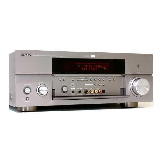
Page 3: Front Panels
RX-V1700/DSP-AX1700 I FRONT PANELS RX-V1700 (U, C models) RX-V1700 (R, T, K, A, B, G, E, L models) DSP-AX1700 (J model) -
Page 4: Rear Panels
RX-V1700/DSP-AX1700 I REAR PANELS RX-V1700 (U, C models) RX-V1700 (R model) RX-V1700 (T model) - Page 5 RX-V1700/DSP-AX1700 RX-V1700 (K model) RX-V1700 (A model) RX-V1700 (B model)
- Page 6 RX-V1700/DSP-AX1700 RX-V1700 (G, E models) RX-V1700 (L model) DSP-AX1700 (J model)
-
Page 7: Remote Control Panels
RX-V1700/DSP-AX1700 I REMOTE CONTROL PANELS RX-V1700 (U, C models) RX-V1700 (R, T, K, A, B, G, E, L models) DSP-AX1700 (J model) RX-V1700 (U, C models) RX-V1700 (R, T, K, A, B, L models) -
Page 8: Specifications
RX-V1700/DSP-AX1700 I SPECIFICATIONS I Audio Section / Minimum RMS Output Power (Power Amp. Section) / Signal to Noise Ratio / (IHF-A network) (20 Hz to 20 kHz) PHONO (MM) (Input shorted) to SP OUT FRONT L/R U, C, R, T, K, L models (5 mV) ....... 86 dB or more U, C, R, T, K, A, B, G, E, L models (0.04 % THD, 8 ohms) - Page 9 K model ..............AC 220 V, 60 Hz A model ..............AC 240 V, 50 Hz “SILENT CINEMA” is a trademark of YAMAHA CORPORATION. B, G, E models ............AC 230 V, 50 Hz J model ............AC 100 V, 50/60 Hz...
- Page 10 RX-V1700/DSP-AX1700...
-
Page 11: Internal View
RX-V1700/DSP-AX1700 I INTERNAL VIEW RX-V1700/DSP-AX1700 • Top view Power Transformer POWER (4) P.C.B. POWER (2) P.C.B. (R, L models) TUNER MAIN (2) P.C.B. FL (3) P.C.B. FL (5) P.C.B. FL(6) P.C.B. FL(4) P.C.B. A-VIDEO P.C.B. FL (2) P.C.B. D-VIDEO P.C.B. -
Page 12: Disassembly Procedures
RX-V1700/DSP-AX1700 I DISASSEMBLY PROCEDURES (Remove parts in the order as numbered.) Disconnect the power cable from the AC outlet. 1. Removal of Top Cover a. Remove 2 screws (1), 4 screws (2) and 5 screws (3). (Fig. 1) b. Slide the top cover rearward to remove it. (Fig. 1) 2. - Page 13 RX-V1700/DSP-AX1700 A-VIDEO P.C.B. Side plate L Sub chassis unit D-VIDEO P.C.B. Side plate R Fig. 2 CB204 CB203 CB953 CB957 CB23 CB136 CB970 CB12 CB807 CB806 CB805 CB971 Fig. 3...
- Page 14 RX-V1700/DSP-AX1700 When checking the P.C.B.: • Place the sub chassis unit on top of the rubber sheet and cloth. (Fig. 4) • Reconnect all cables (connectors) that have been dis- connected. Be sure to use the extension cable before servicing the following section.
- Page 15 RX-V1700/DSP-AX1700 U, C, R, T, K, A, B, G, E, L models When checking the P.C.B.: • Put the rubber sheet and cloth over the equipment. (R, L models) Then place the P.C.B.s upside down on the cloth and check it. (Fig. 6) •...
- Page 16 RX-V1700/DSP-AX1700 6. Removal of Rear Unit FUNCTION (1) P.C.B. Rear unit a. Remove 11 (U, C, T, A, B, G, E models) / 13 (R, L mod- DSP P.C.B. els) screws (C) and 4 (U, C, R, T, A, B, G, E, L models) MF126500 / 2 (K model) screws (D).
- Page 17 RX-V1700/DSP-AX1700 When checking the Amp Unit: • Place the sub chassis unit on top of the rubber sheet and cloth. (Fig. 10) • Put the amp unit together with the heat sink upright and check. (Fig. 10) • Reconnect all cables (connectors) that have been dis- connected.
-
Page 18: Updating Firmware
RX-V1700/DSP-AX1700 I UPDATING FIRMWARE / When replacing the following parts, be sure to write the latest firmware. IC540 of DSP P.C.B. : X8012A00 IC402 of FUNCTION P.C.B.: X8337A00 IC147 of D-VIDEO P.C.B. : X8069A00 G Required tools • DVD or CD player (with DIGITAL OUTPUT (OPTI- CAL or COAXIAL) terminal) •... - Page 19 RX-V1700/DSP-AX1700 2. Reconnect the power cable of main unit to the AC 11. Press the “STOP” key of the DVD/CD player. outlet. 12. Press the “EJECT” key of the DVD/CD player to 3. Reconnect the power cable of DVD/CD player to open the tray.
- Page 20 RX-V1700/DSP-AX1700 I SELF DIAGNOSIS FUNCTION (DIAG) No DIAG MENU SUB MENU INPUT SELECT 7. MODEL – 8. DESTINATION – There are 29 DIAG menu items, each of which has sub- 9. PANEL KEY (K0/K1) – menu items. Listed in the table below are menu items and 12 XM TEST TONE 1.
- Page 21 RX-V1700/DSP-AX1700 No DIAG MENU SUB MENU INPUT SELECT 3. HDMI I/P – 4. HDMI 720p ( – Not applied to these models. / 5. HDMI 1080p ( – Not applied to these models. / 6. HDMI SMART ZOOM ( –...
- Page 22 RX-V1700/DSP-AX1700 • Starting DIAG Press the “MASTER ON/OFF” key while simultaneously pressing those two keys of the main unit as indicated in the figure below. Keys of main unit Turn on the power while pressing these keys. • Starting DIAG in the protection cancel...
- Page 23 RX-V1700/DSP-AX1700 • Display provided when DIAG started The FL display of the main unit displays the protection function history data and the version (1 alphabet) then the DIAG menu (sub-menu of DIAG menu No.1 DA70Y-YSS930) a few seconds later. When there is no history of protection function:...
- Page 24 RX-V1700/DSP-AX1700 When there is a history of protection function due to abnormal voltage in the power supply section Version (1 alphabet) PSx PRT:000 Z A/D conversion value of voltage Cause: The voltage in the power supply section is abnormal. Supplementary information: The abnormal voltage is displayed in based on 5V as 255.
- Page 25 RX-V1700/DSP-AX1700 • History of protection function When the protection function has worked, its history is stored in memory with a backup. Even if no abnormality is noted while servicing the unit, an abnormality which has occurred previously can be defined as long as the backup data has been stored.
- Page 26 RX-V1700/DSP-AX1700 • Functions in DIAG mode In addition to the DIAG menu items, functions listed below are available. • Input selection, Multi channel input • Center/Rear/Rear center/Sub-woofer level adjustment • Muting • Power on/off • Master volume Functions related to the tuner and the set menu are not available.
- Page 27 RX-V1700/DSP-AX1700 • Details of DIAG menu With full-bit output specified in some modes, it is possible to execute 0dBFS output without head margin in each channel. 1. DA70Y-YSS930 This function is for YSS930 only. Main DSP of YSS930 is selected for FRONT output.
- Page 28 RX-V1700/DSP-AX1700 2. BYPASS ANALOG BYPASS 2.BYPASS ANALOG BYPASS INPUT: DVD ANALOG SPEAKER OUT: 1kHz, SUBWOOFER OUTPUT: 50Hz SPEAKER OUT SUBWOOFER Input level Volume OUTPUT FRONT CENTER SURROUND SURROUND BACK PRESENCE Both ch, -20 dBm +6.5 dB +12.5 dBm -∞ -∞...
- Page 29 RX-V1700/DSP-AX1700 3. RAM THROUGH Using the sub-menu, it is possible to select the full-bit output at 0dB output level. MARGIN 3.RAM THROUGH MARGIN INPUT: DVD ANALOG SPEAKER OUT: 1kHz, SUBWOOFER OUTPUT: 50Hz SPEAKER OUT SUBWOOFER Input level Volume OUTPUT FRONT...
- Page 30 RX-V1700/DSP-AX1700 4. HDMI AUDIO The signals input to HDMI IN1 and IN2 are selected by the sub-menu and output. SPDIF Only SPDIF is output. SPDIF Multi Only Multi (DVD-AUDIO) is output. Multi Not applied to these models. DSD Direct Not applied to these models.
- Page 31 RX-V1700/DSP-AX1700 The analog switch settings for each sub-menu are as shown in the table below. SUB MENU FL/FR CENTER SL/SR SBL/SBR LFE/BASS 1. FRONT: SMALL 0dB SMALL LARGE LARGE LARGE SWFR 2. LFE/B: FRNT LARGE LARGE LARGE LARGE FRONT 3. Pres Mix: 5ch...
- Page 32 RX-V1700/DSP-AX1700 6. MULTI CH INPUT It is possible to select the 6ch/8ch input and 6-ohm/8- ohm by using the SUB menu. 6CH INPUT_6-ohm 6.Multi INPUT 6ch INPUT_6 INPUT: MULTI CH INPUT SPEAKER OUT: 1kHz, SUBWOOFER OUTPUT: 50Hz SPEAKER OUT SUBWOOFER...
- Page 33 RX-V1700/DSP-AX1700 TMP TEST/AMP. POWER CONTROL From the power relay of the amplifier section. Use the “STRAIGHT” key to change operation. 6.Multi INPUT 255000053053:H Display RY250 (MAIN P.C.B.) RY251 (MAIN P.C.B.) H (HIGH) M (MID) L (LOW) 7. MIC CHECK The signals input through the microphone are output via A/D - D/A.
- Page 34 RX-V1700/DSP-AX1700 8. FL/OSD CHECK Use this program to check the FL display section and image control section. When checking the image con- trol section, prepare a monitor, HDMI cable, compo- nent video cable, S video cable and video pin cable and connect them.
- Page 35 RX-V1700/DSP-AX1700 Check of the Video control circuit. (Monitor out) / The image signal is output as follows. Initial display/Video conversion ON Video conversion ON Input Output HDMI COMPONENT VIDEO S VIDEO VIDEO Through Video conversion Component interlace/progressive up-conversion HDMI interlace/progressive...
- Page 36 RX-V1700/DSP-AX1700 9. MANUAL TEST The noise generator with a built-in DSP outputs the test noise through the channels specified by the sub- menu. The noise frequency for LFE is 30 to 80 Hz. Other than that, the noise frequency is 500 to 2 kHz.
- Page 37 RX-V1700/DSP-AX1700 HARD FLOW This sub-menu is used to check operation of the flow port of the hardware. “OK” appears when the check result is satisfactory and “NG” when it is not. 10.RS-232C HARD FLOW: 11.AD DATA CHECK This menu is used to display the A/D conversion value...
- Page 38 RX-V1700/DSP-AX1700 TM1/TM2 (temperature detection) Temperature detected value (Normal value: 10 to 83) (Normal value: 10 to 78) L model TM1: Detects the temperature of the heat sink at the left side (power transformer side) TM2: Detects the temperature of the heat sink at the right...
- Page 39 ±4. In this case, check the constant of partial pressure resistor, solder condition, etc. Refer to table. (Reference voltage: 5V=255) 11.AD CHECK K0:255 K1:255 RX-V1700 (U, C, R, T, K, A, B, G, E, L models) DSP-AX1700 (J model) Display KEY0 KEY1 Display...
- Page 40 RX-V1700/DSP-AX1700 12.XM STATUS (U, C models) The output check of XM Radio Antenna is executed. 1k -1dB/44.1k The test tone (1kHz, -1dB/44.1kHz) is output. 12.XM STATUS 1k - 1dB/44 1k -61dB/44.1k The test tone (1kHz, -61dB/44.1kHz) is output. 12.XM STATUS 1k -61dB/44 Mute /44.1k...
- Page 41 RX-V1700/DSP-AX1700 ISO Tone/32k The ISO tone (32kHz) is output. 12.XM STATUS ISO Tone/32 XM/DT Bus Power: OFF The power of XM module is turned off. 12.XM STATUS Bus Power:OFF 13.IF STATUS (Input function status) Using the sub-menu, the status data is displayed one after another in the hexadecimal notation.
- Page 42 RX-V1700/DSP-AX1700 <4th byte> Format information of reproduction signal *1: Analog processing used for digital reproduction is not possible because of a commercial bit or 4-ch audio reason. Display Signal format Analog (Unlock) Incorrect Digital (*1) PCM Audio Digital Data IEC1937 Data...
- Page 43 RX-V1700/DSP-AX1700 14.iPod This menu is used to test the DOCK connector without the iPod itself. After turning off the power, short be- tween pins No. 14 (TX) and No. 18 (RX), between pins No. 1 (PWR) and No. 17 (ACCPOW) and between pins No.
- Page 44 RX-V1700/DSP-AX1700 15.NET CHECK Not applied to these models. IP Address Check 15.NET CHECK IP CHECK: MAC Address Check 15.NET CHECK MAC CHECK: 16.USB CHECK Not applied to these models. USB 1track 16.USB CHECK USB 1 TRACK USB 2track 16.USB CHECK...
- Page 45 RX-V1700/DSP-AX1700 17.PROTECTION HIST. The history of protection function is displayed. After selecting the sub-menu, press the “STRAIGHT” key, and the history will be erased. Last 17.PRTCT HIST. LAST :NO PROT History1 17.PRTCT HIST. Hist1:NO PROT History2 17.PRTCT HIST. Hist2:NO PROT History3 17.PRTCT HIST.
- Page 46 Not applied to these models. 19.DVIDEO CHK YGV:NoError 20.HDMI INFORMATION HDMI Model Name The model name of this unit written in HDMI module is displayed. RX-V1700 (U, C, R, T, K, A, B, G, E, L models) DSP-AX1700 (J model) 20.HDMI INFO HMN:DSP-AX1700...
- Page 47 310A (U, C, R, T, K, A, B, G, L models) 3109 (J model) 20.HDMI INFO HPI:3109 HDMI Vendor Name The vendor name (YAMAHA) of this unit written in the HDMI module is displayed. 20.HDMI INFO HVN:YAMAHA 21.HDMI SELECT HDMI NONE: No Connect Neither HDMI IN 1 terminal nor HDMI IN 2 terminal is se- lected for input.
- Page 48 RX-V1700/DSP-AX1700 22.HDMI UPCONV The image signal is converted and output to HDMI OUT as follows. HDMI Decoder 22.HDMI UPCONV HDMI DECODER HDMI YGV Not applied to these models. 22.HDMI UPCONV HDMI YGV HDMI I/P 22.HDMI UPCONV HDMI I/P HDMI 720p Not applied to these models.
- Page 49 RX-V1700/DSP-AX1700 23.VIDEO The image signal is converted and output as follows. DIGITAL THR COMP 23.VIDEO DIGITAL COMP DIGITAL THR CVBS 23.VIDEO DIGITAL CVBS DIGITAL THR Y/C 23.VIDEO DIGITAL Y/C...
- Page 50 RX-V1700/DSP-AX1700 DIGITAL BYPASS 23.VIDEO DIGITAL BYPASS ANALOG BYPASS 23.VIDEO ANALOG BYPASS TEST PATTERN 1 23.VIDEO TEST PATTERN 1...
- Page 51 RX-V1700/DSP-AX1700 TEST PATTERN 2 23.VIDEO TEST PATTERN 2 VIDEO INFO Displays the information of image signals being input. 23.VIDEO VIDEO IN ---- 24.ACCESS CHECK Not applied to these models. TI FLASH READ 24.BUS CHECK TI FLASH R TI FLASH WRITE 24.BUS CHECK...
- Page 52 RX-V1700/DSP-AX1700 25.Firm UPDATE Select this when writing the firmware. (Not applied to these models.) 232C MAIN Writing of MAIN. 25.FLASH 232C MAIN 232C VIDEO Writing of VIDEO. 25.FLASH 232C VIDEO 232C TI Writing of DSP. 25.FLASH 232C USB NET 25.FLASH 232C NET/USB UPDATE 26.SET INFO...
- Page 53 RX-V1700/DSP-AX1700 27.SOFT SW RDS EXIST: EXIST/NOT This menu is used to switch the function settings on EXIST or NOT can be selected. P.C.B. through the software so as to activate the prod- EXIST (B, G, E models) uct. (U, C, R, T, K, A, L, J models) The protection function follows the P.C.B.
- Page 54 RX-V1700/DSP-AX1700 28.FACTORY PRESET 29.ROM VER/SUM This menu is used to reserve and inhibit initialization of The version and checksum are displayed. The signal is the back-up RAM. The signals are processed using processed using EFFECT OFF. The checksum is ob- EFFECT OFF.
-
Page 55: Amp Adjustment
RX-V1700/DSP-AX1700 I AMP ADJUSTMENT FRONT Confirmation of Idling Current of Amp Unit • Right after power is turned on, confirm that the voltage FRONT Rch across the terminals of R CENTER FRONT Lch SURROUND R468 ( ), R469 (FRONT Rch), R470... -
Page 56: Display Data
RX-V1700/DSP-AX1700 I DISPLAY DATA G V9001 : HNA-16ML12T (WH303800) G ANODE CONNECTION 1GA-14GA 15GA 16GA 1GB-14GB 15GB 1-1A 1-1B 2-1A 2-1B PATTERN AREA 3-1A 3-1B 4-1A 4-1B 5-1A 5-1B 1-2A 1-2B G PIN CONNECTION 2-2A 2-2B 3-2A 3-2B Pin No. - Page 57 RX-V1700/DSP-AX1700 I IC DATA IC148: M30845MW-001-GP (D-VIDEO P.C.B) Single chip 16/32-bit microprocessor Port P0 Port P1 Port P2 Port P3 Port P4 Port P5 Port P6 < > < > Peripheral Functions Clock Generation Circuit A/D Converter: 1 circuit Timer (16 bits)
- Page 58 RX-V1700/DSP-AX1700 IC148: M30845MW-001-GP (D-VIDEO P.C.B) Single chip 16/32-bit microprocessor Terminal Name Port Name Port I/O Function (P.C.B.) P96/SDA4 SDAL I/O signal of I2C SDA (for 100kHz device) P95/CLK4 P94/DA1/TB4in LPFCTL LPF fs select P93/TB3in CEC5A HDMI CEC spare P92/SDA3 SDAH...
- Page 59 RX-V1700/DSP-AX1700 IC148: M30845MW-001-GP (D-VIDEO P.C.B) Single chip 16/32-bit microprocessor Terminal Name Port Name I/O [OFF] Function (P.C.B.) P132 DDCENB HDMI DDC enable control Vcc2 3.3V 3.3V P131 PWRENB Whether to connect +5V of Source and RX or not P130 HPDENB...
- Page 60 RX-V1700/DSP-AX1700 IC148: M30845MW-001-GP (D-VIDEO P.C.B) Single chip 16/32-bit microprocessor Terminal Name Port Name I/O [OFF] Function (P.C.B.) P110 /ICV /IC signal to VDEC/VENC P03/D3 Data bus P02/D2 Data bus P01/D1 Data bus P00/D0 Data bus P157 /AUPS Video passage to HDMI (scaler output) ON/OFF...
- Page 61 RX-V1700/DSP-AX1700 IC402: M30845FJGP (FUNCTION P.C.B) Single chip 16/32-bit microprocessor Port P0 Port P1 Port P2 Port P3 Port P4 Port P5 Port P6 < > < > Peripheral Functions Clock Generation Circuit A/D Converter: 1 circuit Timer (16 bits) Standard: 10 inputs...
- Page 62 RX-V1700/DSP-AX1700 IC402: M30845FJGP (FUNCTION P.C.B) Single chip 16/32-bit microprocessor Terminal Name Port Name Port I/O Function (P.C.B.) TXD4 TXDH Data transmission to VIDEO_CPU CLK4 CLKH Clock transmission to VIDEO_CPU LMTCNT Limiter control output TB3in/DA0 HDMINT HDMI MUTE input SDA3/TXD3/TB2in TXDi...
- Page 63 RX-V1700/DSP-AX1700 IC402: M30845FJGP (FUNCTION P.C.B) Single chip 16/32-bit microprocessor Terminal Name Port Name I/O [OFF] Function (P.C.B.) P133 CKZEV ZONE tone control IC serial transmission clock (U, C, R, T, K, A, B, G, E, L models) P132 DTZEV ZONE tone control IC serial transmission data (U, C, R, T, K, A, B, G, E, L models)
- Page 64 AD power limiter output level detect Vref VREF Avcc AVCC RXD4 RXDH Data reception from VIDEO_CPU RX-V1700 (U, C, R, T, K, A, B, G, E, L models) Key input(A-D) pull-up resistance 10 k-ohms +1.2k +1.2k +1.8k +2.7k +3.3k +4.7k +8.2k...
- Page 65 RX-V1700/DSP-AX1700 IC534: D70YE101RFP250 (DSP P.C.B.) Decoder/Post processor No replacement part available. SPI0_SIMO EM_CKE SPI0_SOMI/I2C0_SDA EM_CLK AXR0[0] EM_WE_DQM[1] AXR0[1] EM_D[8] AXR0[2] AXR0[3] EM_D[9] EM_D[10] AXR0[4] AXR0[5]/SPI1_SCS EM_D[11] AXR0[6]/SPI1_ENA AXR0[7]/SPI1_CLK EM_D[12] EM_D[13] EM_D[14] AXR0[8]/AXR1[5]/SPI1_SOMI EM_D[15] AXR0[9]/AXR1[4]/SPI1_SIMO EM_D[0] AXR0[10]/AXR1[3] EM_D[1] AXR0[11]/AXR1[2] EM_D[2] EM_D[3]...
- Page 66 RX-V1700/DSP-AX1700 IC534: D70YE101RFP250 (DSP P.C.B.) Decoder/Post processor PIN NO. SIGNAL NAME TYPE PULL GPIO DESCRIPTION Ground(Vss) AHCLKX0/AHCLKX2 McASP0 and McASP2 transmit master clock AMUTE0 McASP0 mute output AMUTE1 McASP1 mute output AHCLKX1 McASP1 transmit master clock Ground(Vss) ACLKX1 McASP1 transmit bit clock...
- Page 67 RX-V1700/DSP-AX1700 IC534: D70YE101RFP250 (DSP P.C.B.) Decoder/Post processor PIN NO. SIGNAL NAME TYPE PULL GPIO DESCRIPTION EM_D[14] EMIF data bus [lower 16-Bits] Core Supply (CVpp) EM_D[13] EMIF data bus [lower 16-Bits] EM_D[12] EMIF data bus [lower 16-Bits] IO Supply (DVpp) EM_D[11]...
- Page 68 RX-V1700/DSP-AX1700 IC534: D70YE101RFP250 (DSP P.C.B.) Decoder/Post processor PIN NO. SIGNAL NAME TYPE PULL GPIO DESCRIPTION SPI0_SOMI/I2C0_SDA SPI0 data pin slave out master in or I2C0 serial data IO Supply (DVpp) AXR0[0] McASP0 serial data 0 Ground(Vss) AXR0[1] McASP0 serial data 1...
- Page 69 RX-V1700/DSP-AX1700 I BLOCK DIAGRAMS AUDIO SECTION BLOCK DIAGRAM IN 1 • See page 103-105 → D-VIDEO MPCM EQUALIZER IC101 SCHEMATIC DIAGRAM 1442 Sil9033 • See page 115-116 → IC103 IN 2 CBL/SAT IC503 SCHEMATIC DIAGRAM DSD Direct EQUALIZER 1442 IC102...
- Page 70 RX-V1700/DSP-AX1700 VIDEO SECTION BLOCK DIAGRAM HDMI HDMI D-VIDEO Pb/Cb MONITOR OUT Pr/Cr • See page 115-116 → A-VIDEO SCHEMATIC DIAGRAM • See page 113-114 → SCHEMATIC DIAGRAM POWERSAVE /VMT MONITOR OUT /MTMON Pb/Cb IC203 D5 VIDEO Pr/Cr NJM2581 L1/L2/L3 (J model)
- Page 71 RX-V1700/DSP-AX1700 CONTROL/POWER SUPPLY SECTION BLOCK DIAGRAM • See page 112 → POWER Power Transformer SCHEMATIC DIAGRAM RY251 RY250 AC IN • See page 111 → MAIN SCHEMATIC DIAGRAM 2SD2014 2SD2014 +5D2 POWER POWER DETECT DETECT IC1,2,3 /RESET RESET Q1,3 2SB1257 FUNCTION •...
- Page 72 RX-V1700/DSP-AX1700 I PRINTED CIRCUIT BOARDS DIGITAL INPUT DIGITAL OUTPUT DSP P.C.B. (Side A) COAXIAL OPTICAL U, C models DOCK DVR/VCR 2 CBL/SAT MD/TAPE CD-R OPERATION (3) (CB805) DGND +5D1 FL (5) (CB959) • Semiconductor Location FL (2) Ref no. Location Ref no. Location...
- Page 73 RX-V1700/DSP-AX1700 DSP P.C.B. (Side B) U, C models • Semiconductor Location Ref no. Location Ref no. Location D5300 D5602 D5301 D5603 D5302 D5604 D5303 D5605 D5306 D5606 D5308 D5607 D5309 Q5001 D5311 Q5002 D5600 Q5301 D5601 Circuit No. U, C...
- Page 74 RX-V1700/DSP-AX1700 Circuit No. U, C, R, T, K, A, B, G, E, L C4064 C4065 C4530, 4533 FUNCTION (1) P.C.B. (Side A) C4523, 4528 IC450 J4506, 4507 VIDEO (AUDIO) J4510, 4511 U, C, R, T, K, A, B, G, E, L models...
- Page 75 RX-V1700/DSP-AX1700 FUNCTION (1) P.C.B. (Side B) J model U, C, R, T, K, A, B, G, E, L models U, C, R, T, K, A, B, G, E, L models • Semiconductor Location Ref no. Location Ref no. Location D4004...
- Page 76 RX-V1700/DSP-AX1700 FUNCTION (2) P.C.B. (Side A) Circuit No. U, C R, T, K, A, B, G, E, L C3601, 3610 IC310, 311 U, C, R, T, K, A, B, G, E, L models IC356 AUDIO MULTI CH INPUT PRE OUT...
- Page 77 RX-V1700/DSP-AX1700 FUNCTION (2) P.C.B. (Side B) Circuit No. U, C, R, T, K, A, B, G, E, L J3550, 3551 X : NOT USED O : USED/APPLICABLE R, T, K, A, B, G, E, L models • Semiconductor Location Ref no. Location...
- Page 78 RX-V1700/DSP-AX1700 OPERATION (1) P.C.B. OPERATION (2) P.C.B. (Side A) (Side A) • Semiconductor Location Ref no. Location D8001 FL (1) (W9004) (RESET) PURE DIRECT VOLUME MAIN ZONE ON/OFF INPUT FL (2) (CB971)
- Page 79 RX-V1700/DSP-AX1700 OPERATION (2) P.C.B. OPERATION (1) P.C.B. (Side B) (Side B) • Semiconductor Location Ref no. Location Q8001...
- Page 80 RX-V1700/DSP-AX1700 OPERATION (3) P.C.B. (Side A) VIDEO AUX OPTIMZER PHONES S-VIDEO VIDEO AUDIO OPTICAL OPERATION (4) (CB810) +5D1 FUNCTION (2) (W301B) A-VIDEO (W5001) (W2002) OPERATION (4) P.C.B. OPERATION (5) P.C.B. (Side A) (Side A) FL (1) FL (1) (W9003) (W9002) •...
- Page 81 RX-V1700/DSP-AX1700 OPERATION (3) P.C.B. (Side B) OPERATION (5) P.C.B. OPERATION (4) P.C.B. (Side B) (Side B) • Semiconductor Location Ref no. Location Ref no. Location D8004 D8010 D8005 IC801 D8006 IC802 D8007 IC805 D8008 Q8002 D8009 Q8003 Circuit No. U, C, J...
- Page 82 RX-V1700/DSP-AX1700 MAIN (1) P.C.B. (Side A) MAIN (2) (W256B) MAIN (2) (W252B)(W252D) MAIN (2) (W253B)(W253D) BLUE BROWN MAIN (4) BLACK (W250B) MAIN (4) YELLOW (W260B) MAIN (3) GRAY (W259B) + LB MAIN (4) (W274A) POWER (3) (CB19) MAIN (4) MAIN (3)
- Page 83 RX-V1700/DSP-AX1700 MAIN (1) P.C.B. (Side B) • Semiconductor Location Ref no. Location Ref no. Location Ref no. Location Ref no. Location Ref no. Location Ref no. Location D252 D270 D289 Q250 Q262 Q317 D253 D271 D290 Q251 Q263 Q318 D254...
- Page 84 RX-V1700/DSP-AX1700 MAIN (4) P.C.B. (Side A) MAIN (2) P.C.B. MAIN (3) P.C.B. (Side A) (Side A) MAIN (1) (W274B) MAIN (1) MAIN (4) (W255A) (W263A) CGND U, C, R, T, K, A, B, G, E, L models BLACK R596 D304...
- Page 85 RX-V1700/DSP-AX1700 MAIN (4) P.C.B. (Side B) MAIN (2) P.C.B. MAIN (3) P.C.B. (Side B) (Side B) U, C, T, K, A, B, G, E, L models U, C, T, K, A, B, G, E, L models • Semiconductor Location Ref no. Location Ref no. Location...
- Page 86 RX-V1700/DSP-AX1700 POWER (1) P.C.B. POWER (1) P.C.B. (Side A) (Side B) POWER TRANSFORMER POWER (3) (W7A) +5D1 FL (1) (W9001) +5D1 /VPOWER POWER (3) (W3A) POWER (3) (W8A) • Semiconductor Location Ref no. Location...
- Page 87 RX-V1700/DSP-AX1700 POWER (2) P.C.B. (Side A) POWER (6) P.C.B. (Side A) R, L models POWER TRANSFORMER POWER (4) (CB6) • Semiconductor Location Ref no. Location IC13 IC14 POWER TRANSFORMER POWER (5) P.C.B. (Side A) POWER (3) (W5A) POWER (5) P.C.B.
- Page 88 RX-V1700/DSP-AX1700 POWER (3) P.C.B. (Side A) POWER (1) POWER (1) (W8B) (W7B) POWER TRANSFORMER D-VIDEO (CB136) DVGNDsens POWER (1) +3.3VD (W3B) +5VD +BDV +5SDV DVGReturn DVGReturn +BAV -BAV VAGsens +6SDSP DGReturn POWER (5) (W5B) FUNCTION (1) FUNCTION (2) MAIN (4)
- Page 89 RX-V1700/DSP-AX1700 POWER (4) P.C.B. POWER (4) P.C.B. (Side A) (Side B) POWER (2) (W2A)(W2B) (R model) POWER TRANSFORMER (U, C, T, K, A, B, G, E, J models) /RES PDET /LFAN • Semiconductor Location Ref no. Location Ref no. Location Circuit No.
- Page 90 RX-V1700/DSP-AX1700 • Semiconductor Location Ref no. Location Ref no. Location Ref no. Location Ref no. Location D2001 D2009 IC211 IC223 D2002 IC201 IC213 IC224 D2003 IC202 IC215 IC225 A-VIDEO P.C.B. (Side A) D2004 IC203 IC218 Q2601 D2005 IC204 IC219 Q2632...
- Page 91 RX-V1700/DSP-AX1700 A-VIDEO P.C.B. (Side B) • Semiconductor Location Ref no. Location Ref no. Location D2061 D2633 Circuit No. U, C, J R, T, K, A, B, G, E, L D2062 D2634 C2501-2504 D2561 Q2541 J2501-2504 D2563 Q2542 X : NOT USED...
- Page 92 RX-V1700/DSP-AX1700 • Semiconductor Location Ref no. Location Ref no. Location Ref no. Location Ref no. Location Ref no. Location Ref no. Location Ref no. Location Ref no. Location Ref no. Location D1011 D1021 D1031 D1503 IC106 IC133 IC146 IC175 Q1503...
- Page 93 RX-V1700/DSP-AX1700 • Semiconductor Location D-VIDEO P.C.B. (Side B) Ref no. Location Ref no. Location D1065 IC180 D1504 Q1014 D1505 Q1015 D1506 Q1016 D1512 Q1017 D1514 Q1018 D1515 Q1513 D1516...
- Page 94 RX-V1700/DSP-AX1700 FL (1) P.C.B. FL (1) P.C.B. (Side A) (Side A) POWER (1) (CB12) FL (2) (CB970) OPERATION (5) HPMT (CB809) /MIC KEY1 PSWB PSWA KEY1B +5M2 BT232C KEY0 +5SPC +5D1 REM1 CEF2 CEF1 SCKN SDTN +5M2 /ICFL +5M2 OPERATION (1)
- Page 95 RX-V1700/DSP-AX1700 FL (1) P.C.B. FL (1) P.C.B. (Side B) 48 49 16 17 U, C, R, T, K, A, B, G, E, L models • Semiconductor Location Ref no. Location Ref no. Location D9005 Q9001 D9006 Q9002 D9015 Q9003 D9017...
- Page 96 RX-V1700/DSP-AX1700 FL (2) P.C.B. (Side A) D-VIDEO D-VIDEO (CB138) (CB140) OPERATION (2) (CB803) +5D1 PDLED KEY1B +5SPC +5M2 /RES BOOT TXDF BUSY RXDF HPMT /MIC KEY1 PSWDET PSW2 PSW1 KEY1B BT232C KEY0 +5SPC REM1 CEF2 CEF1 SCKN SDTN /ICFL +5M2...
- Page 97 RX-V1700/DSP-AX1700 FL (2) P.C.B. (Side B)
- Page 98 RX-V1700/DSP-AX1700 FL (3) P.C.B. FL (4) P.C.B. (Side A) (Side A) FUNCTION (1) (CB404) FUNCTION (2) (CB403) INPR INPR INPL INPL TPRR TPRR TPRL TPRL NETR NETR NETL NETL Z2R1 Z2R1 Z2L1 Z2L1 FUNCTION (2) FUNCTION (1) (CB453) (CB351) FUNCTION (2)
- Page 99 RX-V1700/DSP-AX1700 FL (5) P.C.B. (Side A) FL (6) P.C.B. (Side A) U, C, R, T, K, A, B, G, E, L models CONTROL OUT RS-232C +12V 15mA MAX. /INTDIR /INTDIR /CSY /CSY /INTTI /INTTI SPIRDY SPIRDY /ICTI /ICTI /CSTI /CSTI...
- Page 100 RX-V1700/DSP-AX1700 I PIN CONNECTION DIAGRAMS • ICs ADM222ARZ ADV7322KSTZ ADV7401BSTZ-80 AK4384ET BA00JC5WT-V5 CD4051BNSR NJM2581M NJM2845DL1-18 NJM2867F3-05 NJM2885DL1-25 2:GND NJU7311AM NJW1119V NJM2885DL1-33 NJM4565M NJU7312AM NJU7313AM 2:GND BA15218F BD3841FS CBX1442R DSD1791DBR F2602E-01 1:IN 3:OUT NJW1321FP1 PCM1804DBR PQ200WNA1ZPH PT6302LQ KIA7809API-U/P KIA79M05PI-U LA7106M-TLM-E LA73050-TLM-E...
- Page 101 RX-V1700/DSP-AX1700 SN74CBT3257CPWR SN74LV157APWR SN74LV245APWR SN74LVC32APWR SN74LS151NSR SN74LVU04APWR SN74LVC245APWR SN74LVC2G02DCTR SN74LVC2G125DCUR TA1318AF SN74LVC3G04DCTR TK15420M µPC4570G2 TC4013BP TC74HC4052AF TC74VHCU04FT TLP421 TC74VHC153FT W9816G6CH-7 YAC523-EVR2 YAC526-EZE2 YSS930B-SZ...
- Page 102 RX-V1700/DSP-AX1700 • Diodes 1N4002S 1SS355 MA8240-M 1SS133,176 1SS380 MA8300-L HZS242TD MA8030-L RB051L-40 MTZJ10B MA-8039-H RB501V-40 MTZJ5.1C MA8043-L RB551V-30 MTZJ6.8B MA8047 UDZS5.6BTE-17 Anode MA8047-L Anode MA8051-M MA8062-M MA8068-M Cathode MA8075-M MA8130-M Cathode D15XB20 D2SBA20 D4SBS4-4101 RLS245 RS1503M Anode – – Cathode DB105 –...
- Page 103 RX-V1700/DSP-AX1700 SCHEMATIC DIAGRAMS DSP 1/3 IC501: SN74LVU04APWR IC502: SN74AHCT00PWR Hex inverters Quadruple 2-input NAND gate Page 106 Page 110 Page 118 to FUNCTION (1)_CB411 to OPERATION (3)_CB805 to FL (2)_CB954 IC503, 509: SN74LV157APWR DOCK Quadruple 2-line to 1-line data selectors/multiplexers...
- Page 104 RX-V1700/DSP-AX1700 DSP 2/3 Page 118 Page 118 Page 112 Page 112 to FL (5)_CB973 to FL (5)_CB959 to POWER (3)_CB16 to POWER (3)_CB17 IC531: SN74AHC1G08DCKR IC532, 533: SN74AHCT1G32DCKR 2-input positive-AND gate Single 2-input positive-OR gate IC535: SN74AHCT08PWR Quadruple 2-input positive-AND gates U, C models -0.1...
- Page 105 RX-V1700/DSP-AX1700 DSP 3/3 IC550, 552: YSS930B-SZ Page 108 to FUNCTION (2)_CB300 12.0 ANALOG IN MICROPROCESSOR INTERFACE PROGRAM COEFFICIENT ADDRESS CONTROL REGISTER 50 bit 1024 16 bit 1024 17 bit FRONT L CONTROL SIGNALS SDBCK SDWCK 12.2 SDI0 SDO0 U, C models...
- Page 106 RX-V1700/DSP-AX1700 FUNCTION 1/4 IC401: LC72722PM RDS signal processor VDDA CLOCK VDDD RECOVERY REFERENCE (57 kHz) (1187.5 Hz) VOLTAGE VSSA VSSD VREF 57 kHz ANTIALIASING SMOOTHING DATA MPX IN RDS-ID FILTER FILTER DECODER (SCF) SYNC ERROR CORRECTION SYNC / EC (24 BLOCK DATA)
- Page 107 RX-V1700/DSP-AX1700 FUNCTION 2/4 FUNCTION (1) IC450, 451: BD3841FS Function switch LOGIC INPUT/ZONE3 SELECTOR F-SW1: INPUT FUNCTION 1 F-SW2: INPUT FUNCTION 2 -6.1 Page 118 to FL (4)_CB963 REC/ZONE2 SELECTOR -6.1 # All voltages are measured with a 10MΩ/V DC electronic voltmeter.
- Page 108 RX-V1700/DSP-AX1700 FUNCTION 3/4 FUNCTION (2) IC300: NJU7312AM Analog function switch Page 112 to POWER (3)_CB20 -11.3 11.8 -11.3 11.8 11.8 -11.3 11.8 L-COM1 R-COM1 -6.5 -6.5 -6.1 -11.3 L-COM2 R-COM2 FRONT L 11.8 BYPASS 11.8 L-COM3 R-COM3 DATA -6.1 Control Circuit -11.2...
- Page 109 RX-V1700/DSP-AX1700 FUNCTION 4/4 Page 110 Page 118 to OPERATION (3)_CB806 to FL (2)_CB967 FUNCTION (2) IC350, 351: NJM2068MD-TE2 IC355, 356: BD3841FS Dual operational amplifier Function switch 11.3 –IN – – LOGIC –IN –V -11.8 -6.1 F-SW1: INPUT FUNCTION 1 F-SW2: INPUT FUNCTION 2 To FUNCTION 3/4 -0.2...
- Page 110 RX-V1700/DSP-AX1700 OPERATION to OPERATION (3)_CB804 OPERATION (4) ON/OFF Page 117 IC801: NJM4565M to FL (1)_W9004 Dual operational amplifier Page 103 to DSP_W5001 2, 6 –INPUT OUTPUT 1, 7 +INPUT Page 117 3, 5 to FL (1)_W9003 V– Page 108 to FUNCTION (2)_W301B...
- Page 111 RX-V1700/DSP-AX1700 MAIN -29.9 MAIN (3) SURROUND -62.4 BACK L -29.9 MAIN (2) SURROUND L GRAY CENTER no-use no-use MAIN (4) FRONT L no-use no-use AC74.8 no-use no-use 44.3 -62.2 no-use no-use 62.8 61.8 -61.7 -62.9 AC61.7 62.3 62.4 62.3 -61.9 -63.5...
- Page 112 RX-V1700/DSP-AX1700 POWER IC3: TC4013BP IC1, 2: TLP421 Dual D-type flip flop Photo transistor 19.3 19.1 19.3 RESET1 SET1 19.1 Page 106 Anode Collctor 19.3 to FUNCTION (1)_CB407 DATA1 17.8 Cathode Emitter 19.1 CLOCK1 19.3 17.8 RESET2 19.3 17.8 SET2 19.3 -19.6...
- Page 113 RX-V1700/DSP-AX1700 A-VIDEO 1/2 Page 116 Page 116 A-VIDEO to D-VIDEO_CB132 to D-VIDEO_CB131 IC201: NJW1321FP1 Wide band video switch with I C bus Y/R IN1 Y/R OUT1 Y/R IN2 Y/R IN3 Y/R IN4 J model Y/R OUT2 Pb OUT2 Pr IN4...
- Page 114 RX-V1700/DSP-AX1700 A-VIDEO 2/2 A-VIDEO Page 110 IC218: LA73050-TLM-E IC219: LA7106M-TLM-E to OPERATION (3)_CB807 Analog dual operational amplifier Analog dual operational amplifier N.C. N.C. VIN1+ +VCC N.C. N.C. NFB1 VOUT1 VIN1 +VCC1 MUTE1 +Vcc INPUT SELECTOR DCCNT1 VOUT1 VIN2+ VOUT2 NFB2...
- Page 115 RX-V1700/DSP-AX1700 D-VIDEO 1/2 D-VIDEO EQUALIZER POINT A-3 Pin 96 of IC101 No replacement part available. HDMI DUAL RECEIVER HDMI TRANSMITTER No replacement part available. IC103: CXB1442R IC125: SN74CBT3253CPWR IC122, 124: SN74CBT3257CPWR IC106, 111: SN74LVC245APWR IC108: NJM2867F3-05 (TE-1) IC123: M24C02-WMN6TP IC121: SN74LVC32A...
- Page 116 RX-V1700/DSP-AX1700 D-VIDEO 2/2 D-VIDEO IC137: ADV7401BSTZ-80 Multiformat SDTV/HDTV video decoder and RGB graphics digitizer SDRAM -4.9 -4.9 POINT A-4 Pin 38 of IC137 -4.9 -4.9 IC163: SN74AHCT08PWR VIDEO ENCODER Quadruple 2-input positive-AND gates POINT B-1 Pin 20 of IC148 De-INTERLACER...
- Page 117 RX-V1700/DSP-AX1700 FL 1/2 11.2 10.5 11.2 10.9 -23.5 -23.4 -25.5 -27.5 -23.5 -20.9 -26.7 -22.9 -27.3 21.4 -27.5 -23.5 -25.3 -21.4 11.2 -27.3 -23.5 -25.3 11.2 10.6 -23.3 10.9 FL DRIVER -27.3 -25.3 -27.3 -27.5 -27.5 -25.3 -27.5 -23.5 -23.3 -21.4...
- Page 118 RX-V1700/DSP-AX1700 FL 2/2 Page 115 Page 116 to D-VIDEO_CB140 to D-VIDEO_CB138 FL (4) Page 104 Page 104 to DSP_CB530 to DSP_CB536 Page 106 Page 106 FL (5) to FUNCTION (1)_CB416 to FUNCTION (1)_CB402 Page 108 Page 108 to FUNCTION (2)_CB301...
-
Page 119: Replacement Parts List
RX-V1700/DSP-AX1700 I REPLACEMENT PARTS LIST • ELECTRICAL COMPONENT PARTS WARNING G Components having special characteristics are marked s and must be replaced with parts having specifications equal to those originally installed. ABBREVIATIONS IN THIS LIST ARE AS FOLLOWS: C.A.EL.CHP : CHIP ALUMI.ELECTROLYTIC CAP L.EMIT... - Page 120 RX-V1700/DSP-AX1700 P.C.B. DSP ✻ New Parts...
- Page 121 RX-V1700/DSP-AX1700 P.C.B. DSP ✻ New Parts...
- Page 122 RX-V1700/DSP-AX1700 P.C.B. DSP ✻ New Parts...
- Page 123 RX-V1700/DSP-AX1700 P.C.B. DSP ✻ New Parts...
- Page 124 RX-V1700/DSP-AX1700 P.C.B. DSP ✻ New Parts...
- Page 125 RX-V1700/DSP-AX1700 P.C.B. DSP and P.C.B. FUNCTION ✻ New Parts...
- Page 126 RX-V1700/DSP-AX1700 P.C.B. FUNCTION ✻ New Parts...
- Page 127 RX-V1700/DSP-AX1700 P.C.B. FUNCTION ✻ New Parts...
- Page 128 RX-V1700/DSP-AX1700 P.C.B. FUNCTION ✻ New Parts...
- Page 129 RX-V1700/DSP-AX1700 P.C.B. FUNCTION ✻ New Parts...
- Page 130 RX-V1700/DSP-AX1700 P.C.B. FUNCTION ✻ New Parts...
- Page 131 RX-V1700/DSP-AX1700 P.C.B. FUNCTION and P.C.B. OPERATION ✻ New Parts...
- Page 132 RX-V1700/DSP-AX1700 P.C.B. OPERATION and P.C.B. MAIN ✻ New Parts...
- Page 133 RX-V1700/DSP-AX1700 P.C.B. MAIN ✻ New Parts...
- Page 134 RX-V1700/DSP-AX1700 P.C.B. MAIN ✻ New Parts...
- Page 135 RX-V1700/DSP-AX1700 P.C.B. MAIN ✻ New Parts...
- Page 136 RX-V1700/DSP-AX1700 P.C.B. MAIN ✻ New Parts...
- Page 137 RX-V1700/DSP-AX1700 P.C.B. POWER ✻ New Parts...
- Page 138 RX-V1700/DSP-AX1700 P.C.B. POWER ✻ New Parts...
- Page 139 RX-V1700/DSP-AX1700 P.C.B. POWER ✻ New Parts...
- Page 140 RX-V1700/DSP-AX1700 P.C.B. POWER and P.C.B. A-VIDEO ✻ New Parts...
- Page 141 RX-V1700/DSP-AX1700 P.C.B. A-VIDEO ✻ New Parts...
- Page 142 RX-V1700/DSP-AX1700 P.C.B. A-VIDEO ✻ New Parts...
- Page 143 RX-V1700/DSP-AX1700 P.C.B. A-VIDEO and P.C.B. D-VIDEO ✻ New Parts...
- Page 144 RX-V1700/DSP-AX1700 P.C.B. D-VIDEO ✻ New Parts...
- Page 145 RX-V1700/DSP-AX1700 P.C.B. D-VIDEO ✻ New Parts...
- Page 146 RX-V1700/DSP-AX1700 P.C.B. D-VIDEO ✻ New Parts...
- Page 147 RX-V1700/DSP-AX1700 P.C.B. D-VIDEO and P.C.B. FL ✻ New Parts...
- Page 148 RX-V1700/DSP-AX1700 P.C.B. FL ✻ New Parts...
- Page 149 RX-V1700/DSP-AX1700 Chip Resistors Chip Resistors The chip resistor is not supplied as a replacement part. * When a chip resistor is necessary, use the following part. AAX60720: CHIP RESISTOR SAMPLE BOOK ✻ New Parts ✻ New Parts...
- Page 150 RX-V1700/DSP-AX1700 • OVERALL ASS’Y T, K, B, G, E models U, C, R, T, K, A, R, L models B, G, E, L models 4 (4) 9 (5) 9 (6) U, C models R, L models 6 (2) 9 (3)
- Page 151 RX-V1700/DSP-AX1700 ✻ New Parts ✻ New Parts...
- Page 152 RX-V1700/DSP-AX1700 • ACCESSORIES U, C models R, T, K, A, B, L models 200-1 201-1 201-1 J, U, C, R, T, L models K, A, B, G, E models L model ✻ New Parts...
- Page 153 RX-V1700/DSP-AX1700 • FRONT PANEL and SUB CHASSIS UNIT 2-55 2-55 2-52 2-26 2-52 2-55 2-55 2-27 2-15 2-14 2-55 2-56 2-25 2-55 2-55 2-52 2-38 2-33 2-36 2-24 2-55 2-22 2-30 2-55 2-55 2-36 2-46 2-32 2-23 2-29 2-31 2-53...
- Page 154 RX-V1700/DSP-AX1700 • AMP UNIT 3-1 (4) 3-1 (3) 3-1 (2) 3-33 3-17 3-33 3-33 3-17 3-33 3-35 3-33 3-33 3-33 3-1 (1) 3-32 3-107 3-25 3-34 3-25 3-22 ✻ New Parts...
- Page 155 RX-V1700/DSP-AX1700 I REMOTE CONTROL • RAV360, RAV361 • SCHEMATIC DIAGRAM • PANELS Vbat Vbat RAV360 RAV361 SOURCE (U, C models) (R, T, K, A, B, G, E, L, J models) spring plus 4 x AAA Batteries 7011 7002 2006 7017...
- Page 156 RX-V1700/DSP-AX1700 • KEY NO. LAYOUT • KEY CODE AREA LEARN MACRO Luminous or AMP Library AMPZ1: 2001 (default) AMP Library AMPZ2: 2002 Label transparent MAIN ZONE2 ZONE3 SYSTM MAIN ZONE2 ZONE3 SYSTM – – – – – – – –...
- Page 157 RX-V1700/DSP-AX1700 • RAV26, RAV27 • SCHEMATIC DIAGRAM • KEY CODE YAMAHA IR CODE TABLE ZONE3 Key Name Code ZONE2 Type B1 ID 1 ID 2 Key No. (ZONE/XM) ZONE 2 ZONE 3 ZONE 2 ZONE 3 7A-B8 7A-B9 7D-2F 7D-30...
- Page 158 RX-V1700/DSP-AX1700...
- Page 159 RX-V1700/DSP-AX1700...
- Page 160 RX-V1700/DSP-AX1700...
- Page 161 RX-V1700/DSP-AX1700 Parts List for Carbon Resistors Value 1/4W Type Part No. 1/6W Type Part No. Value 1/4W Type Part No. 1/6W Type Part No. 1.0 Ω 3100 3100 10 kΩ 7100 7100 HJ35 HF85 HF45 HF45 1.8 Ω ❊ 3180 11 kΩ...
- Page 162 RX-V1700/DSP-AX1700...
Need help?
Do you have a question about the RX-V1700 and is the answer not in the manual?
Questions and answers