Table of Contents
Advertisement
Quick Links
Download this manual
See also:
User Manual
UD-Stomp
SERVICE MANUAL
CONTENTS
SPECIFICATIONS ..................................................................... 3
PANEL LAYOUT ...................................................................... 4
CIRCUIT BOARD LAYOUT ...................................................... 6
WIRING..................................................................................... 7
BLOCK DIAGRAM ..........................................................................8
DISASSEMBLY PROCEDURE ............................................... 10
LSI PIN DESCRIPTION ........................................................... 13
IC BLOCK DIAGRAM ............................................................. 16
CIRCUIT BOARDS .................................................................. 18
TEST PROGRAM ................................................................... 26
ERROR MESSAGES .............................................................. 28
MIDI IMPLEMENTATION CHART ......................................... 29
PARTS LIST
OVERALL CIRCUIT DIAGRAM
This document is printed on chlorine free (ECF) paper with soy ink.
GA
011631
HAMAMATSU, JAPAN
1
1.338K-476
Printed in Japan 2002.3
Advertisement
Table of Contents

Related Manuals for Yamaha UD-Stomp


Summary of Contents for Yamaha UD-Stomp
- Page 1 UD-Stomp SERVICE MANUAL CONTENTS SPECIFICATIONS ..............3 PANEL LAYOUT ..............4 CIRCUIT BOARD LAYOUT ............6 WIRING..................7 BLOCK DIAGRAM ................8 DISASSEMBLY PROCEDURE ..........10 LSI PIN DESCRIPTION ............13 IC BLOCK DIAGRAM ............. 16 CIRCUIT BOARDS ..............18 TEST PROGRAM ..............26 ERROR MESSAGES ..............
- Page 2 IMPOR TANT NOTICE This manual has been provided for the use of authorized Yamaha Retailers and their service personnel. It has been assumed that basic service procedures inherent to the industry, and more specifically Yamaha Products, are already known and under- stood by the users, and have therefore not been restated.
-
Page 3: Specifications
UD-Stomp SPECIFICATIONS Digital Section Connections/Jacks • 8-Band Delay (Delay Time: 696msec max per band) INPUT: Standard Monaural Phone Jack • Delay Time, Loop Filter (High Cut, Low Cut), Feedback, Tap, OUTPUT L/MONO, R: Standard Monaural Phone Jack Pan, Level parameters can be set for each individual Effect PHONES: Standard Stereo Phone Jack Band. -
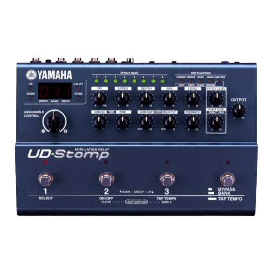
Page 4: Panel Layout
UD-Stomp PANEL LAYOUT Top Panel Controller Section Display & Main Section Footswitch Section Display & Main Section Up Button (UP) Down Button (DOWN) Utility Button (UTILITY) Store Button (STORE) Display... - Page 5 UD-Stomp Controller Section ASSIGNABLE CONTROL TAP Control EFFECT BAND 1-8 SPEED Control EDIT FUNCTION DEPTH Control Delay Time Control: Coarse (TIME COARSE) PAN Control Delay Time Control: Fine (TIME FINE) Delay Level Control (LEVEL) LOW CUT FILTER Control EFFECT LEVEL Control...
-
Page 6: Circuit Board Layout
UD-Stomp Rear Panel Power Switch (STAND-BY ON/OFF) Expression Pedal Jack (EXP. PEDAL) Power Adaptor Jack (AC IN 12V 1A) Headphones Jack (PHONES) MIDI OUT Jack Output Jacks (OUTPUT R, L/MONO) MIDI IN Jack Input Level Switch (LOW/HIGH) DIGITAL OUT Jack... -
Page 7: Wiring
UD-Stomp WIRING Shield Sheet CN302 CN305 CN301 CN304 CN303 (V610850) CN307 CN306 CN310 CN309 CN308 (V611470) (V611460) (V611450) Note) When installing the DM circuit board, use care not to have the wire assembly caught by the bottom case. CN103 (V611480) -
Page 8: Block Diagram
UD-Stomp BLOCK DIAGRAM SW101 CN103 IC103 IC103 VR314 CN301 CN301 IC101 IC104 IC102 IC102 IC10, IC11 IC2, IC3 DOUT IC12 SW-R0~R3 AN0~AN3 , SELECT A , SELECT B PN-PB0~PB7 ( DM1/2-CN1 ) ( DM-CN3 ) ( PN1/2-CN304 ) ( PN1/2-CN302 ) - Page 9 UD-Stomp IC105 VR314 CN103 CN301 CN301 IC105 IC106 TRS BALANCE OUT IC106 TRS BALANCE OUT 15 , 17 LED-FOOT SW-010 RXDO , TXDO LED-REV SW-100 LED-MOD SW-LINE SW-001 ( DM-CN2 ) ( PN1/2-CN303 ) IC112, IC113, IC114 KEC-54241...
-
Page 10: Disassembly Procedure
UD-Stomp DISASSEMBLY PROCEDURE Bottom Case (Manhour requirement: 1 min.) Remove the six (6) screws marked [30]. The bottom case can then be removed. (Fig. 1) Bottom [30] [30] [30]:Bind Head Tapping Screw-B 3.0x8 MFZN2BL (EP600190) Fig.1 Battery VS246400 DM Circuit Board VS246300(Battery holder for VS246400) (Manhour requirement: 6 min.) - Page 11 UD-Stomp Topcover [T70] [T110B] [T70]:Washer 9.0 MFZN2Y (ET800150) [T110]:Bind Head Tapping Screw-B 3.0x8 MFZN2BL (EP600190) Fig.2 PN1/2 Circuit Boards PN 2/2 Circuit Board (Manhour requirement: 10 min.) (Manhour requirement: 13 min.) 4-1. Remove the bottom case. (See Procedure 1.) 3-1.
- Page 12 UD-Stomp Heat Sink (Manhour requirement: 8 min.) 5-3. Remove the two (2) screws marked [A-a] from the 5-1. Remove the bottom case. (See Procedure 1.) soldered face of the DM circuit board and the three 5-2. Remove the DM circuit board. (See Procedure 2.) (3) screws marked [A-b] from IC112, IC113 and IC114.
-
Page 13: Lsi Pin Description
UD-Stomp LSI PIN DESCRIPTION HD6413002FP16 (XQ375A00) CPU DM: IC12 NAME FUNCTION NAME FUNCTION Port A Port A Power supply Address bus Port B Ground P60//WAIT PB6//DREQ0 P61//BREQ Port 6 PB7//DREQ1 /RESO Reset P62//BACK Ground Ø Øout, Ø=FAI P90/TXD0 /STBY Stand-by mode signal... - Page 14 UD-Stomp YSS910-S (XV988A00) DSP6 (Digital Signal Processor) DM: IC8 NAME FUNCTION NAME FUNCTION Power supply (3.3 V) Ground Ground DB13 System master clock input (60 MHz or 30 MHz) DB14 System master clock output (High or 30 MHz) DB15 Vdd5...
- Page 15 UD-Stomp YM3437C-F (XM530A00) DIT2 (Digital Format Interface Transmitter) DM: IC17 NAME FUNCTION NAME FUNCTION Ground MUTE Mute MCLK Master clock input Validity flag DIN/BCLK/WCLK format select C,U bit clock input/C bit data input DM1,DM0=0,0 DSP,LDSP (64 bit,LSB first) C,U bit data input/U bit data input...
-
Page 16: Ic Block Diagram
UD-Stomp IC BLOCK DIAGRAM MB3790PF(XR967A00) DM: IC4 ASSP 0.5Ω 100Ω CONTROL N.C. CONTROL 590kΩ Reference 2.65V N.C. BAT1 Voltage ALARM1 1.24V Power Supply 500Ω Circuit 3µA 2.37V ALARM2 SENSE BAT2 SENSE ALARM1 ALARM1 RESET RESET 240kΩ V th:3V RESET RESET V th:1.5V... - Page 17 UD-Stomp 74HC4052DT(XZ101A00) NJM072M(XC458A00) 74HC374DT(XZ102A00) PN: IC301~IC307 PN: IC308, IC309 DM: IC101 Multiplexer OP AMP D-FF +DC Voltage Output A Supply – + Inverting Output B Input A – Non-Inverting Inverting D CK Input B Input A –DC Voltage Non-Inverting –V...
-
Page 18: Circuit Boards
UD-Stomp CIRCUIT BOARDS DM Circuit Board INPUT L/MONO HIGH CN103: to PN1/2-CN301 to PN1 Battery VS246400 VS246300(Battery holder for VS246400) Battery • Notice for back-up battery removal Push against the holder hook, then the battery will pop up. • Druk tegen de houder, de batterij springt dan naar voren. - Page 19 UD-Stomp STANDBY AC IN ON OFF 12V 1A~ to PN1/2-CN302 to PN1/2-CN303 to PN1/2-CN304 Component side CNA-V838990...
- Page 20 UD-Stomp DM Circuit Board...
- Page 21 UD-Stomp Pattern side...
- Page 22 UD-Stomp PN 1/2 Circuit Board to PN2/2-CN306 to DM-CN3 PN 2/2 Circuit Board LD302, LD303, LD304 and LD305 installation SW301~SW317 installation Cathode side: Anode Red mark PN: CNA-V838980...
- Page 23 UD-Stomp to DM-CN3 to DM-CN2 to DM-CN1 to DM-CN103 Component side Component side...
- Page 24 UD-Stomp PN 1/2 Circuit Board PN 2/2 Circuit Board...
- Page 25 UD-Stomp Pattern side to PN1/2-CN305 Pattern side...
-
Page 26: Test Program
UD-Stomp TEST PROGRAM A. CONNECTION OF TERMINALS SW Check • INPUT Monaural input (1) Using the UP and DOWN switches, select “1”. • OUT L/MONO Monaural output (RL 47KΩ) (This step can be skipped if “1” is already selected.) • OUT R Monaural output (RL 47KΩ) - Page 27 UD-Stomp FC7 Foot Controller Fig.2 Battery check (1) Using the UP and DOWN switches, select “3”. SRAM Check (This step can be skipped if “3” has already been (1) Using the UP and DOWN switches, select “5”. selected.) (This step can be skipped if “5” is already selected.) (2) Press the STORE switch.
-
Page 28: Error Messages
UD-Stomp Table1 ITEM INPUT OUTPUT JK103(OUT L/MONO)+1.0dBm ± 3dB INPUT Sensitivity JK101(INPUT) -5dBm(1KHz) JK103(OUT L/MONO)+1.0dBm ± 3dB INPUT Sensitivity JK101(INPUT) -5dBm(10KHz) JK103(OUT L/MONO)+1.0dBm ± 3dB INPUT Sensitivity JK101(INPUT) -5dBm(100Hz) JK104(OUT R)-1.0dBm ± 3dB INPUT Sensitivity JK101(INPUT) -25dBm(100Hz) JK104(OUT R)-1.0dBm ± 3dB... -
Page 29: Midi Implementation Chart
UD-Stomp YAMAHA [ Modulation Delay] Date:14-Dec-2001 Model UD stomp MIDI Implementation Chart Version : 1.0 +----------------------------------------------------------------------+ Transmitted Recognized Remarks Function ... : :-------------------+----------------+----------------+----------------: :Basic Default : 1 - 16 : 1 - 16, off : memorized :Channel Changed : 1 - 16... -
Page 30: Parts List
PARTS LIST CONTENTS OVERALL ASSEMBLY ............. 2 ELECTRICAL PARTS ..............4 Notes : DESTINATION ABBREVIATIONS A : Australian model M : South African model B : British model O : Chinese model C : Canadian model Q : South-east Asia model D : German model T : Taiwan model E : European model... -
Page 31: Overall Assembly
UD-Stomp OVERALL ASSEMBLY T120 T110 T40 (1/2) T40 (2/2) T130 T160 T150 T140 T170 T110 T110 T100 T180 T110... - Page 32 UD-Stomp PART NO. DESCRIPTION REMARKS REF NO. RANK Overall Assembly (V839770) Top Cover Assembly (V839830) V 8 3 9 8 4 0 0 Bottom Case EP600190 Bind Head Tapping Screw-B 3.0X8 MFZN2BL V 3 6 9 4 1 0 0...
-
Page 33: Electrical Parts
UD-Stomp ELECTRICAL PARTS PART NO. DESCRIPTION REMARKS REF NO. RANK ELECTORICAL PARTS UD-STOMP V 8 3 8 9 9 0 0 Circuit Board (X2186B0) AAX33470 Circuit Board PN1/2 (V838980)(X2180B0) AAX33480 Circuit Board PN2/2 (V838980)(X2180B0) V 8 3 8 9 9 0 0... - Page 34 UD-Stomp PART NO. DESCRIPTION REMARKS REF NO. RANK C0138 UX061220 Ceramic Capacitor (Chip) 22P 50V J C0139 UR857100 Electrolytic Cap. 10.00 35.0V C0140 V 6 1 9 7 0 0 0 Electrolytic Cap.-BP 47.00 25.0V C0141 UX063100 Ceramic Capacitor (Chip)
- Page 35 UD-Stomp PART NO. DESCRIPTION REMARKS REF NO. RANK IC014 XZ109A00 74HC244DT BUFFER -016 XZ109A00 74HC244DT BUFFER IC017 XM530A00 YM3437C-F DIT2 IC018 XU965A00 UPC29M33T-E1 REGULATOR +3.3V IC101 XC458A00 NJM072M OP AMP IC102 XC011A00 NJM5532M OP AMP IC103 XC011A00 NJM5532M OP AMP...
- Page 36 UD-Stomp PART NO. DESCRIPTION REMARKS REF NO. RANK R0117 RG107100 Carbon Resistor (chip) 10K 0.1 F R0118 RG105470 Carbon Resistor (chip) 470 0.1 F R0119 RG106270 Carbon Resistor (chip) 2.7K 0.1 F R0120 RG006560 Carbon Resistor (chip) 5.6K 0.1 J...
- Page 37 UD-Stomp PART NO. DESCRIPTION REMARKS REF NO. RANK AAX33470 Circuit Board PN1/2 (V838980)(X2180B0) AAX33480 Circuit Board PN2/2 (V838980)(X2180B0) V 6 2 2 0 8 0 0 Spacer V 6 6 2 4 6 0 0 LED Holder LED3-1A Connector Assembly C&...
- Page 38 UD-Stomp PART NO. DESCRIPTION REMARKS REF NO. RANK VR311 V 5 2 6 4 8 0 0 Rotary Variable Resistor RK09L1140 10KB VR312 V 5 2 6 4 8 0 0 Rotary Variable Resistor RK09L1140 10KB LEVEL VR313 V 5 2 6 4 8 0 0...
- Page 39 UD-Stomp OVERALL CIRCUIT DIAGRAM 1/3 (DM) UD-Stomp Photo Coupler MIDI OUT MIDI IN ASSP SRAM 256K SRAM 256K ROM 8M BUFFER to P2.G3 to PN1/2-CN304 BUFFER BUFFER to PN1/2-CN303 from P2.K6 to PN1/2-CN302 to P2.K6 DSP6 DRAM 4M EXP.PEDAL DIGITAL...
- Page 40 UD-Stomp OVERALL CIRCUIT DIAGRAM 2/3 (DM) UD-Stomp OP AMP PHONSE OP AMP INPUT OPAMP OPAMP OPAMP OP AMP OUTPUT (L/MONO) ADC & DAC OPAMP OPAMP INVERTER OUTPUT OPAMP OP AMP REGULATOR +5V SHIFT D-FF REGISTER B. COUNTER INVERTER from P1.A6 to P1.A5, P1.G8...
- Page 41 UD-Stomp OVERALL CIRCUIT DIAGRAM 3/3 (PN 1/2 , PN 2/2) UD-Stomp D-FF D-FF 7 segment LED 3 figures D-FF D-FF D-FF D-FF to DM-CN103 to DM-CN1 to DM-CN2 TIME FILTER DIRECT DIRECT ASSIGNABLE CONTROL COARSE FINE LOW CUT HIGH CUT...