Advertisement
Quick Links
Download this manual
See also:
Instruction Manual
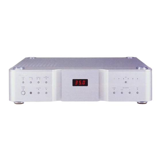
AX-M9000
SERVICE MANUAL
MONAURAL INTEGRATED AMPLIFIER
AX-M9000
Area Suffix
E
Continental Europe
GAIN CONTROL
EXT
PHASE
SPEAKER
PRESENCE
PROCESSOR
LINE
-180û
1
2
1
2
1
2
3
4
5
6
STANDBY/ON
SLEEP
EACH
MUTE
ATT
DOWN
UP
AX M9000
MONAURAL INTEGRATED AMPLIFIER
Contents
Safety precautions --------------------------------------------------------1-2
Disassembly method -----------------------------------------------------1-3
Adjustment method -------------------------------------------------------1-10
Description of major ICs -------------------------------------------------1-11~21
No.20933
COPYRIGHT
2001 VICTOR COMPANY OF JAPAN, LTD.
Apr.2001
Advertisement

Related Manuals for JVC AX-M9000


Summary of Contents for JVC AX-M9000
- Page 1 AX-M9000 SERVICE MANUAL MONAURAL INTEGRATED AMPLIFIER AX-M9000 Area Suffix Continental Europe GAIN CONTROL PHASE SPEAKER PRESENCE PROCESSOR LINE -180û STANDBY/ON SLEEP EACH MUTE DOWN AX M9000 MONAURAL INTEGRATED AMPLIFIER Contents Safety precautions --------------------------------------------------------1-2 Disassembly method -----------------------------------------------------1-3 Adjustment method -------------------------------------------------------1-10 Description of major ICs -------------------------------------------------1-11~21 No.20933...
- Page 2 AX-M9000 1. This design of this product contains special hardware and many circuits and components specially for safety purposes. For continued protection, no changes should be made to the original design unless authorized in writing by the manufacturer. Replacement parts must be identical to those used in the original circuits. Services should be performed by qualified personnel only.
- Page 3 AX-M9000 Disassembly method Metal cover Removing the metal cover (See Fig. 1) Remove the three screws A attaching the metal cover on the back of the body. Remove the four screws B attaching the metal cover on both sides of the body using a hexagon wrench.
- Page 4 AX-M9000 Removing the rear panel (See Fig.6 to 9) Prior to performing the following procedure, remove the metal cover and front panel assembly. Remove the four screws H attaching the rear panel on the back of the set. Remove the eight screws I attaching the rear panel on the upper part of the set.
- Page 5 AX-M9000 <Removing the front panel section> Removing the control switch board Front panel (right) Front panel (left) Sub-panel assembly 1 & 2 and display board assembly (See Fig.10 to 11) Prior to performing the following procedure, remove the metal cover and front panel assembly.
- Page 6 AX-M9000 Power AMP board TB402 TB401 CN453 CN402 CN401 TB403 TB404 Signal processing board CN301 Heat sink cover Fig.13 Removing the power AMP board assembly / heat sink (See Fig. 13 to 15) Prior to performing the following procedure, remove the metal cover, system control assembly and rear cover.
- Page 7 AX-M9000 Removing the current mode source Current mode source selector board assembly selector board assembly and rear terminal panel (See Fig. 16) Prior to performing the following procedure, remove the metal cover and the rear panel. Remove the six screws W attaching the RCA pins on the current mode source selector board assembly.
- Page 8 AX-M9000 Removing the core transformer for pre-AMP (See Fig. 19) Prior to performing the following procedure, remove the metal cover. Remove the two screws A attaching the power transformer for pre-AMP. Power transformer for pre-AMP Removing the transformer Fig.19 for power AMP (See Fig.
- Page 9 AX-M9000 Arrangement drawings for the clamp binding In order to secure the performance of the machine, refer to the following arrangement drawings when the lines are clamped. CLAMP Orange, Blue wire CN insertion Gray wire Red, Black wire CN insertion...
-
Page 10: Adjustment Method
AX-M9000 Adjustment method 1. List of measuring devices Measuring devices : Electronic voltmeter Oscilloscope Low-frequency transmitter (50Hz-20 kHz of transmitting frequency and output of 0 dBs at the 600 terminal) Distortion factor tester (with a built-in band path filter) 2. Adjustments and confirmation... - Page 11 AX-M9000 Description of major ICs BU2114F-X (IC542,543,544) : LED controller 1. Pin layout LATCH SOUT 2. Pin function Function Pin No. Symbol Serial data input terminal Shift lock of the shift register When this terminal is set at "L", the latch output will be secured,...
- Page 12 AX-M9000 MN101CP10A(IC521) : System controller 1.Pin layout 32 33 2. Pin function Pin No. Symbol Pin No. Symbol Pin function Pin function KY10 (DOWN) ROT1 Rotary input 1 Key input 10 KY11 (LINE) Line decoder C Key input 11 KY12 (MUTE)
- Page 13 AX-M9000 NJM2903M-XE(IC454) : Temperature detector 1. Pin layout A OUTPUT B OUTPUT A -INPUT A +INPUT B -INPUT B +INPUT (TOP VIEW) 2. Block diagram Q110 Q109 Q111 Q112 D103 D104 D101 D102 Q104 Q103 +INPUT Q101 Q102 Q108 -INPUT...
- Page 14 AX-M9000 NJM5532M-D-W(IC152,153) : Presence circuit amp 1. Pin layout A OUT A - IN B OUT A + IN B - IN B + IN 2. Block diagram +INPUT INPUT OUTPUT 1-14...
- Page 15 AX-M9000 OPA134PA(IC108, 201, 301) : OP Amp. Pin layout Offset Trim Offset Trim - In + In Output 8-Pin DIP, SO-8 TC74HC04AF(IC264) : Data line buffer Pin layout (TOP VIEW) 1-15...
- Page 16 AX-M9000 TC74HC238AF-X(IC525) : Line recorder 1. Pin layout (TOP VIEW) 2. Truth table INPUTS OUTPUTS ENABLE SELECT SELECTED OUTPUT Y1 Y2 Y3 Y4 Y5 Y6 Y7 G1 G2A G2B C NONE NONE NONE X : Don't Care 3. Block diagram...
- Page 17 AX-M9000 TC74HC27AF-W(IC531) : Noa gate 1. Pin layout 2. Truth table X : Don't Care (TOP VIEW) TC74VHC08F-X(IC281) : Dataline buffer 1. Terminal layout 2. Truth table X : Don't Care (TOP VIEW) 1-17...
- Page 18 AX-M9000 TC74HC373HF-X(IC522, IC523, IC524) : Shift register for relay control 2. Truth table 1. Pin layout OUTPUTS INPUTS X : Don't Care Z : High impedance Qn: The Q output level immediately before the LE becomes to "L". (TOP VIEW) 3.
- Page 19 AX-M9000 TC74VHC123AF-X(IC532) : Monostable multivibrator 1. Pin layout 1Rx/Cx 1CLR 2CLR 2Rx/Cx (TOP VIEW) 2. Block diagram Vref Vref CK Q 3. Timing diagram refH RX/CX refL w OUT w OUT w OUT+ 1-19...
- Page 20 AX-M9000 UPC1237HA (IC453) : Protection IC 1. Pin layout 2. Block diagram Q12 Q14 1-20...
- Page 21 AX-M9000 VC5022-2(IC302) : Advanced super A Block diagram 1.6k 1.6k 1.6k 1-21...
-
Page 22: Block Diagram
AX-M9000 Block diagram... - Page 23 AX-M9000 Standard schematic diagrams System control section ALL_L PRO_L ABS_L PWR_L PRE1_L PRE2_L Q526 DTA114YKA-X HPS_L R594 R595 CN602 QGA2001C1-12 IC511 GP1U561 Q504 DTD123TK-X Q505 C541 DTD123TK-X IC522 HPS_L TC74HC373AF-X Q506 CN502 DTD123TK-X PRE1_L PRE1 CN603 Q507 CN511 QGA2001C1-10 ATT_L...
- Page 24 AX-M9000 Main section (Premain AMP., Power supply) R127 C110 R129 R132 C109 22/25 R125 RY141 RY108 3.9k D301 R313 HZ3ALL-T2 R305 D311 IC108 R315 HZ3ALL-T2 R131 OPA134PA 100k R130 R143 R383 D381 Q311 3.9k C129 C600 HZ16-3L-T2 2SA1546/K/ R317 150P...
-
Page 25: Printed Circuit Boards
AX-M9000 Printed circuit boards Power switch board Power AMP. board (Reverse side) TB12 TB22 TB11 TB21 TB31 TB32 Current mode source selector board J103 J105 J106 J107 J104 J108 Power amp. sub board 2 Power amp. sub board 1 Q329... - Page 26 AX-M9000 Power AMP. board (Forward side) Power switch board TB12 TB22 TB11 TB21 TB31 TB32 Current mode source selector board Power amp. sub board 1 Power amp. sub board 2 J108 J107 J106 J105 J104 J103 Q329 Q327 Q328 Q330...
- Page 27 AX-M9000 Signal control board (Reverse side) CN251 CN252 R501 C501 R502 WR102 R270 D502 R282 D501 C502 R271 Q261 R272 R506 C506 R273 R509 R283 WR103 IC263 WR104 D506 Q281 C509 C505 D509 K257 R281 C252 K256 K255 D505 R279...
- Page 28 AX-M9000 Signal control board (Forward side) CN252 CN251 D282 D501 D502 C281 D506 D505 Q281 WR104 D509 WR103 C258 C257 C150 CP252 CP251 D507 RY141 CP258 CP257 D508 R257 R125 R258 C254 C253 R127 R143 C141 R254 R255 L101 R253...