Table of Contents
Advertisement
Quick Links
Advertisement
Table of Contents

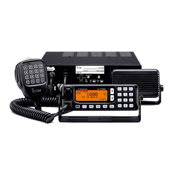
Related Manuals for Icom IC-F7000


Summary of Contents for Icom IC-F7000
- Page 1 Nov. 2007 SERVICE MANUAL ADDENDUM CONTENTS PARTS LIST ....... . 1 BOARD LAYOUTS .
-
Page 2: Parts List
Nov. 2007 PARTS LIST [MAIN UNIT] [MAIN UNIT] ORDER ORDER DESCRIPTION DESCRIPTION LOCATION LOCATION 1110004080 S.IC uPC2709T-E3 191.6/111.2 D114 1750000581 S.DIO 1SV307 (TPH3,F) 181.2/71.6 IC101 1130013860 S.IC IS62C1024AL-35TL1u 111.3/50.6 D115 1750000581 S.DIO 1SV307 (TPH3,F) 189.2/71.3 IC301 1110004080 S.IC uPC2709T-E3 133.1/22 D116 1750000581 S.DIO 1SV307 (TPH3,F) - Page 3 [MAIN UNIT] [MAIN UNIT] ORDER ORDER DESCRIPTION DESCRIPTION LOCATION LOCATION L128 6180003410 COL SP0406-2R2K-6 L2052 6200002041 S.COL NLV25T-101J 46/12.6 L129 6180003370 COL SP0406-R68K-6Z L2053 6200002041 S.COL NLV25T-101J 44.6/9.5 L130 6180003360 COL SP0406-R47K-6Z L2054 6200003950 S.COL HF50ACC 322513-T 51.6/12.6 L131 6180003340 COL SP0406-R33K-6Z L2055 6180003620 COL...
- Page 4 [MAIN UNIT] [MAIN UNIT] ORDER ORDER DESCRIPTION DESCRIPTION LOCATION LOCATION R401 7030003440 S.RES ERJ3GEYJ 102 V (1 k) 139.3/60.4 R1203 7030003760 S.RES ERJ3GEYJ 474 V (470 k) 67.4/7.3 R404 7030005691 S.RES ERA3YED 123V (12 k) 134.6/80.8 R1204 7030003860 S.RES ERJ3GE JPW V 70.2/30.3 R405 7030003490 S.RES ERJ3GEYJ 272 V (2.7 k)
- Page 5 [MAIN UNIT] [MAIN UNIT] ORDER ORDER DESCRIPTION DESCRIPTION LOCATION LOCATION R1721 7030003400 S.RES ERJ3GEYJ 471 V (470) 31.3/70.1 R3605 7030003580 S.RES ERJ3GEYJ 153 V (15 k) 104.6/14.8 R1722 7030003440 S.RES ERJ3GEYJ 102 V (1 k) 33.9/68.8 R3606 7030003640 S.RES ERJ3GEYJ 473 V (47 k) 107.1/11.5 R1723 7030003440 S.RES ERJ3GEYJ 102 V (1 k)
- Page 6 [MAIN UNIT] [MAIN UNIT] ORDER ORDER DESCRIPTION DESCRIPTION LOCATION LOCATION C125 4030007050 S.CER C1608 CH 1H 220J-T 210.2/89.5 C230 4030007170 S.CER C1608 CH 1H 221J-T 178.2/34.7 C126 4030007050 S.CER C1608 CH 1H 220J-T 214.6/86.1 C231 4030006880 S.CER C1608 JB 1H 472K-T 182.1/23.7 C127 4030008920 S.CER C1608 JB 1H 473K-T...
- Page 7 [MAIN UNIT] [MAIN UNIT] ORDER ORDER DESCRIPTION DESCRIPTION LOCATION LOCATION C803 4030011600 S.CER C1608 JB 1E 104K-T 110.5/82.4 C1710 4030014300 S.CER C1608 JB 1E 563K-T 19.8/53.3 C805 4030006880 S.CER C1608 JB 1H 472K-T 107.2/79.6 C1711 4030014300 S.CER C1608 JB 1E 563K-T 24.2/52.7 C806 4510008520 S.ELE...
- Page 8 Nov. 2007 BOARD LAYOUTS • MAIN UNIT V100 V105 V110 V115 (TOP VIEW) C1557 C1606 IC1601 C1559 R1556 L1551 IC1602 C1561 C1563 L1601 R1054 R1701 C1609 R1055 C1551 C1063 C1555 R1110 C1051 R1051 C1011 C1706 C1713 R1711 C1656 R1660 D1552 C1062 R1007 D1551...
- Page 9 • MAIN UNIT V115 V110 V105 V100 (BOTTOM VIEW) S-14012HH-P2-q Printed in Japan © 2003−2007 Icom Inc.
- Page 10 Nov. 2007 VOLTAGE DIAGRAM 100U 1SV307 0.0022 0.0022 0.0012 1SV307 TMP-J01X-V6 UPC2709T 0.18U 0.27U R6 1 R122 22 P 2SC4213 IC 1 82 P R127 L150 L154 100U 100U R204 C183 D122 C127 L101 L118 0.047 MMBFU310 C176 1SV307 MP201 Q201 3.9U 4.7U...
- Page 11 TMP-J01X-V6 J301 R310 R312 R320 R323 M2Lo MP40 1 EARTH SPRING(D) UPC2709T R315 C304 C307 L308 L504 0 .12U 1SV307 100U IC301 Q203 CFWS455HT 3SK131 L401 3SK131 LS-450 D133 LS-483A FI401 LS-542 C508 C51 8 FI402 LS-54 2 IC501 L210 LS-542 0.0047 L403...
- Page 12 HF TRANSCEIVER S-14012HZ-C1-q Jul. 2007...
- Page 13 8. READ the instructions of test equipment throughly before connecting a test equipment to the transceiver. Icom, Icom Inc. and logo are registered trademarks of Icom Incorporated (Japan) in the United States, the United Kingdom, Germany, France, Spain, Russia and/or other countries.
-
Page 14: Table Of Contents
IC-F7000 ........ -
Page 15: Ic-F7000
SECTION 1 SPECIFICATIONS • IC-F7000 M General Transceiver • Frequency coverage : • Output power (Unit: MHz) Receive 0.5–29.9999 1.6–27.9999 MHz 100/50/10 W p-p [AUS] Transmit 1.6–5.4999 5.73–5.9999 1.6–3.9999 MHz 125/50/10 W p-p [OTH] 6.7–8.0999 10.0–11.1999 4.0–27.9999 MHz 100/50/10 W p-p [OTH] 13.4–14.9999... - Page 16 SECTION 2 INSIDE VIEWS • RC-26 (IC8201: HD64F2134AF20) (IC8201: HD64F2134AF20) Reset IC Reset IC (IC8202: S-80942CNMC-G9C) (IC8202: S-80942CNMC-G9C) +8V regulator +8V regulator (IC8310: TA78L08F) (IC8310: TA78L08F) +10V regulator +10V regulator (IC8301: AN8009M) (IC8301: AN8009M) +5V regulator +5V regulator (IC8290: TA7805F) (IC8290: TA7805F) CONNECT BOARD CONNECT BOARD...
- Page 17 • IC-F7000 TX 1st mixer TX 1st mixer (Q702,Q703: 3SK131) (Q702,Q703: 3SK131) YGR amplifier YGR amplifier (IC1: μPC2709T) (IC1: μPC2709T) RF 1st mixer RF 1st mixer (Q201-Q204: MBU310×4) 1st IF amplifier 1st IF amplifier (Q203: 3SK131) (Q203: 3SK131) 2nd mixer...
- Page 18 SECTION 3 EXT. REFERENCE SIGNAL SOURCE ‘ ‘ IN CASE OF USING EXTERNAL REFERENCE SIGNAL the PLL unit (bottom side) as below when using external reference. NEED TO MODIFY q Remove R5251 from the PLL unit. w Solder disconnect points (CP5041) on the PLL unit. R5251 CP5041 3 - 1...
- Page 19 Solder R5251 to the original position, or solder disconnect points (CP5251) on the PLL unit. CP5251 CP5041 ‘ ‘ CONNECTION Connect the external reference oscillator to the IC-F7000 as below. IC-F7000 front panel External reference Frequency : 32 MHz [REF IN] Level : 2.0–8.0 V...
-
Page 20: Receiver Circuits
SECTION 4 CIRCUIT DESCRIPTION 4-1 RECEIVER CIRCUITS 4-1-2 1ST MIXER AND IF CIRCUITS (MAIN UNIT) 4-1-1 RF FILTER CIRCUIT (PLL AND MAIN UNITS) The 1st mixer circuit converts the received signals into a Received signals from the antenna connector are applied fixed frequency, 64.445 kHz 1st IF signal using PLL output to the transmit/receive switching and protection relay (PLL frequency. -
Page 21: Main Unit (1)
4-1-5 DSP RECEIVER CIRCUIT (MAIN AND DSP The 3rd IF signal from the CODEC IC (IC9501) is detected UNITS) at the AGC detector section in the DSP IC (IC9301). The DSP (Digital Signal Processor) circuit enables digital The output signal from the DSP IC is level-shifted at the IF filter, digital noise reduction, digital PSN (Pulse Shift level converter (IC9101) and applied to the D/A converter Network), phase demodulation, digital automatic notch, and... -
Page 22: Transmitter Circuits
When the speech compressor function is ON, the level- 4-2 TRANSMITTER CIRCUITS shifted signal from the CODEC IC (IC9501) is applied to 4-2-1 MICROPHONE AMPLIFIER CIRCUIT the DSP IC (IC9301) and compressed at the DSP IC to (RC-26, MAIN AND DSP UNITS) obtain an average audio level. - Page 23 4-2-5 RF CIRCUIT (MAIN, PA, PLL UNITS AND • 2.5–3.49999 MHz signals The signals are applied to the relay (FILTER unit; RL7061). DRIVER BOARD) The signals pass through the low-pass filter (FILTER unit; The RF circuit amplifies operating (transmitting) frequency L7067, L7068, C7072, C7073, C7077–C7083), and are to obtain 100 W (125 W: 1.6–4 MHz for [OTH]) of RF then applied to the RL7062 which is controlled by the band...
-
Page 24: Pll Circuits
4-2-6 ALC CIRCUIT (PLL AND MAIN UNITS) 4-2-8 RF METER CIRCUIT (MAIN UNIT) The ALC (Automatic Level Control) circuit controls the The output of ALC amplifier (IC1201, pin 14) is applied to gain of IF amplifiers in order for the transceiver to output a the CPU (IC3303, pin 97) as “RFML”... - Page 25 4-3-3 2ND LO AND REFERENCE OSCILLATOR AF amplifier (IC8280) via the “MIC” signal. The signals are CIRCUITS (PLL UNIT) applied to the IC-F7000’s main unit through the J2501, pin The reference oscillator (X5251) generates a 32.0 MHz 1 via the “FMOD” line.
-
Page 26: Power Supply Circuits
4-5 POWER SUPPLY CIRCUITS 4-5-4 MAIN UNIT VOLTAGE LINE 4-5-1 PA UNIT VOLTAGE LINE LINE DESCRIPTION LINE DESCRIPTION S13V The voltage from the PA unit via the J1901. HV13 The voltage from an external power supply. Receive 13 V converted from the S13V line and R13V regulated by the R13 regulator circuit (Q1505). -
Page 27: Port Allocations
4-6 PORT ALLOCATIONS MAIN CPU (MAIN UNIT; IC3303)–continued 4-6-1 MAIN CPU (MAIN UNIT; IC3303) Port Port Description Description number name number name Outputs T8 regulator circuit (MAIN Outputs serial clock signal for the unit; Q1501) control signal. EEPROM (IC3301, pin 6). Outputs R8 and R13V regulator Input port for the SEND signal from ASEN... - Page 28 4-6-4 OUTPUT EXPANDER IC FOR BANDPASS 4-6-6 D/A CONVERTER IC (MAIN UNIT; IC3606) FILTERS (MAIN UNIT; IC3604) Port Description Port number name Description number name Outputs transmit power control Outputs 0.5–1.999999 MHz bandpass signal. The signal is applied to the POCV filter control signal.
- Page 29 4-6-7 FRONT CPU PORT ALLOCATIONS (RC-26, DISPLAY BOARD; IC8201) Port Port Description Description name number number name Input port for the [7] switch. 15–17 Low: [7] switch is pushed. Outputs LCD drive signals. Input port for the [6] switch. Low: [6] switch is pushed. Input port for the [CALL] switch.
- Page 30 SECTION 5 ADJUSTMENT PROCEDURE 5-1 PREPARATION When adjusting the contents on page 5-9, a JIG CABLE (see illustration as below) is required. Some adjustments must be performed on the “ADJUSTMENT MODE”. Entering the “ADJUSTMENT MODE”, refer to the next page in detail. M REQUIRED TEST EQUIPMENT EQUIPMENT GRADE AND RANGE...
- Page 31 M ENTERING THE ADJUSTMENT MODE q Turn the power OFF. w Push and hold the HM-146’s [CALL] and RC-26’s [EMG] switches, then turn the power ON. [POWER] [EMG] [CALL] Connect to [MIC] connector. M OPERATING ON THE ADJUSTMENT MODE • Enter the TX adjustment from the MAIN menu. : Push the RC-26 [1] button •...
-
Page 32: Pll Unit Adjustment
5-2 PLL UNIT ADJUSTMENT MEASUREMENT ADJUSTMENT ADJUSTMENT ADJUSTMENT CONDITIONS VALUE UNIT LOCATION UNIT ADJUST LPL LOCK • Operating frequency : 0.5000 MHz Connect a digital multi 1.0 V C5305 VOLTAGE • Mode : J3E meter or oscilloscope • Receiving to the check point CP5301. - Page 33 • IC-F7000 BOTTOM VIEW PLL unit • PLL UNIT TOP VIEW C5521 HPL lock voltage adjustment R5255 CP5402 L5203 HPL lock voltage ckeck point L5204 Reference frequency adjustment P5201 Reference frequency ckeck point CP5302 LPL lock voltage ckeck point L5305...
- Page 34 5-3 PA AND FILTER UNITS ADJUSTMENT MEASUREMENT ADJUSTMENT ADJUSTMENT ADJUSTMENT CONDITIONS VALUE UNIT LOCATION UNIT ADJUST IDLING • Operating frequency : 12.2350 MHz Rear Connect an ammeter 2.0 A R6304 CURRENT • Mode : J3E panel (10 A) between an ( For drive •...
- Page 35 (For final transistors) R6304 Idling current adjustment (For drive FETs) • PLL UNIT BOTTOM VIEW CP7331 (REF line) SWR detector check point CP7332 (FOR line) Connect to ground C7275 SWR detector adjustment • IC-F7000 BOTTOM VIEW FILTER unit 5 - 6...
-
Page 36: Receiver Adjustments
5-4 RECEIVER ADJUSTMENTS ”TOTAL GAIN”, “S-METER” and “DSC PEAK” adjustments must be performed at “ADJUSTMENT MODE”. MEASUREMENT ADJUSTMENT ADJUSTMENT ADJUSTMENT CONDITIONS VALUE UNIT LOCATION UNIT ADJUST NOISE NULL • Operating frequency : 0.5 MHz Front C o n n e c t Minimum output MAIN R217,... -
Page 37: Main Unit (2)
• MAIN UNIT TOP VIEW MAIN unit L401 L403 Preset to max. counter clockwise L801 L404 L405 R217 R218 Noise null point adjustment L207 L208 L211 L210 Noise null point adjustment L209 Preset to top edge of its chassis L209 PRESETTING Set to same height here. -
Page 38: Transmitter Adjustments
5-5 TRANSMITTER ADJUSTMENTS The following adjustments must be performed at “ADJUSTMENT MODE” after “SWR DETECTOR” and “RECEIVER” ADJUSTMENTS in the SECTION 5-3 and 5-4. MEASUREMENT ADJUSTMENT ADJUSTMENT ADJUSTMENT CONDITIONS VALUE UNIT LOCATION UNIT ADJUST TRANSMIT Rear Connect an RF power Maximum MAIN L706... - Page 39 TRANSMITTER ADJUSTMENTS–Continued MEASUREMENT ADJUSTMENT ADJUSTMENT ADJUSTMENT CONDITIONS VALUE UNIT LOCATION UNIT ADJUST 1 • Operating frequency : 13.810 MHz Rear 24.0 A [AUS] R6516 IC-APC Connect an ammeter • Mode : J3E panel 28.0 A [OTH] (50 A) between an •...
-
Page 40: Parts List
SECTION 6 PARTS LIST [MAIN UNIT] [MAIN UNIT] ORDER ORDER DESCRIPTION DESCRIPTION LOCATION LOCATION 1110004080 S.IC uPC2709T-E3 191.6/111.2 D114 1750000581 S.DIO 1SV307 (TPH3,F) 181.2/71.6 IC101 1130013860 S.IC IS62C1024AL-35TL1 <TOMO> 111.3/50.6 D115 1750000581 S.DIO 1SV307 (TPH3,F) 189.2/71.3 IC301 1110004080 S.IC uPC2709T-E3 133.1/22 D116 1750000581 S.DIO... - Page 41 [MAIN UNIT] [MAIN UNIT] ORDER ORDER DESCRIPTION DESCRIPTION LOCATION LOCATION L128 6180003410 COL SP0406-2R2K-6 L2052 6200002041 S.COL NLV25T-101J 46/12.6 L129 6180003370 COL SP0406-R68K-6Z L2053 6200002041 S.COL NLV25T-101J 44.6/9.5 L130 6180003360 COL SP0406-R47K-6Z L2054 6200003950 S.COL HF50ACC 322513-T 51.6/12.6 L131 6180003340 COL SP0406-R33K-6Z L2055 6180003620 COL...
- Page 42 [MAIN UNIT] [MAIN UNIT] ORDER ORDER DESCRIPTION DESCRIPTION LOCATION LOCATION R405 7030003490 S.RES ERJ3GEYJ 272 V (2.7 k) 132.7/80 R1205 7030005871 S.RES ERA3YKD 104V (100 k) 64.7/22.5 R406 7030003760 S.RES ERJ3GEYJ 474 V (470 k) 132.9/83.8 R1206 7030003760 S.RES ERJ3GEYJ 474 V (470 k) 64.7/23.8 R407 7030003320 S.RES ERJ3GEYJ 101 V (100)
- Page 43 [MAIN UNIT] [MAIN UNIT] ORDER ORDER DESCRIPTION DESCRIPTION LOCATION LOCATION R1723 7030003440 S.RES ERJ3GEYJ 102 V (1 k) 34.7/67 R3606 7030003640 S.RES ERJ3GEYJ 473 V (47 k) 107.1/11.5 R1724 7030009591 S.RES ERA3YED 472V (4.7 k) 118/4.5 R3608 7030003640 S.RES ERJ3GEYJ 473 V (47 k) 89.5/29.8 R1801 7030003500 S.RES ERJ3GEYJ 332 V (3.3 k)
- Page 44 [MAIN UNIT] [MAIN UNIT] ORDER ORDER DESCRIPTION DESCRIPTION LOCATION LOCATION C126 4030007050 S.CER C1608 CH 1H 220J-T 214.6/86.1 C231 4030006880 S.CER C1608 JB 1H 472K-T 182.1/23.7 C127 4030008920 S.CER C1608 JB 1H 473K-T 150.7/80.4 C232 4030006880 S.CER C1608 JB 1H 472K-T 173.1/30 C128 4030017810 S.CER C1608 CH 1H 102J-T...
- Page 45 [MAIN UNIT] [MAIN UNIT] ORDER ORDER DESCRIPTION DESCRIPTION LOCATION LOCATION C805 4030006880 S.CER C1608 JB 1H 472K-T 107.2/79.6 C1711 4030014300 S.CER C1608 JB 1E 563K-T 24.2/52.7 C806 4510008520 S.ELE EEE1CA470SP 117.1/89.2 C1713 4510008540 S.ELE EEE1CA100SR 16.7/58.5 C901 4030011600 S.CER C1608 JB 1E 104K-T 33.6/73.5 C1714 4510008540 S.ELE...
- Page 46 [PLL UNIT] [PLL UNIT] ORDER ORDER DESCRIPTION DESCRIPTION LOCATION LOCATION IC5001 1180001071 S.IC TA7805F (TE16L,Q) 99.8/20.2 L7096 6140002340 COL LR-263 (T68-2) [OTH], [EXP] only IC5031 1180001251 S.IC TA7808F (TE16L,Q) 90.7/20 L7097 6140002260 COL LR-238 (T68-2) [OTH], [EXP] only IC5081 1120002921 S.IC ADM202EARNZ 68.6/10.1 L7121...
- Page 47 [PLL UNIT] [PLL UNIT] ORDER ORDER DESCRIPTION DESCRIPTION LOCATION LOCATION R5147 7030003860 S.RES ERJ3GE JPW V 154.2/79 R7357 7030006060 S.RES ERJ12YJ100U (10) 53.6/47.4 R5148 7030008240 S.RES ERJ12Y0R00U 140.3/91 R7358 7030006060 S.RES ERJ12YJ100U (10) 53.7/43.1 R5203 7030003320 S.RES ERJ3GEYJ 101 V (100) 171.6/49.2 R5204 7030003600 S.RES ERJ3GEYJ 223 V (22 k)
- Page 48 [PLL UNIT] [PLL UNIT] ORDER ORDER DESCRIPTION DESCRIPTION LOCATION LOCATION C5351 4030006880 S.CER C1608 JB 1H 472K-T 183.2/60.2 C7125 4030011730 S.CER GRM31M2C2H101JV01L 70.5/87.3 C5352 4030006880 S.CER C1608 JB 1H 472K-T 174/56.4 C7126 4030014460 S.CER GRM31M2C2H820JV01L 81.4/82.3 C5353 4030006880 S.CER C1608 JB 1H 472K-T 182/56.6 C7127 4030011730 S.CER GRM31M2C2H101JV01L...
-
Page 49: Pa Unit
[PA UNIT] [PA UNIT] ORDER ORDER DESCRIPTION DESCRIPTION LOCATION LOCATION IC6501 1110002700 S.IC NJM2904M-TE1-#FMZB 113.7/15.8 R6512 7030003680 S.RES ERJ3GEYJ 104 V (100 k) 108.9/18.4 IC6601 1180001251 S.IC TA7808F (TE16L,Q) 171.5/19.8 R6513 7030003740 S.RES ERJ3GEYJ 334 V (330 k) 109/14.7 R6514 7030003680 S.RES ERJ3GEYJ 104 V (100 k) 106.8/18.4 R6515... -
Page 50: Driver Board
[PA UNIT] [DSP UNIT] ORDER ORDER DESCRIPTION DESCRIPTION LOCATION J6412 6510021391 CNR IMSA-9230B-1-03Z024-PT1 IC9001 1130010540 S.IC SN74AHC74PWR J6501 6510018961 S.CNR B2B-PH-SM4-TB (LF) (SN) 64.9/7.7 IC9003 1130010540 S.IC SN74AHC74PWR J6701 6510021721 S.CNR 30FLT-SM2-TB (LF) (SN) 104.2/80 IC9004 1130010540 S.IC SN74AHC74PWR J6702 6510007020 CNR TMP-J01X-V6 IC9005... -
Page 51: Dsp Unit
[DSP UNIT] [DSP UNIT] ORDER ORDER DESCRIPTION DESCRIPTION R9325 7030003560 S.RES ERJ3GEYJ 103 V (10 k) C9314 4030006880 S.CER C1608 JB 1H 472K-T R9326 7030003560 S.RES ERJ3GEYJ 103 V (10 k) C9315 4030011600 S.CER C1608 JB 1E 104K-T R9327 7030003560 S.RES ERJ3GEYJ 103 V (10 k) C9316 4030006880 S.CER C1608 JB 1H 472K-T R9328... -
Page 52: Front Unit
• [FRONT UNIT] ORDER DESCRIPTION ORDER DESCRIPTION R8240 7030003440 S.RESISTOR ERJ3GEYJ 102 V (1 kΩ) R8241 7030003800 S.RESISTOR ERJ3GEYJ 105 V (1 MΩ) W8001 8900009230 CABLE OPC-908 (P=1 N=10 L=60) ERJ3GEYJ 471 V (470 Ω) R8242 7030003400 S.RESISTOR W8002 8900012650 CABLE OPC-1272 TYX4003-210100 R8244... -
Page 53: Connect Board
[DISPLAY BOARD] [REAR BOARD] ORDER ORDER DESCRIPTION DESCRIPTION ERJ1TYJ 330U (33 Ω) C8311 4030011600 S.CERAMIC C1608 JB 1E 104K-T R8801 7030010540 S.RESISTOR ERJ1TYJ 330U (33 Ω) C8312 4030011600 S.CERAMIC C1608 JB 1E 104K-T R8802 7030010540 S.RESISTOR ERJ1TYJ 330U (33 Ω) C8313 4510004640 S.ELECTROLYTIC ECEV1CA470SP... -
Page 54: Driver Unit
SECTION 7 MECHANICAL PARTS • IC-F7000 [DRIVER UNIT] ORDER [CHASSIS PARTS] DESCRIPTION QTY. ORDER DESCRIPTION QTY. MP6851* 8410002480 2429 PA HEATSINK J4501 6510000370 MR-DS [PA UNIT] P4501 6510003240 TMP-P01X-A1 P4520 6510003240 TMP-P01X-A1 ORDER DESCRIPTION QTY. P4521 6510003240 TMP-P01X-A1 W4501 8900012620 OPC-1270... -
Page 55: Display Unit
• RC-26 [DISPLAY UNIT] ORDER DESCRIPTION QTY. J8201* 6510021261 B9B-ZR-SM4-TF (LF) (SN) J8202* 6510022621 10FMN-BMTTR-A-TBT (LF) (SN) J8205* 6510022541 20FMN-BMTTR-A-TBT (LF) (SN) J8701 6450001470 95003-2881 J8702* 6510022621 10FMN-BMTTR-A-TBT (LF) (SN) S8201 2250000480 EVE HE1 F25 24B [FRONT UNIT] ORDER DESCRIPTION QTY. -
Page 56: Pll Unit (1)
J5041 (P) MP4512 (C) MP8102 (R) MP1451 (M) J5081 (P) MP8104 (R) W4501 (C) (R): RC-26 MP8105 (R) J5051 (P) (F): IC-F7000 MP5701 (P) MP4509 (C) MP5103 (P) J5091 (P) EP1451 (M) MP5501 (P) J5041 (P) MP4501 (C) J5081 (P) - Page 57 SECTION 8 SEMICONDUCTOR INFORMATION • TRANSISTERS AND FETs • DIODES 2SA1037AK S 2SA1586 GR 2SB1201 S 2SC4081 T106 R 2SC4116 BL 1SS301 1SS322 1SS355 1SS375-TL 1SV307 (Symbol: FS) (Symbol: SG) (Symbol: B1201) (Symbol: BR) (Symbol: LL) (Symbol: B3) (Symbol: A9) (Symbol: A) (Symbol: FH) (Symbol: TX)
- Page 58 SECTION 9 BOARD LAYOUTS W7321 to MAIN unit J51 • PLL UNIT V10 V15 V20 V25 V30 V35 V40 V45 V50 V55 V60 V65 V70 V75 V80 V85 V90 V95 V100 V105 V110 V115 V100 V105 V110 V115 • MAIN UNIT (TOP VIEW) (TOP VIEW) C1557...
-
Page 59: Bottom View
C5089 C5082 C7126 R5089 C7184 R5091 D5082 C7186 C5093 C5032 C7187 C7188 R5006 C5033 C5022 C7244 C7247 C5023 R5080 R5781 R5783 R5148 C5131 R5147 CP5401 C5271 C5051 R5055 L5205 S-14012HH-P2-q Printed in Japan © 2003−2007 Icom Inc. 9 - 2... - Page 60 to MAIN unit J1901 J6701 to CHASSIS W4501 to TUNER J6301 J6703 J6412 • PA UNIT to DRIVER VARISTOR-2 • DSP UNIT (TOP VIEW) (TOP VIEW) DRVI board board DRVI • DRIVER BOARD • VARISTER-1 BOARD (TOP VIEW) (TOP VIEW) VARI VARO J6411...
- Page 61 J8702 <RC-26> to REAR board J8802 • DISPLAY UNIT (BOTTOM VIEW) to CONNECT board J8920 J8202 J8205 <HM-155> • MAIN UNIT to IC-F7000 MAIN unit J2051 (BOTTOM VIEW) J8201 (No pattern) S-14012HH-P3-q Printed in Japan H140 H135 H130 H130 H125...
- Page 62 SECTION 10 BLOCK DIAGRAM MAIN D7271 IC9152 IC9161 IC9171 1SS322 TK11218CM BA033FP TK11250CM MBU310 30MHz D7272 IC1002 455kHz 64.455MHz 1SS322 TS–522ID IC501 3SK131 BW=6KHz BW=6kHz HSB88WS BW=15kHz Q201 Q202 1.8V 3.3V TA4107F Q501 Q401 D303 Q203 Q203 Q204 CERAMIC CERAMIC 3SK131 FI401 3SK131...
- Page 63 SECTION 11 WIRING DIAGRAM IC-F7000 PLL W7001/W7002 J6301 J6401 DRVI FLIN J7321 J3001 J7001 DRVI PLL W7321/W7322 FLIN FZBUSY FZCLK NMEIO2 J6302 to FLASH WRITER J6501 DRVO DRVO DRVI FAN+ DRVO DRVO DRVI DRIVER BOARD RESET CHASSIS CNVSS J4501 W4503/W4504...
- Page 64 SECTION 12 VOLTAGE DIAGRAM • RC-26 I C8940 HD66421TBO (LCD driver) CP8931 CP8932 CP8933 CP8928 CP8934 CP8927 CP8935 CP8926 CP8925 CP8924 CP8923 CP8939 CP8922 CP8940 CP8921 CP8941 CONNECT BOARD J8920 20FMN-BMTTR-A-TBT J8205 DTC114EU 20FMN-BMTTR-A-TBT Q8701 DISPLAY BOARD R8708 R8707 NTCG16 I C8290 I C8301 TA7805F...
- Page 65 • F7000 100U 1SV307 MAIN UNIT (1) MAIN UNIT (1) 0.0022 0.0022 0.0012 1SV307 TMP-J01X-V6 UPC2709T 0.18U 0.27U R6 1 R122 22 P 2SC4213 IC 1 82 P R127 L150 L154 100U 100U R204 C183 D122 L101 L118 C127 0.047 MMBFU310 C176 1SV307...
- Page 66 • F7000 MAIN UNIT (2) TMP-J01X-V6 MAIN UNIT (2) J301 R310 R312 R320 R323 M2Lo MP40 1 EARTH SPRING(D) UPC2709T R315 C304 C307 L308 L504 0 .12U 1SV307 100U IC301 Q203 CFWS455HT 3SK131 L401 3SK131 LS-450 LS-542 D133 LS-483A FI401 C508 C51 8 FI402...
- Page 67 • F7000 PA UNIT L6401 R6409 EXC-ELDR25C R6401 R6402 IMSA-9230B-1-04Z024-T IMSA-9230B-1-04Z024-T Q6401 R6403 SD1405 R6801 J6301 J6302 C6401 C6301 DRVI DRIVER DRVO 0.0068 DRVI DRVO R6107 J6702 BOARD J6401 C6201 R6802 TMP-J01X-V6 TMP-J01X-V6 L6404 LR-438 Q6801 LR-400 L6301 L6405 L6408 R6101 PD55003 FLI N...
- Page 68 • F7000 L5601 100U PLL UNIT (1) To MAIN UNIT M1LO R5601 C5618 4.7K 0.0047 W5601 C5609 C5611 L5603 L5604 Q5601 C5606 Q5603 2SC4215 0.1U 0.1U 2SC421 5 R5613 0.001 C5613 W5602 R5611 C5615 R5614 C5603 Q5602 C5619 2SC421 5 0.0047 Q5604 2SC4215...
- Page 69 • F7000 • F7000 EXTREF PLL UNIT (2) PLL UNIT (3) To PLL UNIT(1) D5051 J5051 MA2S111 R5052 NSEND R5053 NSEN R5054 MOD- DSAF DSAFE R5055 MOD+ DSMD DSMDE CD6109SA1J0 MEASUREMENT CONDITIONS To PLL UNIT(3) frequency : 13.8MHz mode: J3E (USB) ANT(RX): no input (TX): no modulation RXPC...
- Page 70 • F7000 5.01V 3.36V C9005 0.0047 L9003 DSP UNIT L9001 L9002 L9005 R9021 2.2μ 2.2μ IC9005 2.2μ 2.2μ R9022 1.82V SN74AHC2G08HDCT 470k IC9001 IC9003 R9151 IC9004 SN74AHC74PW SN74AHC74PW SN74AHC74PW 4.07V 6.84V C9001 C9004 C9007 C9021 Q9021 0.0047 0.0047 L9101 L9102 7.61V 0.0047 2SC4081...
- Page 71 SECTION 13 HM-155 • ELECTRIC PARTS • VOLTAGE DIAGRAM [MAIN UNIT] ORDER 7.57V 8.00V DESCRIPTION 7030011410 S.RES ERJ3GE YJ 222 7030011410 S.RES ERJ3GE YJ 222 7030011420 S.RES ERJ3GE YJ 562 7030011410 S.RES ERJ3GE YJ 222 HM-152 7.14V 4510009230 S.ELE EEE1HA010SR CLONE 4030018990 S.CER C1608 JB 1H 102K...
- Page 72 Phone : +34 (93) 590 26 70 Fax : +34 (93) 589 04 46 Glenwood Centre #150-6165 : http://www.icomspain.com Highway 17 Delta, B.C., V4K 5B8, Canada E-mail : icom@icomspain.com Phone : +1 (604) 952-4266 Fax : +1 (604) 952-0090 : http://www.icomcanada.com E-mail : info@icomcanada.com Unit 9, Sea St., Herne Bay, Kent, CT6 8LD, U.K.
- Page 73 S-14012HZ-C1-q 1-1-32, Kamiminami, Hirano-ku, Osaka 547-0003, Japan © 2003–2007 Icom Inc.
Need help?
Do you have a question about the IC-F7000 and is the answer not in the manual?
Questions and answers