Yamaha P5000S Service Manual
Hide thumbs
Also See for P5000S:
- Service manual (85 pages) ,
- Owner's manual (16 pages) ,
- Manuel d'instructions (16 pages)
Table of Contents
Advertisement
Quick Links
A manufacture number should use this
manual with goods of 9 or more figures.
The example of a manufacture number
PA 011756
P5000S: 200410-162750
P7000S: 200410-194250
UCCKX01001
9-11 figures
CONTENTS
CIRCUIT BOARD LAYOUT&WIRING
PARTS LIST
BLOCK DIAGRAM
OVERALL CIRCUIT DIAGRAM
POWER AMPLIFIER
SERVICE MANUAL
The service manual of PA 011698 should be used for
the goods whose manufacture number is 7 figures.
The example of a manufacture number
KL01001
7 figures
..................................................................... 5
................................................ 5
................................................ 22
Copyright (c) Yamaha Corporation. All rights reserved. PDF-K765
P5000S
P7000S
3/4
6
..................................... 8
..................................... 14
21
35/43
HAMAMATSU, JAPAN
04.11
Advertisement
Table of Contents

Related Manuals for Yamaha P5000S


Summary of Contents for Yamaha P5000S
-
Page 1: Power Amplifier
CIRCUIT BOARD LAYOUT&WIRING ........8 DISASSEMBLY PROCEDURE ........14 IC BLOCK DIAGRAM CIRCUIT BOARDS ..........22 INSPECTION 35/43 PARTS LIST BLOCK DIAGRAM OVERALL CIRCUIT DIAGRAM PA 011756 P5000S: 200410-162750 HAMAMATSU, JAPAN P7000S: 200410-194250 Copyright (c) Yamaha Corporation. All rights reserved. PDF-K765 04.11... -
Page 2: Important Notice
IMPORTANT NOTICE This manual has been provided for the use of authorized Yamaha Retailers and their service personnel. It has been assumed that basic service procedures inherent to the industry , and more specifically Yamaha Products, are already known and under- stood by the users, and have therefore not been restated. -
Page 3: Specifications
P5000S/P7000S ■ SPECIFICATIONS P5000S P7000S × × Power Output Level (Rated Power) 8Ω /STEREO 525 W 2 750 W 2 × × 1 kHz 4Ω /STEREO 750 W 2 1100 W 2 × × THD + N = 1% 8Ω /BRIDGE... - Page 4 P5000S/P7000S ■ P5000S P7000S /STEREO 525 W 750 W 1 kHz /STEREO 750 W 1100 W N = 1 % /BRIDGE 1500 W 2200 W /STEREO 500 W 700 W 20 Hz 20 kHz /STEREO 700 W 950 W N = 0.1 %...
- Page 5 P5000S/P7000S ■ DIMENSIONS Unit: mm ■ PERFOMANCE GRAPHS P7000S P5000S Mode:STEREO Mode:STEREO Both ch Driven Both ch Driven RL=4 , f=1 kHz RL=4 , f=1 kHz 10000 10000 1000 1000 1000 10000 1000 Output Power [W] Output Power [W]...
-
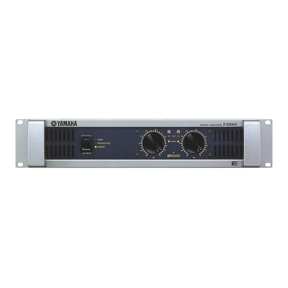
Page 6: Panel Layout
P5000S/P7000S ■ PANEL LAYOUT Front Panel q [POWER] switch and indicator q [POWER] w [TEMP] indicator w [TEMP] e [PROTECTION] indicator e [PROTECTION] r [CLIP] indicator r [CLIP] t [SIGNAL] indicator t [SIGNAL] y Volume control knobs ]indicator i Air intakes... - Page 7 P5000S/P7000S Rear Pane SPEAKERS LOW CUT WOOFER LOW CUT WOOFER STEREO BRIDGE PARALLEL FREQUENCY FREQUENCY INPUT BRIDGE q FILTER switch and[FREQUENCY] adjustment knob (One pair for each channel) ] ON/OFF switch e [INPUT] jacks (Channels A, B) r [STEREO/PARALLEL/BRIDGE] switch...
- Page 9 P5000S/P7000S Connector assembly is not a service parts. • Whole wiring drawing <Rev. 01> See page 10 See page 10 See page 10 This point has a wire harness tie. See page 9 See page 10 See page 11 See page 10...
- Page 10 P5000S/P7000S wert • Detail drawing * The following "wiring ass'y" are tied. (WD35970) (WD35970) (WD35950,WD35970) (WD35950,WD35960,WD35970) ATTENTION: Tie the wires (WD35970) at the side of switch. WD35970 Soldering (WD35980) ATTENTION: • Detail drawing (WD35960, WD35970) are through the CH00440. (TUBE L=180mm) WD35960,WD35970 (CH00440)<...
- Page 11 P5000S/P7000S • Detail drawing * The following "wiring ass'y" are tied. (WD36100,WD36110) J,H,B,CHN destination only. J,H,B,CHN • These wiring ass'y has to be tense condition from tie of No.9 to the tie of No.8. Need twist of three rotations. (WD36100,WD36110) !0 ! 3 ! 4 •...
- Page 12 P5000S/P7000S !1 ! 2 • Detail drawing The following "wiring ass'y" are tied. (WD35940,WD38950,WD36060x2 WD36070) • The wiring ass'y(WD35950) has to be tense condition from CN412 side to the tie of No.11. (WD36060x2,WD36070,FAN WIRING) • These wiring ass'y of fan has to be tense condition from fan side to the tie of No.12.
- Page 13 P5000S/P7000S • Connect of coils. * Regarding to connect the wire of coil. Please connect the Red wire to CN406. Please connect the Black wire to CN415.
-
Page 14: Disassembly Procedure
P5000S/P7000S ■ DISASSEMBLY PROCEDURE Rack Angle (Time required: about 1 min.) Remove the three (3) screws marked [430] for each side. The rack angle can then be removed. (Fig.1) Top Cover (Time required: about 2 min.) Remove the eleven (11) screws marked [480]. - Page 15 P5000S/P7000S PS Circuit Board (Time required: about 5 min.) Remove the rack angle. (See procedure 1.) Remove the top cover. (See procedure 2.) Remove the nine (9) screws marked [180]. The PS circuit board can then be removed. (Fig.3) [410] [180] [180]: Bind Head Tapping Screw-S 3.0X6 MFZN2BL (EP630210)
- Page 16 P5000S/P7000S [270] [280] [270] [280] [270]: Hex Spacer H=24.5 B=5.5 (WD490100) (Fig.5) [280]: Bind Head Tapping Screw-S 3.0X6 MFZN2BL (EP630210) + (Fig.4) OUT1 Circuit Board (Time required: about 4 min.) 6-1 Remove the rack angle. (See procedure 1.) 6-2 Remove the top cover. (See procedure 2.) 6-3 Remove the four (4) screws marked [320].
- Page 17 P5000S/P7000S Front Panel part (Time required: about 5 min.) Remove the rack angle. (See procedure 1.) Remove the top cover. (See procedure 2.) Cuts Cord Holder (5 Point) of the Connector assembly. (Fig.7) Remove the six (6) screws marked [410]. (Fig.2, Fig.3)
- Page 18 P5000S/P7000S Coil circuit board (Time required: about 7 min.) 10-1 Remove the front panel part. (See procedure 8.) 10-2 Remove the PS circuit board. (See procedure 4.) 10-3 Remove the four (4) screws marked [60]. The coil circuit board can then be removed.
- Page 19 P5000S/P7000S PSW Circuit Board (Time required: about 10 min.) 12-1 Remove the front panel part. (See procedure 8.) 12-2 Remove the power switch escutcheon marked [400]. (Fig.13) 12-3 It presses lightly from the panel back and remove the power switch knob marked [100].
- Page 20 P5000S/P7000S Disassemble of Front Panel 1 and Front Panel 2 (Time required: about 8 min.) 14-1 Remove the front panel part. (See procedure 8.) 14-2 Remove the handles. (See procedure 13.) 14-3 Remove the eight (8) hex socket tapping screws marked [360].
-
Page 21: Ic Block Diagram
P5000S/P7000S ■ IC BLOCK DIAGRAM • NJM2068MD-TE2 (X3505A00) Dual Operational Amplifier P5000S IN: IC301, IC302, IC303, IC304, IC305, IC306, IC307 PAH: IC201 P7000S IN: IC301, IC302, IC303, IC304, IC305, IC306, IC307 PAH: IC201 +DC Voltage Output A Supply Inverting Output B... -
Page 22: Circuit Boards
P5000S/P7000S ■ CIRCUIT BOARDS CONTENTS ● PAH Circuit Board (X3850B0) ..................23 ● PS Circuit Board (X5600A0) ..................25 ● IN Circuit Board (X3501C0) ..................29 ● LED Circuit Board (X3895C0) ..................30 ● OUT1 Circuit Board (X3895C0) ..................31 ●... - Page 23 P5000S/P7000S W403(Ach) ● PAH Circuit Board to PS- W408(Bch) W402(Ach) to PS- W407(Bch) W401(Ach) to PS- W406(Bch) CN412(Ach) to PS- W604(Ach) CN411(Bch) to OUT2- W606(Bch) to IN-CN301(Ach,Bch) A’ B’...
- Page 24 Q112 Q113 Q114 Q115 Q117N Q117P Q118N Q118P Q119N Q119P Q120N Q120P Q121N Component side A’ Q121P Q122N Q122P Q123N Q123P Q124N Q124P Q125N Q125P Q126N Q126P Q218 PR201 PR202 :Installed :not installed Pattern side B’ 2NAP-WD35140 (P5000S) 2NAP-WD35140 (P7000S)
- Page 25 P5000S/P7000S ● PS Circuit Board to PSW-W602(or W601) to LED-CN601 TEMP LED TEST POINT to FAN(Ach) to PAH-CN201(Ach) to PAH-CN201(Bch) to IN-CN301 to PAH-CN103(Bch) to PAH-CN105(Bch) to FAN(Bch) to PAH-CN105(Ach) to PAH-CN104(Bch) to PAH-CN104(Ach) FAN TEST POINT to PAH-CN103(Ach)
- Page 26 P5000S/P7000S to COIL-W701 to PSW-W603 to COIL-W702 to PSW-W601(or W602) to AC IN to AC IN Component Side...
- Page 27 P5000S/P7000S...
- Page 28 P5000S/P7000S Pattern Side PS: 2NAP-WD35180 1 (P5000S) PS: 2NAP-WD35180 1 (P7000S)
- Page 29 P5000S/P7000S ● IN Circuit Board to VR-CN602 PAH-CN202(Ach,Bch) PS-CN408 to OUT2-W301B Component Side Pattern Side 2NAP-WD35520...
- Page 30 P5000S/P7000S ● LED Circuit Board Pattern Side As for Ver B, some silk prints are different. Ver. B Component Side 2NAP-WD35390...
- Page 31 P5000S/P7000S ● OUT1 Circuit Board to OUT2-W607B Component Side Pattern Side As for Ver B, some silk prints are different. Ver. B 2NAP-WD35390...
- Page 32 P5000S/P7000S ● OUT2 Circuit Board to PAH-CN102(Ach) to IN-W301A to OUT1-W607A to PAH1-CN102(Bch) to PS-CN416 Component Side Pattern Side As for Ver B, some silk prints are different. Ver. B 2NAP-WD35390...
- Page 33 P5000S/P7000S ● PSW Circuit Board ● VR Circuit Board Power ON/OFF to IN-CN302 to PS-CN404 to PS-CN403 (or CN405) to PS-CN405 Component Side (or CN404) Component Side Pattern Side Pattern Side As for Ver B, some silk prints are different.
- Page 34 P5000S/P7000S ● COIL Circuit Board to PS-CN415 to PS-CN406 H destination Component side L701, L702 INSULOCK-TIE Put insulock-tie through the hols of PCB. Solder side Component Side Pattern Side 2NAP-WD35490...
- Page 35 P5000S/P7000S ■ INSPECTION Scope • This inspection specifications is applied to the powe r amplifier P5000S/P7000S. ∗ Refer to P42 “The switch and adjustment part” for details in the adjustment part. Preparation for STEREO/PARALLEL mode Attenuator : "0"(MAX) Input terminal...
- Page 36 P5000S/P7000S *SUB WOOFER position(OFF/SUB WOOFER/LOW CUT switch) <It sets [FREQUENCY] adjustment knob to 25Hz (Min.).> Input signal is 25Hz, -10dBu, and set FREQUENCY to 25Hz. The output voltage shall be -3.0 +/- 2.0dB compared to the 1kHz at the switch off.
- Page 37 P5000S/P7000S 3.10 Stability Input the rectangular waveform of 10kHz at -10dBu. Connect only capacitance of 0.01uF (Polyester film capacitance) to output terminal. Input signal is 10kHz, -10dBu sqare wave. The overshoot and the ringing should be as follows. Overshoot : Vp/Vo < 2.5 Ringing : Within 7 waves and no oscillation.
- Page 38 P5000S/P7000S Preparation For BRIDGE mode Attenuator :"0"(MAX) Effective only channel A. Input terminal : cannon connector 2PIN-HOT/3PIN-COLD/1PIN-GND MODE switch : BRIDGE SUBWOOFER/LOW CUT switch : OFF YS Processing switch : OFF Load resistor : 8+8 ohms +/- 1% Connection for measuring : Measure the output at the point as shown below.
- Page 39 P5000S/P7000S 5.4 Output Noise level Shunt the input terminal with 600 ohms (2pin-hot, 3pin-cold). The noise level of output terminal shall be less than -60 dBu. Next, set the input attenuator to MIN. The noise level shall be less than -65 dBu.
- Page 40 P5000S/P7000S 6.4 Repair concrete instance at the trouble part All secondary output isn't output. Check the following instruction. q Confirm the resistor value of R416, R451(6.8Ω 5 W). Exchange if open the resistor value. w Confirm the resistor value of Q406, Q407 Between C-E.
- Page 41 P5000S/P7000S ● Wurubg/Check Parts 10k 1/4W 10k 1/4W 22k 3W 22k 3W -15V +15V W407 W406 CN408 W408 R429 R430 IC403 W601 IC401 IC402 CN404 W603 VI(PK) SW601 R421 CN403 VI(PK) R451 Q407 R419 CN405 R420 R416 W602 Q406 PR401 CN406 ∗...
- Page 42 P5000S/P7000S The switch and adjustment part ● Rear side: MODE switch, YSProcessing switch SUBWOOFER/LOW CUT switch, FREQUENCY VR201(channel A) VR201(channel B) CN101(channel A) CN101(channel B) TM-C FAN-C Front side: TEMP TED, PROTECTION LED, POER LED, CLIP LED SIGNAL LED, YSProcessing LED, Attenuator...
- Page 43 P5000S/P7000S ■ 1) channel A 25Hz 2) channel A 150Hz 3) channel B 25Hz 4) channel B 150Hz...
- Page 44 P5000S/P7000S P5000S P7000S(J/U/V/A/T) P7000S(H/W/B/K/O) 500W+500W 700W+700W 650W+650W P5000S P7000S 250W 350W...
- Page 45 P5000S/P7000S P5000S P7000S 140 +/- 30W 140 +/- 30W P5000S P7000S 35 +/- 10W 35 +/- 10W P5000S P7000S 16 +/- 4V 18 +/- 4V...
- Page 46 P5000S/P7000S SPEAKERS MEASURING TERMINAL INSTRUMENT INPUT 8 ohms 8 ohms P5000S P7000S(J/U/V/A/T) P7000S(H/W/B/K/O) 63.25V 74.83V 72.11V...
- Page 47 P5000S/P7000S < 1-1> WD351800 PS70J AC100V/50Hz WD351900 PS70U AC120V/60Hz WD352000 PS70H AC230V/50Hz WD352100 PS70A AC240V/50Hz WD352200 PS70K AC230V/50Hz WD352300 PS50J AC100V/50Hz WD352400 PS50U AC120V/60Hz WD352500 PS50H AC230V/50Hz WD352600 PS50A AC240V/50Hz WD352700 PS50K AC230V/50Hz < 2-1> Model Load resistor P7000S W406RE-W407BL +150.8...
- Page 48 P5000S/P7000S...
- Page 49 P5000S/P7000S • 10k 1/4W 10k 1/4W 22k 3W 22k 3W -15V +15V W407 W406 CN408 W408 R429 R430 IC403 W601 IC401 IC402 CN404 W603 VI(PK) SW601 R421 CN403 VI(PK) R451 Q407 R419 CN405 R420 R416 W602 Q406 PR401 CN406 ∗...
- Page 50 P5000S/P7000S • Rear side: MODE switch, YSProcessing switch SUBWOOFER/LOW CUT switch, FREQUENCY VR201(channel A) VR201(channel B) CN101(channel A) CN101(channel B) TM-C FAN-C Front side: TEMP TED, PROTECTION LED, POER LED, CLIP LED SIGNAL LED, YSProcessing LED, Attenuator...
-
Page 51: Parts List
P5000S / P7000S POWER AMPLIFIER PARTS LIST CONTENTS OVERALL ASSEMBLY PAUNIT ELECTRICAL PARTS Note) DESTINATION ABBREVIATIONS Australian model Chinese model British model South-east Asia model Canadian model Taiwan model German model U.S.A. model European model General export model (110V) French model... - Page 52 P5000S / P7000S ■ OVERALL ASSEMBLY ∗ 80d and 80e are soldered with boad-in-connectors. 210 320 ∗ ∗ 30 5...
- Page 53 P5000S / P7000S PART NO. DESCRIPTION REMARKS REF NO. QTY RANK OVERALL ASSEMBLY P5000S_A/P7000S_A Overall Assembly P5000S_A J P5000S_A J (WD48630) Overall Assembly P5000S_A U P5000S_A U,V (WD48640) Overall Assembly P5000S_A H P5000S_A H,W (WD48650) Overall Assembly P5000S_A B P5000S_A B...
- Page 54 P5000S / P7000S DESCRIPTION REMARKS PART NO. QTY RANK REF NO. VQ049800 Bonding Tapping Screw-B 3.0X10 MFZN2BL EP600790 Flat Head Tapping Screw-B 3.0X8 MFZN2BL WD491100 ∗ Front Panel 1 P5000S_A PRINTED P5000S_A WD491000 ∗ Front Panel 1 P7000S_A PRINTED P7000S_A...
- Page 55 P5000S / P7000S ■ PA UNIT...
- Page 56 P5000S / P7000S DESCRIPTION REMARKS PART NO. QTY RANK REF NO. PA UNIT P5000S_A/P7000S_A WD490500 ∗ PA Unit P5000S_A J P5000S_A WD490400 ∗ PA Unit P7000S_A J P7000S_A Heat Sink P7000S_A (WD49030) WD490000 ∗ Spacer H=7.5 B=5.5 WD351600 ∗ Circuit Board...
- Page 57 P5000S / P7000S ■ ELECTRICAL PARTS DESCRIPTION REMARKS PART NO. QTY RANK REF NO. ELECTRICAL PARTS P5000S_A/P7000S_A WD354900 ∗ Circuit Board COIL P7000S_A J (X4945A0) WD355000 ∗ Circuit Board COIL P7000S_A H H,W,B,O (X4945A0) WD355200 Circuit Board IN P7000S_A (X3501C0) ∗...
- Page 58 P5000S / P7000S DESCRIPTION REMARKS PART NO. QTY RANK REF NO. RD356100 R317 Carbon Resistor (chip) 1.0K 63M J R318 RF356910 Carbon Resistor (chip) 9.1K D 1608 RD356100 R319 Carbon Resistor (chip) 1.0K 63M J RF356910 R320 Carbon Resistor (chip) 9.1K D 1608...
- Page 59 P5000S / P7000S DESCRIPTION REMARKS PART NO. QTY RANK REF NO. V8499100 C413 Electrolytic Cap. 2200 200V J,H,W,B,O,A,K C413 WB543200 Electrolytic Cap. 2800 200V U,V,T V8499100 C414 Electrolytic Cap. 2200 200V J,H,W,B,O,A,K WB543200 C414 Electrolytic Cap. 2800 200V U,V,T C415 FG644100 Electrolytic Cap.
- Page 60 P5000S / P7000S DESCRIPTION REMARKS PART NO. QTY RANK REF NO. V8629700 D406 Diode RL3ALF014-302 D407 V8629700 Diode RL3ALF014-302 WD543900 D408 Diode 1N4004 DO-41 WD543900 -411 Diode 1N4004 DO-41 D412 VN399500 Diode FMU-36S 20.0A 600V D413 V8498700 Diode FMU-36R 20.0A 600V...
- Page 61 P5000S / P7000S DESCRIPTION REMARKS PART NO. QTY RANK REF NO. VD678500 Q418 Digital Transistor DTA114ES Q419 V2797700 Transistor 2SC5395 E,F V2797600 Q420 Transistor 2SA1993 E,F V2797700 Q421 Transistor 2SC5395 E,F Q422 V2797600 Transistor 2SA1993 E,F Q423 VQ547200 Transistor 2SA1837 (HFE)
- Page 62 P5000S / P7000S DESCRIPTION REMARKS PART NO. QTY RANK REF NO. HF455330 R463 Carbon Resistor 330.0 1/4 J R464 HF456180 Carbon Resistor 1.8K 1/4 J HF456180 R465 Carbon Resistor 1.8K 1/4 J HF456820 R466 Carbon Resistor 8.2K 1/4 J R467...
- Page 63 P5000S / P7000S DESCRIPTION REMARKS PART NO. QTY RANK REF NO. V8499100 C417 Electrolytic Cap. 2200 200V U,V,T C417 WB543200 Electrolytic Cap. 2800 200V H,W,B,O,A,K WA862800 C418 Electrolytic Cap. 10.00 35.0V WB543800 C420 Polypropylene Capacitor 0.4700 400V J C420 WB544400 Polypropylene Capacitor 0.3900 400V J...
- Page 64 P5000S / P7000S DESCRIPTION REMARKS PART NO. QTY RANK REF NO. WA757600 -417 Diode AL01Z D418 WD543900 Diode 1N4004 DO-41 WA757600 D419 Diode AL01Z WA757600 D420 Diode AL01Z D421 VD631600 Diode 1SS133,176,HSS104 D422 VD631600 Diode 1SS133,176,HSS104 WD543900 D423 Diode 1N4004 DO-41...
- Page 65 P5000S / P7000S DESCRIPTION REMARKS PART NO. QTY RANK REF NO. V2797600 Q425 Transistor 2SA1993 E,F Q426 V2797700 Transistor 2SC5395 E,F V2797700 -429 Transistor 2SC5395 E,F HF457100 R401 Carbon Resistor 10.0K 1/4 J R402 HB027200 Metal Film Resistor 20.0K 1/4 F...
- Page 66 P5000S / P7000S DESCRIPTION REMARKS PART NO. QTY RANK REF NO. HF456180 R470 Carbon Resistor 1.8K 1/4 J R471 HF458120 Carbon Resistor 120.0K 1/4 J HF458120 R472 Carbon Resistor 120.0K 1/4 J HF458220 R473 Carbon Resistor 220.0K 1/4 J R474...
- Page 67 P5000S / P7000S DESCRIPTION REMARKS PART NO. QTY RANK REF NO. V2797700 Q605 Transistor 2SC5395 E,F Q606 VD678500 Digital Transistor DTA114ES VD678500 -609 Digital Transistor DTA114ES HF456510 R601 Carbon Resistor 5.1K 1/4 J R602 HF457150 Carbon Resistor 15.0K 1/4 J...
- Page 68 P5000S / P7000S DESCRIPTION REMARKS PART NO. QTY RANK REF NO. V9726300 C127 Electrolytic Cap. 470.00 10.0V C128 V9727800 Electrolytic Cap. 22.00 50.0V US062470 C129 Ceramic Capacitor-SL(chip) 470P 50V J US064100 C201 Ceramic Capacitor-B (chip) 0.0100 50V K C202 US062100...
- Page 69 P5000S / P7000S DESCRIPTION REMARKS PART NO. QTY RANK REF NO. WD408800 L105 Coil 1.7U ∗ Q101 VR152800 Transistor 2SA1480 E,F VR152900 Q102 Transistor 2SC3790 E,F V8093400 Q103 Transistor 2SC3425 Q104 V8093300 Transistor 2SA1924 Q105 VU418600 Transistor 2SC3468 D,E VU418400...
- Page 70 P5000S / P7000S DESCRIPTION REMARKS PART NO. QTY RANK REF NO. HV754220 R128 Flame Proof C. Resistor 22.0 1/4 J R129 V4833200 Wire Wound Resistor 0.22 5W K V4833200 R130 Wire Wound Resistor 0.22 5W K HV753470 R131 Flame Proof C. Resistor 4.7 1/4 J...
- Page 71 P5000S / P7000S DESCRIPTION REMARKS PART NO. QTY RANK REF NO. RD354750 R209 Carbon Resistor (chip) 75.0 63M J R210 RD356820 Carbon Resistor (chip) 8.2K 63M J RD355100 R211 Carbon Resistor (chip) 100.0 63M J RD356820 R212 Carbon Resistor (chip) 8.2K 63M J...
- Page 72 P5000S / P7000S DESCRIPTION REMARKS PART NO. QTY RANK REF NO. UA653220 C106 Mylar Capacitor 2200P 50V J C107 WD706100 ∗ Ceramic Capacitor-SL 33P 1KV J WD705700 C108 ∗ Ceramic Capacitor-SL 10P 1KV J VV082300 C109 Mylar Capacitor 0.1000 250V M...
- Page 73 P5000S / P7000S DESCRIPTION REMARKS PART NO. QTY RANK REF NO. VJ657300 D122 Diode AK03 V0 D123 VJ657300 Diode AK03 V0 VQ469600 D128 Diode HSS82 VQ469600 D129 Diode HSS82 D201 VT332900 Diode 1SS355 TE-17 D202 VT332900 Diode 1SS355 TE-17 VD631600...
- Page 74 P5000S / P7000S DESCRIPTION REMARKS PART NO. QTY RANK REF NO. HV753470 R107 Flame Proof C. Resistor 4.7 1/4 J R108 HV753470 Flame Proof C. Resistor 4.7 1/4 J HF457560 R109 Carbon Resistor 56.0K 1/4 J HF457560 R110 Carbon Resistor 56.0K 1/4 J...
- Page 75 P5000S / P7000S DESCRIPTION REMARKS PART NO. QTY RANK REF NO. HV754100 R177 Flame Proof C. Resistor 10.0 1/4 J R178 HV754100 Flame Proof C. Resistor 10.0 1/4 J HV755330 R179 Flame Proof C. Resistor 330.0 1/4 J VC762900 R180 Metal Oxide Film Resistor 3.9K 2W J...
- Page 76 P5000S / P7000S DESCRIPTION REMARKS PART NO. QTY RANK REF NO. RF357200 R280 Carbon Resistor (chip) 20.0K D 1608 R281 RD357100 Carbon Resistor (chip) 10.0K 63M J RF357620 R282 ∗ Carbon Resistor (chip) 62.0K D 1608 HB028270 R283 Metal Film Resistor 270.0K 1/4 F...
- Page 77 P5000S / P7000S POWER AMPLIFIER ■ CONTENTS IC & DIODE OUTSIDE FIGURE BLOCK DIAGRAM WIRING DIAGRAM OVERALL CIRCUIT DIAGRAM IN ...................... C3 PAH 1/2 ..................... C4 PAH 2/2 ..................... C5 PS ..................... C6 LED, OUT1, OUT2, COIL, VR, PSW ..........C7 ■...
- Page 78 P5000S / P7000S IC & DIODE OUTSIDE FIGURE • NJM7815FA (XD853A00) • NJM7915FA (XD854A00) • FMU-36S (VN399500) • FMU-36R (V8498700) REGULATOR +15V REGULATOR -15V DIODE STACK 20.0A 600V DIODE STACK 20.0A 600V PS: IC405 PS: D412 PS: IC403, IC404 PS: D413...
- Page 79 <C.1> P5000S/P7000S P5000S / P7000S BLOCK DIAGRAM from PS from W401 from W402 from W403 CN103 CN105 W301B W301A STATE VARIABLE ACTIVE FILTER CN104 CHANNEL A B(RE) -B(WH) OUT 2 (BL) GND(BL) (BL) CN301-8P SW303-1/2 IC304-1/2 IC304-2/2 IC305-1/2 IC305-2/2 CN202-3P...
- Page 80 <C.2> P5000S/P7000S P5000S / P7000S WIRING COIL J/H distination only PA H H B ch A ch (PK) J/H distination only OUT2 OUT1 28C99-8833621 ∗ Connector assembly is not a service parts. P5000S/P7000S P5000S/P7000S <C.2>...
- Page 81 <C.3> P5000S/P7000S P5000S / P7000S OVERALL CIRCUIT DIAGRAM 1/5 (IN) FREQUENCY Ach ∗ SW301 STEREO STEREO BRIDGE BRIDGE INPUT PARALELL PARALELL OP AMP OP AMP OP AMP OP AMP OP AMP INPUT 3.9K OP AMP OP AMP 3.9K to VR-CN602...
- Page 82 <C.4> P5000S/P7000S P5000S / P7000S OVERALL CIRCUIT DIAGRAM 2/5 (PAH 1/2) to C5-L1 to C5-L3 to C5-L3 to IN-CN301 1P(Ach) to IN-CN301 3P(Bch) to IN-CN301 2P(Ach) to IN-CN301 4P(Bch) OP AMP to C5-L5 to PS-CN411(Bch) to PS-CN412(Ach) to C5-L6 OP AMP...
- Page 83 <C.5> P5000S/P7000S P5000S / P7000S OVERALL CIRCUIT DIAGRAM 3/5 (PAH 2/2) from C4-A1 from C4-A1 from C4-A2 not connected to PS-W401 (Ach) to PS-W406 (Bch) from C4-A5 to PS-W402 (Ach) to PS-W407 (Bch) to PS-W403 (Ach) to PS-W408 (Bch) from C4-A4...
- Page 84 <C.6> P5000S/P7000S P5000S / P7000S OVERALL CIRCUIT DIAGRAM 4/5 (PS) to PSW-W603 to AC (PK) to PSW-W601(or W602) to PSW-W602(or W601) to OUT2-W605 to PAH-CN103(Ach) to PAH-CN104(Ach) REGULATOR +15V to PAH-CN105(Ach) to PAH-CN103(Bch) to PAH-CN104(Bch) to PAH-CN105(Bch) REGULATOR +15V to IN-CN301...
- Page 85 <C.7> P5000S/P7000S P5000S / P7000S OVERALL CIRCUIT DIAGRAM 5/5 (LED, OUT1, OUT2, COIL, VR, PSW) OUT2 OUT1 WD36080 to PAH-CN102(A) to PS-CN410 to PS-CN416 SPEAKERS WD36010 CHANNEL A CHANNEL B to PAH-CN102(B) WD36090 28CC1-8833618 28CC1-8833618 to IN-W301A COIL to PS-CN406...
Need help?
Do you have a question about the P5000S and is the answer not in the manual?
Questions and answers