Philips HTS5540 Service Manual
Dvd home theater system
Hide thumbs
Also See for HTS5540:
- Service manual (47 pages) ,
- Quick start manual (8 pages) ,
- User manual (23 pages)
Advertisement
Table of Contents
- 1 Specifications
- 2 Block Diagram
- 3 Wiring Diagram
- 4 FTD Display Pin Assignment
- 5 Circuit Diagram
- 6 Main Board
- 7 CIRCUIT DIAGRAM - Part One
- 8 CIRCUIT DIAGRAM - Part Two
- 9 Pcb Layout - Top View
- 10 Pcb Layout - Bottom View
- 11 Power Board
- 12 Amp Board
- 13 VOL+USB+MP3 Board
- 14 Touch Board
- 15 Jack Board
- Download this manual
See also:
User Manual
DVD Home Theater System
Service
Service
Service
Service Manual
©
Copyright 2010 Philips Consumer Electronics B.V. Eindhoven, The Netherlands
All rights reserved. No part of this publication may be reproduced, stored in a retrieval system or
transmitted, in any form or by any means, electronic, mechanical, photocopying, or otherwise
without the prior permission of Philips.
Published by
RY1010
Service Audio Printed in The Netherlands Subject to modification
Version 1.0
TABLE OF CONTENTS
Location of PCB Boards ............................................ 1-2
Versions Variation ...................................................... 1-2
Specifications ............................................................ 1-3
Measurement Setup .................................................. 1-4
Service Aids .............................................................. 1-5
ESD & Safety Instruction .......................................... 1-6
Lead-free soldering Information ................................ 1-7
Setting procedure & Repair Instructions........................ 2
Disassembly Instructions & Service positions .............. 3
Block & Wiring Diagram ................................................ 4
VFD Board .................................................................... 5
Main Board .................................................................... 6
Power Board .................................................................. 7
AMP Board .................................................................... 8
VOL+USB+MP3 Board .................................................. 9
Touch Board ................................................................ 10
Jack Board .................................................................. 11
Mechanical Exploded view .......................................... 12
Revision List ................................................................ 13
1 - 1
Chapter
HTS5540
/93/94/51
HTS5550
/93/94/51
3139 785 35260
GB
Advertisement
Table of Contents

Related Manuals for Philips HTS5540


Summary of Contents for Philips HTS5540
- Page 1 Revision List ..............13 © Copyright 2010 Philips Consumer Electronics B.V. Eindhoven, The Netherlands All rights reserved. No part of this publication may be reproduced, stored in a retrieval system or transmitted, in any form or by any means, electronic, mechanical, photocopying, or otherwise without the prior permission of Philips.
-
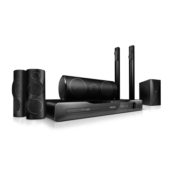
Page 2: Specifications
1 - 3 SPECIFICATIONS Playback media Dimensions (WxHxD): Center ............280 x 95 x 92 (mm) DVD-Video, DVD+R/+RW, DVD-R/-RW, DVD+RDL, CD-R/CD- Speaker ..........100 x 280 x 115 (mm) RW, Audio CD, Video CD/SVCD,Picture CD, MP3-CD, WMA- Tall speaker .......... 260 x 1101 x 260 (mm) CD, DivX-CD, USB storage device Weight: Center ................ - Page 3 2 - 1 2 - 1 Software upgrade & Procedure to restore product setting 1)Restore factory setting 8) How to replace the defective DVD loader module a) Press <SETUP> button on R/C a) Copy the latest upgrading software onto a CD-R or USB storage a) Remove the defective DVD loader module.
- Page 4 2 - 2 2 - 2 REPAIR INSTRUCTIONS (One)
- Page 5 2 - 3 2 - 3 REPAIR INSTRUCTIONS (Two)
- Page 6 2 - 4 2 - 4 REPAIR INSTRUCTIONS (Three)
-
Page 7: Block Diagram
4 - 1 4 - 1 BLOCK DIAGRAM... -
Page 8: Wiring Diagram
4 - 2 4 - 2 WIRING DIAGRAM JACK PCB AMP PCB MAIN PCB POWER PCB VFD PCB TOUCH PCB... -
Page 9: Ftd Display Pin Assignment
5 - 1 5 - 1 FTD DISPLAY PIN ASSIGNMENT VFD BOARD TABLE OF CONTENTS FTD Display Pin Assignment ............. 5-1 Circuit Diagram ................. 5-2 PCB Layout Top & Bottom View ............5-3 PIN CONNECTION... -
Page 10: Circuit Diagram
5 - 2 5 - 2 CIRCUIT DIAGRAM C392 ZD312 A1 C391 DP351 A3 C381 C385 Q352 R3052 B1 R3055 B1 R3058 B1 RB357 B1 C389 R3060 B2 R3061 A1 C387 R3067 A2 R3068 A3 C382 C386 Q352 R3053 B1 R3056 B1 R3059 B1 SN351 B1... -
Page 11: Main Board
6 - 1 6 - 1 INTERNAL IC DIAGRAM - MT1389FEX/SN DVB-T HDMI1.2Tx RGB video Module CVBS MT1389S MAIN BOARD FLASH 8ch Audio SPDIF Front-panel USB2.0/3 in 1 card DRAM Remote reader TABLE OF CONTENTS Internal IC Diagram ................6-1 Circuit Diagram(part one) .............. -
Page 12: Circuit Diagram - Part One
6 - 2 6 - 2 CIRCUIT DIAGRAM - part one C801 R813 C242 FB226 A2 R834 C719 L702 R706 Q703 C1206 B1 FB212 B1 R804 C830 R839 C205 R225 C1210 C1 CE802 C1 R1210 C1 R601 R213 R285 R298 IC206 C4 C803 R816... -
Page 13: Circuit Diagram - Part Two
6 - 3 6 - 3 CIRCUIT DIAGRAM - part two C1213 A1 R1223 A1 R348 IC305 C1200 A3 R335 R505 R523 C901 R352 C931 C936 C510 FB304 B4 R3030 B4 C930 CE313 C1 CE330 C1 R911 R3007 C2 IC303 R555 R367 C1214 A1... -
Page 14: Pcb Layout - Top View
6 - 4 6 - 4 PCB LAYOUT - TOP VIEW C1203 A1 Q701 A1 R714 A1 FB225 A2 R731 A2 JK302A A3 R368 A3 R3027 A4 C940 B1 R250 B1 R209 B2 C340 B3 IC303 B3 ZD302 B3 C929 B4 R332 B4 R549 B4 C819 C1... -
Page 15: Pcb Layout - Bottom View
6 - 5 6 - 5 PCB LAYOUT - BOTTOM VIEW C1200 A1 C0222 A2 FE306 A2 C1217 A3 R1229 A3 R548 CE327 B1 C0209 B2 C0221 B2 C0248 B2 C826 FB707 B2 C309 R3019 B3 CE319 B4 R547 CE206 C2 CE805 C2 C250 CE212 C3... -
Page 16: Power Board
7 - 1 7 - 1 INTERNAL IC DIAGRAM - AZ431 CATHODE POWER BOARD ANODE TABLE OF CONTENTS Internal IC Diagram ................7-1 Circuit Diagram .................. 7-2 PCB Layout Top View ............... 7-3 PCB Layout Bottom View ..............7-4 INTERNAL IC DIAGRAM - AZ7500BP OUTPUT CTRL Oscillator Pulse-Steering... - Page 17 7 - 2 7 - 2 CIRCUIT DIAGRAM BD901 A1 TVR903 A1 R949 C970 L908 R976 R953 C918 R906 D903 R943 C930 D923 R922 R995 Q922 C903 J906 IC904 R986 R936 C904 C910 R950 C971 R908 ZD908 A3 R954 C919 R910 D905 R990...
-
Page 18: Amp Board
8 - 1 8 - 1 INTERNAL IC DIAGRAM - TA5508APAG AMP BOARD TABLE OF CONTENTS Internal IC Diagram ................8-1 INTERNAL IC DIAGRAM - TAS5352 2ADDV Circuit Diagram .................. 8-2 PCB Layout Top & Bottom View ............8-3 System Microcontroller BST_A Bootstrap... - Page 19 8 - 2 8 - 2 CIRCUIT DIAGRAM C5001 L5015 JK5001 A2 C5121 C5214 R5175 C5196 R5194 C5090 R5093 C5077 R5103 C5102 R5106 IC5004 B4 C5133 FB5004 C1 R5165 C5158 R5117 Q5005 C3 R5153 R5043 C5002 L5015 L5009 C5122 L5012 R5176 C5197 C5014...
- Page 20 8 - 3 8 - 3 PCB LAYOUT - TOP VIEW C5068 R5123 C5052 C5108 C5073 C5173 R5128 C5055 C5109 C5077 C5177 R5129 C5056 C5112 C5094 D5005 R5130 C5057 C5113 C5095 IC5007 A1 R5131 C5062 C5128 C5098 IC5007 A1 R5135 C5064 C5129 C5099...
- Page 21 8 - 4 8 - 4 PCB LAYOUT - BOTTOM VIEW FB5001 A1 R5083 R5220 R5084 R5221 R5133 C5166 R5160 C5185 R5187 C5186 R5195 C5187 ZD5001 C1 C5190 ZD5002 C1 C5191 C5105 D5007 R5009 R5146 C5001 R5147 C5005 R5149 C5006 R5151 C5008 R5175...
-
Page 22: Vol+Usb+Mp3 Board
9 - 1 9 - 1 VOL+USB+MP3 BOARD TABLE OF CONTENTS Circuit Diagram .................. 9-2 PCB Layout Top View ............... 9-3 PCB Layout Bottom View ..............9-4... - Page 23 9 - 2 9 - 2 CIRCUIT DIAGRAM FB11 FB16 JK11 RB17 VR11 FB12 FB17 JK12 RB15 USB11 A3...
-
Page 24: Touch Board
10 - 1 10 - 1 TOUCH BOARD TABLE OF CONTENTS Circuit Diagram .................. 10-2 PCB Layout Top View & Bottom View ..........10-3... - Page 25 10 - 2 10 - 2 CIRCUIT DIAGRAM...
-
Page 26: Jack Board
11 - 1 11 - 1 JACK BOARD TABLE OF CONTENTS Circuit Diagram .................. 11-2 PCB Layout Top View & Bottom View ..........11-3... - Page 27 11 - 2 11 - 2 CIRCUIT DIAGRAM CN103 A1 JK102 Q104 Q105 Q106 Q107 Q108...