Table of Contents
Advertisement
Quick Links
CONTENTS
To Service Personnel ..................................... 1~2
GX-500 PANELS ....................................................... 3~4
Gx-500Vcd Panels ................................................... 5
Specifications ......................................................... 6
Internal View .......................................................... 7
Disassembly Procedures ............................ 8~12
Volume Range ....................................................... 13
System Control Check ..................................... 13
Test Mode ................................................................ 14
System Test Mode ................................................ 14
Receiver Test Mode ...................................... 15~16
Tape Test Mode ..................................................... 16
Cd Test Mode ......................................................... 17
All Function Test Mode .................................... 18
1 0 0 6 7 2
MINI COMPONENT SYSTEM
GX-500VCD
GX-500VCD is composed of GX-500VCD and NX-GX500.
This manual has been provided for the use of authorized YAMAHA Retailers and their service personnel.
It has been assumed that basic service procedures inherent to the industry, and more specifically YAMAHA Products, are
already known and understood by the users, and have therefore not been restated.
WARNING:
Failure to follow appropriate service and safety procedures when servicing this product may result in
personal injury, destruction of expensive components, and failure of the product to perform as specified.
For these reasons, we advise all YAMAHA product owners that any service required should be performed
by an authorized YAMAHA Retailer or the appointed service representative.
IMPORTANT:
The presentation or sale of this manual to any individual or firm does not constitute authorization, certifica-
tion or recognition of any applicable technical capabilities, or establish a principle-agent relationship
of any form.
The data provided is believed to be accurate and applicable to the unit(s) indicated on the cover. The research, engineering, and
service departments of YAMAHA are continually striving to improve YAMAHA products. Modifications are, therefore,
inevitable and specifications are subject to change without notice or obligation to retrofit. Should any discrepancy appear to
exist, please contact the distributor's Service Division.
WARNING:
Static discharges can destroy expensive components. Discharge any static electricity your body may have
accumulated by grounding yourself to the ground buss in the unit (heavy gauge black wires connect to this
buss).
IMPORTANT:
Turn the unit OFF during disassembly and part replacement. Recheck all work before you apply power to the
unit.
GX-500
SERVICE MANUAL
GX-500 is composed of GX-500 and NX-GX500.
IMPORTANT NOTICE
Cd Error Messages ............................................ 18
Cd Standard Operation Chart ................ 19~22
Adjustments .................................................... 23~25
Ic Data ................................................................ 26~32
Display Data .................................................... 33~34
Block Diagram ................................................ 35~39
Printed Circuit Board ................................. 40~62
Pin Connection Diagram ................................... 63
SCHEMATIC DIAGRAM ....................................... 64~71
Parts List ........................................................ 72~103
Grease Application Diagram ................ 104~105
GX-500 REMOTE CONTROL TRANSMITTER ........ 106
Gx-500Vcd Remote Control Transmitter .... 107
NX-GX500 .................................................................. 108
GX-500/GX-500VCD
Advertisement
Table of Contents

Related Manuals for Yamaha GX-500


Summary of Contents for Yamaha GX-500
-
Page 1: Mini Component System
This manual has been provided for the use of authorized YAMAHA Retailers and their service personnel. It has been assumed that basic service procedures inherent to the industry, and more specifically YAMAHA Products, are already known and understood by the users, and have therefore not been restated. - Page 2 GX-500/GX-500VCD TO SERVICE PERSONNEL 1. Critical Components Information. AC LEAKAGE Components having special characteristics are marked and EQUIPMENT WALL TESTER OR must be replaced with parts having specifications equal to OUTLET UNDER TEST EQUIVALENT those originally installed. 2. Leakage Current Measurement (For 120V Models Only).
- Page 3 GX-500/GX-500VCD B, G, R, L, T models B, G, R, L, T models English THIS PRINTING (SEE POSITION SHOWN IN THE ILLUSTRATION) INFORMS THE USER THAT THE APPARATUS CONTAINS A LASER COMPONENT. THIS LABEL (SEE POSITION SHOWN IN THE ILLUSTRATION) WARNS THAT ANY FURTHER PROCEDURE WILL BRING THE USER INTO EXPOSURE WITH THE LASER BEAM.
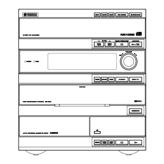
- Page 4 GX-500/GX-500VCD GX-500 PANELS B, G models U, C, R, A models NX-GX500 200(7-7/8")
- Page 5 GX-500/GX-500VCD R model U, C models A model B, G models...
- Page 6 GX-500/GX-500VCD GX-500VCD PANELS NX-GX500 200(7-7/8") L model R, T models...
-
Page 7: Specifications
(approx. 1W when set to the standby mode) 1kHz, 0.9% THD, 6Ω ........80W + 80W Dimensions (W X H X D) 1kHz, 10% THD, 6Ω ........100W + 100W GX-500 ..........280 X 320 X 364mm Input Sensitivity/Impedance (11” X 12-5/8” X 14-5/16”) AUX/MD ............200mV/47kΩ... - Page 8 P.C.B. MAIN (2) y P.C.B. MAIN (3) u P.C.B. MAIN (6) i DECK MECHANICAL UNIT Left side o GX-500 P.C.B. INPUT (3) GX-500VCD P.C.B. INPUT (2) !0 GX-500 CD MECHANICAL UNIT GX-500VCD VCD MECHANICAL UNIT !1 GX-500 P.C.B. CD GX-500VCD P.C.B.
- Page 9 GX-500/GX-500VCD DISASSEMBLY PROCEDURES (Remove parts in the order as numbered.) 1. Removal of Top Cover Top Cover Remove 11 screws ( q ) in Fig. 1. 2. Removal of CD/VCD Mechanical Unit a. Disconnect the power cord from the AC outlet.
- Page 10 GX-500/GX-500VCD 5. Operation Check of P.C.B. CD/VCD a. Remove the CD Mechanical Unit. b. Remove 4 screws ( y ) and then remove the P.C.B. CD/VCD in Fig. 4. c. Place blocks (at 3 locations) to hold the CD Mechanical Unit horizontally as shown in the Fig.
- Page 11 GX-500/GX-500VCD 6. Operation Check of P.C.B. Main (1) a. Remove the CD Mechanical Unit. b. Remove the Panel Unit. c. Remove the Deck Mechanical Unit. d. Remove 5 screws ( u ) in Fig. 6. e. Remove 1 screw ( i ) and then remove the P.C.B. Main (2) in Fig. 7.
- Page 12 GX-500/GX-500VCD 7. Removal of Tray & Traverse Unit a. Remove 4 screws ( ! 1 ) and then remove the Clamp Bracket in Fig. 10. b. Remove 2 screws ( !2 ) and then remove the Tray Brackets in Fig. 10.
- Page 13 GX-500/GX-500VCD 8. Removal of Pick-up Head 9. Removal of Cassette Mechanism a. Remove the Gear A in Fig. 12. Remove 4 screws ( !4 ) and then pull out the Cassette b. Pull out the Sled Shaft and remove the Pick-up Head Mechanism in Fig.
- Page 14 GX-500/GX-500VCD VOLUME RANGE DISPLAY DISPLAY DISPLAY – ∞ VOL MIN VOL 10 –55 VOL 56 –9 VOL 01 –79 VOL 57 –8 VOL 11 –54 VOL 02 –73 VOL 58 –7 VOL 03 –68 VOL 59 –6 VOL 04 –64 VOL 60 –5...
- Page 15 GX-500/GX-500VCD TEST MODE To facilitate inspection, measurement and location of any faulty point, 6 types of built-in Test Mode are provided, one for each section. • System Test Mode : Test mode for the system section. It is also used when entering the test mode for each section.
- Page 16 GX-500/GX-500VCD RECEIVER TEST MODE When RECEIVER TEST MODE is set through SYSTEM TEST MODE, “01 G.E.TEST” appears on the FL display. (01 is the test program No.) Test programs from 01 to 25 are incorporated in RECEIVER TEST MODE. Operation Procedure (Selection/execution of Test Program) 1) Select the test program by pressing the rTAPE (up) or eTAPE (down) button.
- Page 17 GX-500/GX-500VCD Equalizer test mode (Test program No. 01) When the equalizer test mode is set, “GEQ - xxx” is displayed. “xxx” represents the 3 band value of GEQ. It is possible to set the GEQ value directly, using the buttons on the remote control unit.
- Page 18 GX-500/GX-500VCD CD TEST MODE When CD TEST MODE is set through SYSTEM TEST MODE, “00STM100: 00” appears on the FL display. The CD TEST MODE is enabled. Each button operates as follows for each mode. The MODE No. is increased by pushing button.
- Page 19 GX-500/GX-500VCD ALL FUNCTION TEST MODE When ALL FUNCTION TEST MODE is set through SYSTEM TEST MODE, “AUX Digital” appears on the FL display. The operation condition in this mode will be as follows. • AUX/MD is used as the input source of the receiver section, which is then set to the Dolby Pro Logic mode (GX- 500VCD only).
- Page 20 GX-500/GX-500VCD CD STANDARD OPERATION CHART Press OPEN/CLOSE key. “OPEN” appears in the TIME indicator. Forced feed return operation. “TRV” signal is output until detection of LIMIT switch. Clamp down operation. Disc table reset. Tray open. Tracking Offset auto ADJ. (only POWER ON) Focus Offset auto ADJ.
- Page 21 GX-500/GX-500VCD * TOC READ * ~ Data fetch cycle ~ TRACK No. “1” is searched. : MUTE = “L” → “H”, After searching the beginning, MUTE is cancelled. “0:00” appears in the time indicator (IC11, 64 pin) ~ PLAY ~ Set to SEARCH by means of Y, T key.
- Page 22 GX-500/GX-500VCD HOME operation CLOSE operation Start Start LOAD MOTOR reverse rotate 10sec timer start LOAD SW LOAD MOTOR forward rotate OFF ? LOAD SW TIMER 10ms ON ? LOAD SW 10sec timer TIMER 10ms OFF ? time up ? LOAD MOTOR STOP...
- Page 23 GX-500/GX-500VCD ROTARY TRAY initialization operation Start 10sec timer start ROTARY MOTOR forward rotate 10sec timer time up ? POSITION SW OFF ? ROTARY MOTOR STOP Timer 20ms ERROR POSITION SW OFF ? 10sec timer time up ? POSITION SW ON ?
- Page 24 GX-500/GX-500VCD ADJUSTMENTS (DECK SECTION ONLY) 1. Before adjustment CT-160L (TX911120) ........FF/REW Since head magnetization, dust accumulations, etc. 3. Test tape required are likely to introduce error in the various character- istics, it is very important that the heads are properly MTT-111N (TX911650) ......
- Page 25 GX-500/GX-500VCD “MECHANICAL ADJUSTMENT” Item to be Instrument Adjustment Step Tape Mode Rating Remarks Adjusted required part Check each CT-160L (FF, REW) Torque FF REW FF, REW torque : within 70 ~ 160g/cm. torque meter TW-2111A (FWD) PLAY Take up torque : 30 ~ 70g/cm.
- Page 26 GX-500/GX-500VCD < Recording section > Item to be Instrument Measurement Points of Adjustment Step Tape Mode Rating Adjusted required conditions measurement parts Recording AC-514 VR6 (L ch) ACVM Input 1 kHz Signal to REC OUT Adjust for equal record and...
- Page 27 GX-500/GX-500VCD IC DATA IC5 : MN662741RPB1 [P.C.B. CD/VCD] Signal Processor & Controller 58 59 79 77 20 63 19 61 49 52 8 7 9 78 76 44 46 45 47 48 52 53 50 51 15 14 80 69 68...
- Page 28 GX-500/GX-500VCD IC5 : MN662741RPB1 [P.C.B. CD/VCD] Signal Processor & Controller Pin No. Name Function Reference voltage for D/A output section (TVD, ECS, TRD, FOD, FBAL, TBAL, TOFS) VREF FBAL Focus balance adjustment output TBAL Tracking balance adjustment output Focus error signal input...
- Page 29 GX-500/GX-500VCD IC11 : M38199EF [P.C.B. CD/VCD] µ 8 bit -COM (CD CPU) P87/SEG15 P16/DIG14 P86/SEG14 P17/DIG15 P85/SEG13 P20/DIG16 P84/SEG12 P21/DIG17 P83/SEG11 P22/DIG18 P82/SEG10 P23/DIG19 P81/SEG9 P80/SEG8 PA7/SEG7 PA6/SEG6 PA5/SEG5 X OUT PA4/SEG4 X IN PA3/SEG3 PB0/XC OUT PA2/SEG2 PB1/XC IN...
- Page 30 GX-500/GX-500VCD IC11 : M38199EF [P.C.B. CD/VCD] µ 8 bit -COM (CD CPU) Pin No. Port Name Function Open INT1 BLKCK Q-code read OK signal INT4 Open INT3 Open Decoder interrupt signal (GX-500VCD only) INT2 /HINT DEPH De-emphasis control (GX-500VCD only) System µ-COM data automatic transfer initialize, start signal...
- Page 31 GX-500/GX-500VCD IC11 : M38199EF [P.C.B. CD/VCD] µ 8 bit -COM (CD CPU) Pin No. Port Name Function Not used Not used Not used Not used Not used Not used Not used Not used Not used Not used Not used Not used...
- Page 32 GX-500/GX-500VCD IC8 : M38199EF [P.C.B. INPUT] µ 8 bit -COM (SYSTEM CPU) Port Name Function MDRES MD RESET INT1 ACIN POWER DOWN AC PULSE IN INT4 MD POWER DOWN INT3 OPEN INT2 REMO REMOTE CONTROL SIGNAL IN STEIN TUNER STEREO/MONO DETECT...
- Page 33 GX-500/GX-500VCD IC8 : M38199EF [P.C.B. INPUT] µ 8 bit -COM (SYSTEM CPU) Port Name Function HEAD PHONE DETECT [L : HP DETECT] MIC DETECT CASS CASSETTE IN DETECT PLSW DECK MECHA PLAY POSITION DETECT CrO2 (70 µs) POSITION DETECT CRO2...
- Page 34 GX-500/GX-500VCD DISPLAY DATA V801 : 16-BT-63GK (V2959000) PATTERN AREA PIN CONNECTION Pin No. Connection F1 NP NP P35 P34 P33 P32 P31 P30 P29 P28 P27 P26 P25 P24 P23 P22 P21 P20 P19 P18 P17 P16 P15 P14 P13 P12 P11 P10 Pin No.
- Page 35 GX-500/GX-500VCD ANODE CONNECTION...
- Page 36 GX-500/GX-500VCD BLOCK DIAGRAM...
- Page 37 GX-500/GX-500VCD BLOCK DIAGRAM DECK D.OUT CB402 TRAVERSE UNIT CASSETTE MECHA IC10 MUTE TAPE REC Q9,10 R/P HEAD REC LEVEL HEAD Q35,36 VIDEO IC8 76 TPEQ VR5,6 SERVO SIGNAL Q403,404 DOLBY PROCESSOR R/P AMP AN8806SB MUTE DF.DAC PB LEVEL VR1,4 TAPE PB...
- Page 38 GX-500/GX-500VCD BLOCK DIAGRAM IC11 MUTE SMUTE IC8 59 5.0V HP,IC8 85 MUTE HP JACK TUNER Q801 JK803 INPUT Q802 SWITCH TAPE POWER AMP IC201 HP AMP TE201 IC10 RY201 MUTE MUTE Q201 9,10 Q29,30 Q23.24 Q202 VOLUME LEVEL CONTROL SPEAKER ±HB...
- Page 39 GX-500/GX-500VCD PRINTED CIRCUIT BOARD (Foil side) CIRCUIT CHANGES BY MARKET. U, C, R, T, L, A B, G P.C.B. TUNER P.C.B. TUNER (Lead Type Device) (Surface Mount Device) D6 ~ 8, 10 L7 ~ 9 C68, 71 ~ 74 C46, 52 ~ 54...
- Page 40 GX-500/GX-500VCD PRINTED CIRCUIT BOARD (Foil side) GX-500 P.C.B. CD (Lead Type Device) GX-500 P.C.B. CD (Surface Mount Device) FROM: MOTOR UNIT FROM: PICK UP HEAD (LOADING) LIMITSW LIMITSW FEED- FEED+ SPD- SPD+ ROTARY+ ROTARY- ADRESS SW ADRESS SW STOP SW...
- Page 41 GX-500/GX-500VCD PRINTED CIRCUIT BOARD (Foil side) GX-500VCD P.C.B. VCD(1) (Surface Mount Device) GX-500VCD P.C.B. VCD(1) (Lead Type Device) FROM: MOTOR UNIT FROM: PICK UP HEAD (LOADING) LIMITSW LIMITSW FEED- FEED+ SPD- SPD+ ROTARY+ ROTARY- ADRESS SW ADRESS SW STOP SW...
- Page 42 GX-500/GX-500VCD PRINTED CIRCUIT BOARD (Foil side) GX-500 P.C.B. INPUT(3) GX-500 P.C.B. INPUT(1) (Lead Type Device) (Lead Type Device) HP.GND FROM : OPERATION(3) HP.R HPIN HP.L HP.R HP.GND FROM : CD FROM : TUNER HP.L MUTESW TONE.RIN REC LEVEL ADJ. TONE.LIN TUNE.RIN...
- Page 43 GX-500/GX-500VCD PRINTED CIRCUIT BOARD (Foil side) GX-500 P.C.B. INPUT(1) (Surface Mount Device) Point e (Pin37 of IC8) H : 20 µsec/div V : 2V/div DC range 1 : 1 probe Point r (Pin39 of IC8) V : 2V/div H : 50 nsec/div...
- Page 44 GX-500/GX-500VCD PRINTED CIRCUIT BOARD (Foil side) GX-500VCD P.C.B. INPUT(2) GX-500VCD P.C.B. INPUT(1) (Lead Type Device) Lead Type Device FROM : TUNER HP.GND HP.R FROM : OPERATION(3) HPIN HP.L HP.R HP.GND FROM : VCD(1) HP.L MUTESW TONE.RIN TO : INPUT(2) TONE.LIN REC LEVEL ADJ.
- Page 45 GX-500/GX-500VCD PRINTED CIRCUIT BOARD (Foil side) GX-500VCD P.C.B. INPUT(1) (Surface Mount Device) Point e (Pin37 of IC8) H : 20 µsec/div V : 2V/div DC range 1 : 1 probe Point r (Pin39 of IC8) V : 2V/div H : 50 nsec/div...
- Page 46 GX-500/GX-500VCD PRINTED CIRCUIT BOARD (Foil side) FROM: INPUT(1) P.C.B. OPERATION(1) (Lead Type Device) P.C.B. OPERATION(2) (Lead Type Device) OPEN/ DISC DISC3 DISC2 DISC1 CLOSE CHANGE DGND KEY0 DGND KEY0 W803 TO: OPERATION(2) P.C.B. OPERATION(1) (Surface Mount Device) VOLUME W803 TO: OPERATION(1) P.C.B.
- Page 47 GX-500/GX-500VCD PRINTED CIRCUIT BOARD (Foil side) GX-500 P.C.B. OPERATION(3) (Lead Type Device) FROM: INPUT(1) FROM: INPUT(1) INPUT YMERSION MUSIC B. BOOST TIME REPEAT RANDOM PHONES TREBLE BASS DISPLAY MEMORY AUTO/ REC/ DOLBY MODE MANUAL PAUSE STANDBY/ON W802 W810 TO: OPERATION(4) GX-500 P.C.B.
- Page 48 GX-500/GX-500VCD PRINTED CIRCUIT BOARD (Foil side) GX-500VCD P.C.B. OPERATION(3) (Lead Type Device) FROM: INPUT(1) FROM: INPUT(1) INPUT YMERSION MUSIC B. BOOST TIME REPEAT RANDOM KARAOKE TREBLE BASS PHONES MIXING DISPLAY MEMORY AUTO/ REC/ DOLBY MODE MANUAL PAUSE STANDBY/ON W802 W810 TO: OPERATION(4) GX-500VCD P.C.B.
- Page 49 GX-500/GX-500VCD PRINTED CIRCUIT BOARD (Foil side) CIRCUIT CHANGES BY MARKET. P.C.B. MAIN(2) P.C.B. MAIN(1) U, C R, T A, B, G, L Q217 HS202 FROM: POWER CORD D216 C260, 262 FROM: MAIN(3) R274, 275 R276 J201 O : USED X : NOT USED...
- Page 50 GX-500/GX-500VCD PIN CONNECTION DIAGRAM PRINTED CIRCUIT BOARD (Foil side) µPC4570HA NJM78L05A-T3 M5237L BA15218N TA8409S LB1641 STK496-420Y P.C.B. MAIN (5) µPC1330HA 1:INPUT 1:OUTPUT 2:COMMON 2:COMMON 3:OUTPUT 3:INPUT µPC29M33HF µPC4570G2 µPD4066BG TC4052BF BA3835S LC72720NM TC74HC125AF TA2040AF TC74HC04AF -12V TC74VHC14F -27V 1: INPUT...
- Page 51 GX-500/GX-500VCD SCHEMATIC DIAGRAM (GX-500 CD) IC2 : AN8803SB Digital Servo Head Amp CD HEAD AMP REGULATOR REGULATOR MAIN(1) DETECT VCBA PDAC 11.1 ENV DETECT C.SBDO VCBA PDBD C.SBRT OFTR OFTR VREF PDFR VCBA VCBA INPUT(1) PDER LD OFF INPUT(3) IC1 : LA6541D 4 Channel BTL Driver –...
- Page 52 GX-500/GX-500VCD IC2 : AN8803SB IC1 : LA6541D SCHEMATIC DIAGRAM (GX-500VCD VCD) Digital Servo Head Amp 4 Channel BTL Driver – CD HEAD AMP MUTE VREF 11KΩ 11KΩ LEVEL SHIFT LEVEL SHIFT VIN1 VIN4 DETECT REGULATOR VCBA PDAC ENV DETECT BTL AMP...
- Page 53 GX-500/GX-500VCD The voltages are measured by LH tape at PLAY mode (no-signal condition) IC6 : CXA1897Q SCHEMATIC DIAGRAM (GX-500 INPUT) Only the voitages ( ) are at REC mode. Dolby B-Type Noise Reduction System with Recording/Playback Equalizer DOLBY NR OFF...
- Page 54 GX-500/GX-500VCD The voltages are measured by LH tape at PLAY mode (no-signal condition) IC6 : CXA1897Q SCHEMATIC DIAGRAM (GX-500VCD INPUT) Only the voitages ( ) are at REC mode. Dolby B-Type Noise Reduction System with Recording/Playback Equalizer DOLBY NR OFF...
- Page 55 GX-500/GX-500VCD SCHEMATIC DIAGRAM (GX-500 OPERATION) MUTING µ IC810 : PC4570HA Dual OP-Amp 11.1 – – DRIVER –Vm –Vm IC814 : YSS247-D 11.2 YMERSION -10.8 AVDD FILTER SWITCH -26.8 BUFFER -21.4 VREF VREF SWITCH –1 SWITCH YMERSION TONE CONTROL TO SWITCHES SWITCH –1...
- Page 56 GX-500/GX-500VCD SCHEMATIC DIAGRAM (GX-500VCD OPERATION) P67 G-2 MUTING -10.0 12.2 FL DRIVER BUFFER 11.1 -11.2 -100 -26.8 BUFFER -21.4 MIC MIXING DIGITAL ECHO YMERSION IC801 : M65853FP Mic Amp with Digital Echo VCC GND PHASE µ–COM I/F SHIFTER SURROUND (L+R)/2...
- Page 57 GX-500/GX-500VCD SCHEMATIC DIAGRAM (GX-500/GX-500VCD MAIN) REGULATOR -12.6 -27.4 -12.6 -26.9 -51.0 -12.0 -23.6 REGULATOR P64 K-2 P65 K-2 51.0 12.5 23.4 12.5 23.3 13.0 13.0 -51.0 13.0 13.0 P66 K-6 P67 K-6 POWER PROTECTION POWER AMP SUPPLY P66 K-4 P67 K-4 23.5...
- Page 58 Each voltage represents the voltage when receiving FM (stereo) signal and the voltage in the parentheses ( ) is the voltage when receiving AM signal. PK1 : TFFJ2U515A (V4299000) U, C, R, T, L models SCHEMATIC DIAGRAM (GX-500/GX-500VCD TUNER) 0.01µ IF OUT OPEN 87.5MHz...
- Page 59 GX-500/GX-500VCD WARNING PARTS LIST Components having special characteristics are marked Z and must be replaced with parts having specifications equal to those originally installed. ELECTRICAL PARTS Carbon resistors (1/6W or 1/4W) are not included in the ELECTRICAL PARTS List. For the part Nos. of the carbon resistors refer to the last page.
- Page 60 GX-500/GX-500VCD GX-500 P.C.B. INPUT Schm Schm Ref. PART NO. Description Ref. PART NO. Description V4001700 P.C.B. INPUT(UC) UR866470 C.EL 4.7uF V4001800 P.C.B. INPUT(R) UR866470 C.EL 4.7uF V4001900 P.C.B. INPUT(A) UR866220 C.EL 2.2uF V4002000 P.C.B. INPUT(BG) UA953270 C.MYLAR 2700pF * CB5 VQ963200 CN.BS.PIN...
- Page 61 GX-500/GX-500VCD GX-500 P.C.B. INPUT Schm Schm Ref. PART NO. Description Ref. PART NO. Description C104 UB044100 C.CE.M.CHP 0.01uF C157 UR837100 C.EL 10uF C105 UB052100 C.CE.M.CHP 100pF C158 UR837100 C.EL 10uF C106 UB052100 C.CE.M.CHP 100pF C159 UN866100 C.EL C107 UB245100 C.CE.M.CHP 0.1uF...
- Page 62 GX-500/GX-500VCD GX-500 P.C.B. INPUT & CD Schm Schm Ref. PART NO. Description Ref. PART NO. Description VV655700 TR.DGT DTC144EKA VB858200 CN.BS.PIN * Q16 VV655500 TR.DGT DTC124EKA * CB8 LB919030 CN.BS.PIN * Q17 VE613400 TR 2SD1858 Q,R VM929900 CN.BS.PIN * Q18 VV655400 TR.DGT...
- Page 63 GX-500/GX-500VCD GX-500 P.C.B. CD & MAIN Schm Schm Ref. PART NO. Description Ref. PART NO. Description UA655330 C.MYLAR 0.33uF VS883300 TR 2SB1565 E,F UB044100 C.CE.M.CHP 0.01uF VR510800 TR 2SD2396 J,K UB044100 C.CE.M.CHP 0.01uF VD678700 TR.DGT DTC114ES UB044100 C.CE.M.CHP 0.01uF iC287820 2SC2878 A,B UA953680 C.MYLAR...
- Page 64 GX-500/GX-500VCD GX-500 P.C.B. MAIN Schm Schm Ref. PART NO. Description Ref. PART NO. Description C213 UR867100 C.EL 10uF D205 VN008700 DIODE 1SS270A C214 UR838100 C.EL 100uF D206 VN008700 DIODE 1SS270A C215 UR838100 C.EL 100uF D208 VN008700 DIODE 1SS270A C216 UR867100 C.EL...
- Page 65 GX-500/GX-500VCD GX-500 P.C.B. MAIN & OPERATION Schm Schm Ref. PART NO. Description Ref. PART NO. Description R270 HV753100 R.CAR.FP 1Ω 1/4W C901 UB052100 C.CE.M.CHP 100pF R274 HV756560 R.CAR.FP 5.6KΩ 1/4W(R) C902 UB245100 C.CE.M.CHP 0.1uF R275 HV756560 R.CAR.FP 5.6KΩ 1/4W(R) D802...
- Page 66 GX-500/GX-500VCD GX-500 P.C.B. OPERATION & TUNER Schm Schm Ref. PART NO. Description Ref. PART NO. Description SW833 VG392900 SW.TACT SKHVAA UA954270 C.MYLAR 0.027uF 50V(ABG) SW834 VG392900 SW.TACT SKHVAA UA654430 C.MYLAR 0.043uF 50V(UCR) SW835 VG392900 SW.TACT SKHVAA UR837100 C.EL 10uF SW836 VG392900 SW.TACT SKHVAA UR837100 C.EL...
- Page 67 GX-500/GX-500VCD GX-500 P.C.B. TUNER Schm Schm Ref. PART NO. Description Ref. PART NO. Description HV755150 R.CAR.FP 150Ω 1/4W HV755220 R.CAR.FP 220Ω 1/4W VV901100 R.MTL.OXD 120Ω HV755680 R.CAR.FP 680Ω 1/4W VU477800 TERM.ANT AJ-2038-040 * XL1 V2717200 FLTR.CE CDA10.7MG74-A VY734600 RSNR.CRYS 7.2MHz V3930900 RSNR.CRYS...
- Page 68 GX-500/GX-500VCD GX-500VCD P.C.B. INPUT Schm Schm Ref. PART NO. Description Ref. PART NO. Description V4002100 P.C.B. INPUT(RT) UR866470 C.EL 4.7uF V4002200 P.C.B. INPUT(L) UR866470 C.EL 4.7uF * CB5 VQ963200 CN.BS.PIN UR866220 C.EL 2.2uF VM859600 CN.BS.PIN UA953270 C.MYLAR 2700pF CB10 VQ047500 CN.BS.PIN UR866470 C.EL...
- Page 69 GX-500/GX-500VCD GX-500VCD P.C.B. INPUT Schm Schm Ref. PART NO. Description Ref. PART NO. Description C104 UB044100 C.CE.M.CHP 0.01uF C157 UR837100 C.EL 10uF C105 UB052100 C.CE.M.CHP 100pF C158 UR837100 C.EL 10uF C106 UB052100 C.CE.M.CHP 100pF C159 UN866100 C.EL C107 UB245100 C.CE.M.CHP 0.1uF...
- Page 70 GX-500/GX-500VCD GX-500VCD P.C.B. INPUT & VCD Schm Schm Ref. PART NO. Description Ref. PART NO. Description * Q9 VV655500 TR.DGT DTC124EKA VJ828000 IMSA-6024-03E * Q10 VV655500 TR.DGT DTC124EKA BB071360 SCR.TERM 8.3x13 iC174020 2SC1740S R,S iC174020 2SC1740S R,S iC174020 2SC1740S R,S * Q14 VV655500 TR.DGT...
- Page 71 GX-500/GX-500VCD GX-500VCD P.C.B. VCD Schm Schm Ref. PART NO. Description Ref. PART NO. Description VJ900300 C.CE.M.CHP 22pF VT332900 DIODE 1SS355 VJ900300 C.CE.M.CHP 22pF VU993400 DIODE.ZENR MA8062-M 6.2V UR818100 C.EL 100uF 6.3V VT332900 DIODE 1SS355 UR818470 C.EL 470uF 6.3V VT332900 DIODE 1SS355 UB044100 C.CE.M.CHP...
- Page 72 GX-500/GX-500VCD GX-500VCD P.C.B. VCD & MAIN Schm Schm Ref. PART NO. Description Ref. PART NO. Description VJ802400 RSNR.CE 8MHz * C240 V3671100 C.EL 4700uF VJ828000 IMSA-6024-03E C241 UR818100 C.EL 100uF 6.3V * C242 V3671000 C.EL 4700uF * C243 V3671000 C.EL...
- Page 73 GX-500/GX-500VCD GX-500VCD P.C.B. MAIN & OPERATION Schm Schm Ref. PART NO. Description Ref. PART NO. Description Q201 iC287820 2SC2878 A,B C801 UR866100 C.EL Q202 iC287820 2SC2878 A,B C803 UA655150 C.MYLAR 0.15uF # Q204 VR510800 TR 2SD2396 J,K C804 UR866100 C.EL...
- Page 74 GX-500/GX-500VCD GX-500VCD P.C.B. OPERATION & TUNER Schm Schm Ref. PART NO. Description Ref. PART NO. Description C860 UR818100 C.EL 100uF 6.3V SW804 VG392900 SW.TACT SKHVAA C861 UR837100 C.EL 10uF SW805 VG392900 SW.TACT SKHVAA C862 UR837100 C.EL 10uF SW806 VG392900 SW.TACT...
- Page 75 GX-500/GX-500VCD GX-500VCD P.C.B. TUNER CHIP RESISTOR Schm Schm Schm Schm Ref. PART NO. Description Ref. PART NO. Description Ref. PART NO. Description Ref. PART NO. Description UB044470 C.CE.M.CHP 0.047uF GG000560 FLTR.CE SFE10.7MS3GHY-A RD250000 R.CAR.CHP 0Ω 1/10W RD257750 R.CAR.CHP 75KΩ 1/10W * C10 VA760500 C.CE...
- Page 76 GX-500/GX-500VCD GX-500 EXPLODED VIEW 2-82 2-51 10-11 2-62 2-71 2-61 2-82 7 (4) R model 2-71 10-13 1-96 10-1 2-71 10-14 2-63 2-82 2-64 1-96 2-82 1-91 1-95 2-70 1-21 1-96 2-83 1-98 7 (2) 2-83 1-90 1-96 1-96 1-60...
- Page 77 GX-500/GX-500VCD GX-500 MECHANICAL PARTS Ref. Ref. PART NO. Description Remarks Markets PART NO. Description Remarks Markets * 1- 3 V4003100 P.C.B. ASS’Y OPERATION 10-13 VV877700 RADIATION SHEET 48x80 TBM-51W * 1- 7 V3728300 BAN-CARD 25P 380mm 10-14 EP600830 BIND HEAD B-TITE SCREW...
- Page 78 GX-500/GX-500VCD GX-500VCD EXPLODED VIEW 2-82 2-51 10-11 2-62 2-71 2-61 2-82 7 (4) R model 2-71 10-13 1-96 2-71 10-1 2-63 10-14 2-82 2-64 1-96 2-82 1-91 1-95 2-70 1-21 1-96 2-93 1-98 2-93 7 (2) 1-90 1-96 1-96 1-60...
- Page 79 GX-500/GX-500VCD GX-500VCD MECHANICAL PARTS Ref. Ref. PART NO. Description Remarks Markets PART NO. Description Remarks Markets * 1- 3 V4003400 P.C.B. ASS’Y OPERATION * 11 XW020A00 POWER TRANSFORMER (RT) * 1- 7 V3728300 BAN-CARD 25P 380mm * 11 XW022A00 POWER TRANSFORMER * 1- 8 MF125300 FLEXIBLE FLAT CABLE C&C...
- Page 80 GX-500/GX-500VCD EXPLODED VIEW (CD Mechanism Unit) MECHANICAL PARTS (CD Mechanism Unit) Ref. PART NO. Description Remarks Markets VU638400 CDC MECHANISM UNIT YMHB310 YMHB310 CX679550 BRACKET, CLAMP C3B1007 CX679540 BRACKET, GEAR C3D1002 CX679560 BRACKET, TRAY C3D1003 AX623770 SHAFT, FRICTION-B C3D8014 AX623780 SHAFT, PULLEY...
- Page 81 GX-500/GX-500VCD EXPLODED VIEW (Traverse Unit) Note : The parts marked with an asterisk ( ) are not available separately. Ref. They are included in a Traverse Unit and supplied as that unit. PART NO. Description Remarks Markets EX603810 WASHER C3D8018...
- Page 82 GX-500/GX-500VCD EXPLODED VIEW (Loading Unit) EXPLODED VIEW (Cassette Deck Mech. Unit) Ref. PART NO. Description Remarks Markets AAX07650 CASSETTE DECK MECH. UINT F511638 AAX07550 PLATE HD BLOCK F513831 AAX07450 MTR MAIN BLOCK F525327 AAX07470 PCB CONTROL BLOCK F567626 AAX07490 CLUTCH ASS’Y BLOCK...
- Page 83 GX-500/GX-500VCD GREASE APPLICATION DIAGRAM (CD Mechanism) Grease to be supplied The same grease as that originally used is not Grease originally used Grease to be supplied available but a substitutive grease is supplied in- EM50L FLOIL G-351 P/NO. TX913160 stead. When using this grease, however, make sure...
- Page 84 GX-500/GX-500VCD GX-500 REMOTE CONTROL TRANSMITTER GX-500VCD REMOTE CONTROL TRANSMITTER SCHEMATIC DIAGRAM SCHEMATIC DIAGRAM KI/O6 KI/O5 IED1 KI/O7 KI/O4 KI/O6 KI/O5 KI/O3 IED1 KI/O7 KI/O4 S1/LED KI/O2 KI/O3 KI/O1 S1/LED KI/O2 KI/O0 KI/O1 X OUT KI/O0 X IN X OUT 2.2Ω...
- Page 85 GX-500/GX-500VCD NX-GX500 EXPLODED VIEW Ref. PART NO. Description Remarks Markets V3592800 SPEAKER CABINET V3592900 SPEAKER CABINET V3593000 FRONT GRILLE ASS’Y V3593100 FRONT GRILLE ASS’Y V2192200 EMBLEM YAMAHA VP161000 PUSH NUT SPN1.5 V3594000 SPEAKER TERMINAL 213-S5305 XV819A00 LOUD SPEAKER JA05U1 XV821A00 LOUD SPEAKER JA13590...
- Page 86 GX-500/GX-500VCD Parts List for Carbon Resistors 1/4W Type Part No. 1/6W Type Part No. 1/6W Type Part No. Value Value 1/4W Type Part No. 1.0 Ω 3100 3100 10 kΩ 7100 7100 HJ35 HF85 HF45 HF45 1.8 Ω 3180 7110 11 kΩ...