Table of Contents
Advertisement
Advertisement
Table of Contents

Related Manuals for FUNAI BH2-M200


Summary of Contents for FUNAI BH2-M200
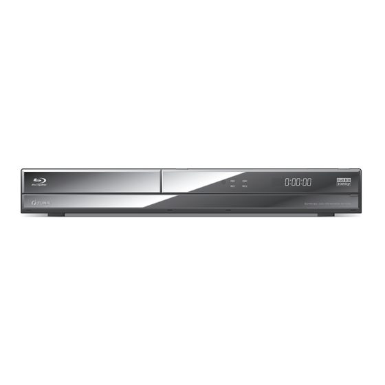
- Page 1 SERVICE MANUAL HDD & BLU-RAY DISC RECORDER BH2-M200...
-
Page 2: Table Of Contents
TABLE OF CONTENTS Specifications ................1-1-1 Laser Beam Safety Precautions . -
Page 3: Specifications
SPECIFICATIONS Specifications General Internal 3.5 inch HDD 500 GB Power requirements 220–240 V ± 10 %, 50 Hz ± 0.5 % Power consumption 34 W Power consumption (standby) 0.7 W Weight 4.0 kg Dimensions (width x height x depth) 430 x 61 x 315 mm Operating temperature 5°C to 40°C Operating humidity... -
Page 4: Laser Beam Safety Precautions
LASER BEAM SAFETY PRECAUTIONS This BD player uses a pickup that emits a laser beam. Do not look directly at the laser beam coming from the pickup or allow it to strike against your skin. The laser beam is emitted from the location shown in the figure. When checking the laser diode, be sure to keep your eyes at least 30 cm away from the pickup lens when the diode is turned on. -
Page 5: Important Safety Precautions
IMPORTANT SAFETY PRECAUTIONS Product Safety Notice K. When connecting or disconnecting the internal connectors, first, disconnect the AC plug from the Some electrical and mechanical parts have special AC outlet. safety-related characteristics which are often not L. When reassembling, be sure to use the original evident from visual inspection, nor can the protection screws or specified screws listed in the parts list. - Page 6 Safety Check after Servicing Examine the area surrounding the repaired location for damage or deterioration. Observe that screws, parts, and wires have been returned to their original positions. Afterwards, do the following tests and confirm the Chassis or Secondary Conductor specified values to verify compliance with safety standards.
-
Page 7: Standard Notes For Servicing
STANDARD NOTES FOR SERVICING Circuit Board Indications Pb (Lead) Free Solder 1. The output pin of the 3 pin Regulator ICs is When soldering, be sure to use the Pb free solder. indicated as shown. How to Remove / Install Flat Pack-IC Top View Bottom View 1. - Page 8 3. The flat pack-IC on the CBA is affixed with glue, so With Soldering Iron: be careful not to break or damage the foil of each 1. Using desoldering braid, remove the solder from pin or the solder lands under the IC when all pins of the flat pack-IC.
- Page 9 2. Installation With Iron Wire: 1. Using desoldering braid, remove the solder from 1. Using desoldering braid, remove the solder from all pins of the flat pack-IC. When you use solder the foil of each pin of the flat pack-IC on the CBA flux which is applied to all pins of the flat pack-IC, so you can install a replacement flat pack-IC more you can remove it easily.
- Page 10 Instructions for Handling Semi- conductors Electrostatic breakdown of the semi-conductors may occur due to a potential difference caused by electrostatic charge during unpacking or repair work. 1. Ground for Human Body Be sure to wear a grounding band (1 MΩ) that is properly grounded to remove any static electricity that may be charged on the body.
-
Page 11: Handling Precautions For Hdd
HANDLING PRECAUTIONS FOR HDD CAUTION: 4. OTHERS a. Be careful so as not to do the followings. 1. SHOCK Otherwise, HDD might be damaged. a. Exposing HDD to shock may be the biggest - DO NOT disassemble HDD. damaging factor. Please note that HDD is easily - When handling HDD, be sure to hold both sides damaged even if dropped from any height. -
Page 12: Cabinet Disassembly Instructions
CABINET DISASSEMBLY INSTRUCTIONS 1. Disassembly Flowchart Fig. Loc. Part Removal Note This flowchart indicates the disassembly steps to gain access to items to be serviced. When reassembling, BD/HDD 3(S-12), CN2804, follow the steps in reverse order. Bend, route, and [13] Main CBA CN7401, CN7402, dress the cables as they were originally. - Page 13 (S-3) (S-1) (S-1) [4] HDD Connector Assembly [1] Top Cover (S-1) SATA Cable Fig. D3 Fig. D1 [6] *HDD [5] HDD Bracket (S-4) Earth Plate CN2105 (L-1) (L-1) (S-2) HDD Damper (S-4) (S-2) HDD Damper Fig. D4 * See Reference Note 2. [3] Front CBA (L-2) (L-1)
- Page 14 [12] D-Tuner (S-5) CN502 (S-12) [13] *BD/HDD Main CBA Unit [7] BD Mechanism Assembly CN6101 CN7402 CN7401 CN5900 CN7100 Fig. D5 CN2804 Fig. D8 * See Reference Note 4. (S-6) [8] *Rear Panel (S-7) (S-8) (S-9) [14] Power (S-7) (S-13) (S-13) Supply CBA CN8002...
- Page 15 3. How to Eject a Disc When a disc cannot be removed due to malfunction or when an unplayable disc is inserted, follow the procedure below to remove the disc. Procedure A 1. Unplug the AC power cord and then plug it in. 2.
-
Page 16: How To Initialize The Hdd & Blu-Ray Disc Recorder
HOW TO INITIALIZE THE HDD & BLU-RAY DISC RECORDER To put the program back to the factory-default, initialize the unit by following the procedure below. 1. Turn the power on. 2. Put the unit into HDD/DISC mode. Remove the disc on the tray and close the tray. 3. -
Page 17: Firmware Renewal Mode
FIRMWARE RENEWAL MODE How to Prepare a Software Update 4. Select “Yes” to start firmware loading. Fig. c appears on the screen and Fig. d appears on the Disc (BE F/W, FE F/W) LCD. 1. Copy the “****.bin” file to a CD-R/RW or DVD-R/ RW disc. - Page 18 How to Confirm the Firmware Version 1. Turn the power on. 2. Put the unit into HDD/DISC mode. Remove the disc on the tray and close the tray. 3. Press [i] (skip up), [1], [2], [3] buttons on the remote control in this order. The following screen will be diplayed.
-
Page 19: Bd/Hdd Main Cba Unit Replacement
BD/HDD MAIN CBA UNIT REPLACEMENT When replacing the BD/HDD Main CBA Unit, the 6. Press [STANDBY/ON] button to turn the power off. board and HDD needs to be matched to one another. 7. Unplug the AC cord. Follow the procedure below to complete the matching process. -
Page 20: How To Format The Hdd After Replacement
HOW TO FORMAT THE HDD AFTER REPLACEMENT Note: HDD format is needed after replacing the HDD. 6. When format is completed, clock display appears Enter the Self Check Mode and complete HDD on the LCD. format by following the procedure below. Note: 1. -
Page 21: How To Display The Ld Operating Time
HOW TO DISPLAY THE LD OPERATING TIME 1. Turn the power on. 2. Put the unit into HDD/DISC mode. Remove the disc on the tray and close the tray. 3. Press [i] (skip up), [3], [2], [1] buttons on the remote control in this order. -
Page 22: Troubleshooting
TROUBLESHOOTING 1 Power Supply Section FLOW CHART NO.1 The power cannot be turned on. See FLOW CHART No.2 <The fuse blows out.> Is the fuse normal? Is normal state restored when once unplugged power Check for lead or short-circuiting of primary circuit cord is plugged again after several seconds. - Page 23 FLOW CHART NO.6 HDD+12V(FE+12V) is not outputted. Refer to "FLOW CHART NO.5"<EV+16V is not Is approximately +16V voltage supplied to Pin(2) of outputted>. IC1102? Check D1124, DRIVE-SW line and their periphery, Is approximately +5V voltage supplied to Pin(7) of and service it if defective. IC1102? Replace IC1102.
- Page 24 FLOW CHART NO.11 P-ON+5V(USB+5V, EV+5V-AV) is not outputted. (EV+5V is outputted normally.) Check Q2655, POWER-SW line and their periphery, Is approximately +4.5V voltage supplied to the base of and service it if defective. Q2605? Replace Q2605. FLOW CHART NO.12 EV+3.9V is not outputted. Refer to "FLOW CHART NO.8"<EV+5V(SYS+5V, Is approximately +5V voltage supplied to the collector LCD+5V) is not outputted>.
- Page 25 2 BD/HDD Section FLOW CHART NO.1 The key operation is not functioning. Are the contact point and the installation state Re-install the switches (SW3701-SW3707) correctly or of the key switches (SW3701-SW3707) normal? replace the poor switch. When pressing each switches (SW3701-SW3707), Check the switches (SW3701-SW3707) and their do the voltage of Pin(46, 47, 48, 55) of IC2701 periphery, and service it if detective.
- Page 26 FLOW CHART NO.5 VIDEO E-E does not appear normally. Are the video signals inputted to each pin of IC3004? Check the line between video input terminal and each pin of IC3004, and service it if defective. IC3004 17PIN VIDEO-IN 1 (AV1) →...
- Page 27 FLOW CHART NO.6 Picture does not appear normally. Set the disc on the disc tray, and playback it. (BD MODE) Or, playback by selecting the picture in HDD top menu. (HDD MODE) Are the video signals outputted to each pin of CN3001? Replace the BD Mechanism Assembly or BD/HDD Main CBA Unit.
- Page 28 FLOW CHART NO.7 Audio E-E does not appear normally. Check the line between audio input terminal and Are the audio signals inputted to each pin of IC3302? each pin of IC3302, and service it if defective. IC3302 2,15PIN AUDIO-IN1 (AV1) →...
- Page 29 FLOW CHART NO.8 Audio is not outputted during playback. Set the disc on the disc tray, and playback it. (DVD MODE) Or, playback by selecting the picture in HDD top menu. (HDD MODE) Replace the BD Mechanism Assembly or BD/HDD Are the analog audio signals outputted to each pin of Main CBA Unit.
-
Page 30: Error Display On The Front Panel
ERROR DISPLAY ON THE FRONT PANEL If malfunction occurs in the power supply, safety detection (IC2701) on the Power Supply Board is activated the next time power is turned on, and error will be displayed on the front panel. When an error is displayed, check whether the monitoring parts on the power line is defective. Replace the defective part(s) which is causing malfunction. -
Page 31: Block Diagrams
BLOCK DIAGRAMS System Control Block Diagram ....E4V21BLS 1-14-1... - Page 32 Digital Signal Process Block Diagram E4V21BLD 1-14-2...
- Page 33 Video Block Diagram E4V21BLV 1-14-3...
- Page 34 Audio Block Diagram E4V21BLA 1-14-4...
- Page 35 Power Supply Block Diagram E4V21BLP 1-14-5...
-
Page 36: Schematic Diagrams / Cba And Test Points
SCHEMATIC DIAGRAMS / CBA AND TEST POINTS Standard Notes WARNING Many electrical and mechanical parts in this chassis have special characteristics. These characteristics often pass unnoticed and the protection afforded by them cannot necessarily be obtained by using replacement components rated for higher voltage, wattage, etc. - Page 37 LIST OF CAUTION, NOTES, AND SYMBOLS USED IN THE SCHEMATIC DIAGRAMS ON THE FOLLOWING PAGES: 1. CAUTION: FOR CONTINUED PROTECTION AGAINST FIRE HAZARD, REPLACE ONLY WITH THE SAME TYPE FUSE. 2. CAUTION: Fixed Voltage (or Auto voltage selectable) power supply circuit is used in this unit. If Main Fuse (F1001) is blown, first check to see that all components in the power supply circuit are not defective before you connect the AC plug to the AC power supply.
- Page 38 Power Supply 1 Schematic Diagram CAUTION ! 1 NOTE: CAUTION ! NOTE: For continued protection against fire hazard, When you replace Diodes (D1101,D1116,D1117) on the Power Supply CBA, Fixed voltage (or Auto voltage selectable) power supply circuit is used in this unit. The voltage for parts in hot circuit is measured using replace only with the same type fuse.
- Page 39 Power Supply 2 Schematic Diagram TO BD/HDD MAIN CN2104 CBA UNIT CN7401 1 FAN 2 NU 3 BD/HDD-AUDIO-MUTE Q2702 2SA1267Y 4 GND (P-DOWN DET) 5 DT-SAFETY 6 DT-REG-CONT D2701 D2702 R2705 7 GND WIRE 100K 4V3BSB R2704 R2737 47K -T26 8 1V2CONT 6.8K 9 1V8CONT...
- Page 40 Power Supply 3 Schematic Diagram POWER SUPPLY CBA TO BD/HDD MAIN CN2802 CBA UNIT CN7402 R2805 CN2101 (BD MECHANISM) DATA1 1 DRIVE-SAFETY R2806 2 FE+5V DATA0 C2809 C2807 3 GND GND 8 R2807 4 GND SCLK 7 12.1 5 FE+12V GND 6 R2808 C2810...
- Page 41 Front Schematic Diagram V3001 MATRIX CHART COM1 COM2 COM3 COM4 SG10 SG11 SG12 COL1 SG13 SG14 V3001 DP-0027-001-NR-KK (LCD MODULE) SG15 SG16 SG17 R3714 R3713 R3710 R3709 SG18 COL1 COL2 SG19 D3704 D3703 D3701 D3702 31 32 LTL-1CHEE LTL-1CHEE LTL1CHCBK2-F LTL1CHCBK2-F SG20 COL2...
- Page 42 Scart Schematic Diagram R3904 R3908 SCART CBA R3902 100K R3906 3.3K -2.3 Q3902 MMBTSC3875Y (MUTE) R3903 R3907 JK3501 AV2(DECODER) R3901 100K R3905 3.3K TO JACK CBA -2.3 CN3501 CN3003 Q3901 AUDIO(R)-OUT2 MMBTSC3875Y Z3901 Z3802 Z3902 (MUTE) AUDIO-MUTE2 VARISTOR VARISTOR VARISTOR R3804 AUDIO(L)-OUT2 R3802...
- Page 43 Jack Schematic Diagram JACK CBA R3030 C3034 C3032 47/16V JK3002(REAR) AV1(TV) C3020 C3035 C3040 C3057 C3058 C3021 C3059 47/16V 12.0 R3416 R3418 R3420 C3414 Q3453 R3415 100K 1000P 20 19 18 17 MMBTSA1504Y (MUTE DRIVE) -2.3 R3417 R3419 C3413 -2.3 100K 1000P R3422...
- Page 44 D-Tuner Schematic Diagram TU8001 (TUNER UNIT) D-TUNER CBA ANT-IN ANT-OUT 10 11 13 14 15 16 17 18 19 C8061 C8062 C8066 C8064 R8070 BEAD C8065 IC8011 PQ070XNA1ZPH R8036 (+3.3V REG.) 5.2 5.2 3.4 1.3 D8011 R8015 C8014 C8013 1SS400ST C8015 R8013 R8011...
- Page 45 BD/HDD Main 1 Schematic Diagram 2 NOTE: The order of pins shown in this diagram is different from that of actual IC6001. IC6001 is divided into nine and shown as IC6001 (1/9) ~ IC6001 (9/9) in this BD/HDD Main Schematic Diagram Section. CONTINUE BD/HDD MAIN 11 PCA-DATA...
- Page 46 BD/HDD Main 2 Schematic Diagram 2 NOTE: The order of pins shown in this diagram is different from that of actual IC6001. IC6001 is divided into nine and shown as IC6001 (1/9) ~ IC6001 (9/9) in this BD/HDD Main Schematic Diagram Section. BD/HDD MAIN CBA UNIT CONTINUE BD/HDD MAIN 9...
- Page 47 BD/HDD Main 3 Schematic Diagram 2 NOTE: The order of pins shown in this diagram is different from that of actual IC6001. IC6001 is divided into nine and shown as IC6001 (1/9) ~ IC6001 (9/9) in this BD/HDD Main Schematic Diagram Section. BD/HDD MAIN CBA UNIT CONTINUE BD/HDD MAIN 2...
- Page 48 BD/HDD Main 4 Schematic Diagram 2 NOTE: The order of pins shown in this diagram is different from that of actual IC6001. IC6001 is divided into nine and shown as IC6001 (1/9) ~ IC6001 (9/9) in this BD/HDD Main Schematic Diagram Section. BD/HDD MAIN CBA UNIT IC6001(4/9) MN2WS0038DP2-B...
- Page 49 BD/HDD Main 5 Schematic Diagram 2 NOTE: The order of pins shown in this diagram is different from that of actual IC6001. IC6001 is divided into nine and shown as IC6001 (1/9) ~ IC6001 (9/9) in this BD/HDD Main Schematic Diagram Section. BD/HDD MAIN CBA UNIT IC6001(5/9) MN2WS0038DP2-B...
- Page 50 BD/HDD Main 6 Schematic Diagram 2 NOTE: The order of pins shown in this diagram is different from that of actual IC6001. IC6001 is divided into nine and shown as IC6001 (1/9) ~ IC6001 (9/9) in this BD/HDD Main Schematic Diagram Section. BD/HDD MAIN CBA UNIT CONTINUE IC6001(6/9)
- Page 51 BD/HDD Main 7 Schematic Diagram 2 NOTE: The order of pins shown in this diagram is different from that of actual IC6001. IC6001 is divided into nine and shown as IC6001 (1/9) ~ IC6001 (9/9) in this BD/HDD Main Schematic Diagram Section. CONTINUE BD/HDD MAIN 9 P-ON+3.3V...
- Page 52 BD/HDD Main 8 Schematic Diagram 2 NOTE: The order of pins shown in this diagram is different from that of actual IC6001. IC6001 is divided into nine and shown as IC6001 (1/9) ~ IC6001 (9/9) in this BD/HDD Main Schematic Diagram Section. CONTINUE BD/HDD MAIN 9 P-ON+3.3V...
- Page 53 BD/HDD Main 9 Schematic Diagram 2 NOTE: The order of pins shown in this diagram is different from that of actual IC6001. IC6001 is divided into nine and shown as IC6001 (1/9) ~ IC6001 (9/9) in this BD/HDD Main Schematic Diagram Section. CONTINUE BD/HDD MAIN 2 P-ON+3.3V...
- Page 54 BD/HDD Main 10 Schematic Diagram CONTINUE BD/HDD MAIN 7 PRMVS BD/HDD MAIN CBA UNIT PRMHS PRMCLK CONTINUE CONTINUE BD/HDD MAIN 7 BD/HDD MAIN 8 PRMC(0-11) SCL3 PRMY(0-11) SDA3 CONTINUE BD/HDD MAIN 9 P-ON+3.3V P-ON+1.2V C5217 C5218 C5219 R5293 P-ON+5V C5200 C5221 C5222 R5294...
- Page 55 BD/HDD Main 11 Schematic Diagram BD/HDD MAIN CBA UNIT Q5602 MMBTSA1981Y (+1.5V REG.) C5633 C5615 R5662 R5690 X5601 R5664 25MHz CONTINUE CONTINUE BD/HDD MAIN 1 BD/HDD MAIN 9 PCA-DATA P-ON+3.3V [0-31] C5690 C5691 R5600 PCAD0 R5635 2.49K R5601 PCAD1 IC5601 RTL8140L-GR 124 123 120 119 118 117 116 115 114 113 112 111 110 109 108 107 106 105 104 103...
- Page 56 Power Supply CBA, Front CBA & Scart CBA Top View NOTE: Because a hot chassis ground is present in the power supply CAUTION ! circuit, an isolation transformer must be used when repairing. The voltage for parts in hot circuit is measured using Fixed voltage (or Auto voltage selectable) power supply circuit is used in this unit.
- Page 57 Power Supply CBA, Front CBA & Scart CBA Bottom View CAUTION ! Because a hot chassis ground is present in the power supply NOTE: Fixed voltage (or Auto voltage selectable) power supply circuit is used in this unit. circuit, an isolation transformer must be used when repairing. The voltage for parts in hot circuit is measured using If Main Fuse (F1001) is blown , check to see that all components in the power supply Also, in order to have the ability to increase the input slowly,...
- Page 58 Jack CBA Top View Jack CBA Bottom View Z3002 C3076 Z3006 Z3007 R3101 JK3002 PIN 27 OF C3415 R3411 JK3003 L3008 CN3001 D3012 Z3008 Z3001 D3012 Z3003 C3087 C3414 Z3004 Z3005 R3417 R3412 R3417 Q3402 JK3001 Q3452 R3212 R3212 PIN 19 OF Q3404 L3002 R3420...
- Page 59 D- Tuner CBA Top View IC8021 R8025 IC8031 BE4V20F0205 C8023 C8051 C8072 R8051 L8051 C8070 C8052 CN8002 R8052 L8052 C8073 R8053 L8053 C8022 R8054 L8054 C8053 C8066 C8054 TU8001 R8022 R8024 R8021 C8032 IC8041 C8061 C8063 R8059 R8060 C8015 D8011 C8011 R8072 R8014...
-
Page 60: Waveforms
WAVEFORMS Pin 6 of CN3001 Pin 15 of CN3001 VIDEO-Pr/Cr VIDEO-Pr/Cr 0.2V 0.2V 20µsec VIDEO-OUT VIDEO-OUT 0.5V 0.5V 20µsec Pin 19 of CN3001 Pin 4 of CN3001 AUDIO(L)-OUT AUDIO(L)-OUT 0.5ms 0.5ms VIDEO-Y VIDEO-Y 0.2V 0.2V 20µsec Pin 27 of CN3001 Pin 2 of CN3001 SPDIF SPDIF... -
Page 61: Wiring Diagram
WIRING DIAGRAM E4V21WI 1-17-1... -
Page 62: Ic Pin Function Descriptions
IC PIN FUNCTION DESCRIPTIONS IC2701 ( SUB MICRO CONTROLLER ) Signal Function Name Signal Function Name Not Used Ground Not Used IN VREF +5V Power Supply Not Used IN MODE Not Used Not Used IN XCIN Sub Clock Input IN REMOTE Remote Signal Input 5 OUT XCOUT Sub Clock Output... - Page 63 IC3701 ( LCD DRIVER ) Signal Function Name SG17 SG18 SG19 SG20 SG21 SG22 SG23 SG24 SG25 SG26 SG27 SG28 SG16 SG15 Segment Output Serial Data Input SG14 SG13 SG12 SG11 SG10 Not Used Not Used Not Used Not Used Not Used 34 OUT COM4 Common Terminal 4...
-
Page 64: Lead Identifications
LEAD IDENTIFICATIONS 2SA1981Y-AT STD1862Y-AT KIA431-AT/P 2SA1267Y 2SC3199Y E C B E C B E C B R A K MMBTRC102SS BD9321EFJ-E2 PQ035NZ01ZPH MMBTRC103SS FA5640N PQ070XNA1ZPH MMBTSC3875G UTC4580TE PS2561A-1-V-A(W) MMBTSC3875Y MMBTSA1504Y 3 1: Anode 2: Cathode 3: Emitter 4: Collector LV7109E-MPB-E 2SK3566(Q M) 4052L-S16-R G D S... -
Page 65: Exploded Views
EXPLODED VIEWS Cabinet 2L010 2L010 Scart CBA 2L042 B-24 Jack CBA 2L050 2L045 2L070 2L045 2L070 D-Tuner CBA 2L010 2B26 2L041 2L020 2L011 2B22 2L014 2L070 2L012 2B22 2L041 BD/HDD Main CBA Unit 2B12 2L022 2B39 2B41 2L011 2L040 2L040 AC1001 FM1001 F1001... - Page 66 Packing X20-A X20-B X20-C X20-D Lower Side Upper Side X1-1 Some Ref. Numbers are not in sequence. 1-20-2 E4V21PEX...
-
Page 67: Mechanical Parts List
MECHANICAL PARTS LIST PRODUCT SAFETY NOTE: Products marked with a Ref. No. Description Part No. ! have special characteristics important to safety. ACCESSORIES Before replacing any of these components, read X1-1 REMOTE CONTROL UNIT NC119ED NC119ED carefully the product safety notice in this service MANGANESE DRY BATTERY R6UWC/2STA or XB0M311MS003 manual. -
Page 68: Electrical Parts List
ELECTRICAL PARTS LIST PRODUCT SAFETY NOTE: Products marked with a Ref. No. Description Part No. ! have special characteristics important to safety. METALIZED FILM CAP . 0.047µF/250V M CT2E473MS037 Before replacing any of these components, read C1012! CAP CERAMIC 3300pF/250V/M or CA2E332MR086 carefully the product safety notice in this service SAFTY CAP . - Page 69 Ref. No. Description Part No. Ref. No. Description Part No. C1129 CHIP CERAMIC CAP .(1608) B K 1000pF/50V or CHD1JK30B102 CHIP CERAMIC CAP .(1608) Y5V/Z/0.1µF/25V CHD1040YF098 CHIP CERAMIC CAP .(1608) X7R/K/1000pF/50V CHD1020YF069 C2611 CHIP CERAMIC CAP .(2125) B K 4.7µF/25V or CA1E475MR084 C1130 CHIP CERAMIC CAP .
- Page 70 Ref. No. Description Part No. Ref. No. Description Part No. FMN CONNECTOR TOP 10P 10FMN-BTRK- JCFNG10JG020 DIODE SWITCHING HSS4148TE-E QDTZ0HSS4148 A(LF)(SN) D1111 DIODE SWITCHING 1N4148-F0021 or NDTZ01N4148F CN2107 CONNECTOR 6PIN(TOP) A2001WV-6P-Y J3A206JSY001 SWITCHING DIODE 1SS133(T-77) or QDTZ001SS133 CN2802 WIRE ASSEMBLY POWER-MAIN 14PINFFC WX1E4V20-003 DIODE SWITCHING HSS4148TE-E QDTZ0HSS4148...
- Page 71 Ref. No. Description Part No. Ref. No. Description Part No. D1116 SCHOTTKY BARRIER DIODE SMD SK59 ND1Z000SK59S PNP TRANSISTOR 2SA1980M Y or NQSY2SA1980M D1117 SCHOTTKY BARRIER DIODE SMD SK59 ND1Z000SK59S TRANSISTOR KTA1267-Y -AT/P or NQSYKTA1267P PNP TRANSISTOR 2SA1980MG-AT or NQSG2SA1980M TRANSISTOR KTA1267-GR-AT/P NQS1KTA1267P IC1001...
- Page 72 Ref. No. Description Part No. Ref. No. Description Part No. CHIP RES. 1/10W J 10 Ω or TRANSISTOR SRC1203SF or NQ1ZSRC1203S R1008 RRXAJR5Z0100 RES CHIP 1608 1/10W J 10 Ω TRANSISTOR KRC103S-RTK/P NQ1ZKRC103SP RRXA100YF002 CHIP RES. 1/10W J 4.7k Ω or Q2701 NPN TRANSISTOR ST 2SC3199Y or NQSYT2SC3199...
- Page 73 Ref. No. Description Part No. Ref. No. Description Part No. CHIP RES.(1608) 1/10W 0 Ω or CHIP RES. 1/10W J 1k Ω or R1122 RRXAZR5Z0000 R1175 RRXAJR5Z0102 RES CHIP 1608 1/10W J 0 Ω RES CHIP 1608 1/10W J 1.0k Ω RRXA000YF002 RRXA102YF002 CHIP RES.
- Page 74 Ref. No. Description Part No. Ref. No. Description Part No. RES CHIP 1608 1/10W J 220k Ω CHIP RES. 1/10W J 4.7k Ω or RRXA224YF002 R2763 RRXAJR5Z0472 CHIP RES. 1/10W J 100k Ω or RES CHIP 1608 1/10W J 4.7k Ω R2715 RRXAJR5Z0104 RRXA472YF002...
- Page 75 Ref. No. Description Part No. Ref. No. Description Part No. CHIP RES. 1/10W J 360 Ω or JP1108 WIRE CP STP-S-0.60 or XZ40F0REN002 R3704 RRXAJR5Z0361 RES CHIP 1608 1/10W J 360 Ω WIRE CP CP0.56 XZ40F0XRC001 RRXA361YF002 CHIP RES. 1/10W J 620 Ω or JP1110 WIRE CP STP-S-0.60 or XZ40F0REN002...
- Page 76 Ref. No. Description Part No. Ref. No. Description Part No. RES CARBON FILM 1/4W J 220 Ω CONNECTOR RCJ221PAK001 CARBON RES. 1/4W J 220 Ω or R3804 RCX4JATZ0221 CN3501 CONNECTOR PRINT OSU S15B-PH-K- J3PHC15JG030 S(LF)(SN) RES CARBON FILM 1/4W J 220 Ω RCJ221PAK001 DIODES CHIP RES.
- Page 77 Ref. No. Description Part No. Ref. No. Description Part No. CHIP CERAMIC CAP .(1608) Y5V/Z/0.1µF/25V CHD1040YF098 CAP ELECTROLYTIC 10µF/16V/M or CA1C100ENE12 C3041 ELECTROLYTIC CAP . 22µF/16V M or CEC22RENW016 ELECTROLYTIC CAP . 10µF/16V M CE1CMASDL100 CAP ELECTROLYTIC 22µF/16V/M or CA1C220ENE12 C3302 ELECTROLYTIC CAP .
- Page 78 Ref. No. Description Part No. Ref. No. Description Part No. CAP ELECTROLYTIC 10µF/16V/M or CA1C100ENE12 ELECTROLYTIC CAP . 10µF/16V M CE1CMASDL100 IC3004 IC AV SWITCH LV7109E-MPB-E QSCA0R0SY005 C3413 CHIP CERAMIC CAP .(1608) CH J 1000pF/50V CHD1JJ3CH102 IC3301 IC OP AMP UTC4580TE or NSCA0T02H001 IC OP AMP UTC4580E or NSZBA0T2H010...
- Page 79 Ref. No. Description Part No. Ref. No. Description Part No. CARBON RES. 1/4W J 75 Ω or Q3451 PNP TRANSISTOR SMD MMBTSA1504Y or NQ1YBTSA1504 R3212 RCX4JATZ0750 RES CARBON FILM 1/4W J 75 Ω PNP TRANSISTOR SMD 2SA1980SFY or NQ1Y2SA1980S RCJ750PAK001 CHIP RES.
- Page 80 Ref. No. Description Part No. Ref. No. Description Part No. RES CHIP 1608 1/10W J 10k Ω CHIP RES. 1/10W J 220 Ω or RRXA103YF002 R3458 RRXAJR5Z0221 CHIP RES. 1/10W J 33k Ω or RES CHIP 1608 1/10W J 220 Ω R3354 RRXAJR5Z0333 RRXA221YF002...
- Page 81 Ref. No. Description Part No. Ref. No. Description Part No. C8054 CHIP CERAMIC CAP .(1608) CH J 22pF/50V or CHD1JJ3CH220 CHIP INDUCTOR BK1608LL300-T LLF3000TU008 CHIP CERAMIC CAP .(1608) NP0/J/22pF/50V CHD2200YF020 L8056 MULTI_LAYER CHIP FERRITE BEADS LLEC03SSN004 SZ1608G300TF or C8055 CHIP CERAMIC CAP .(1608) CH J 22pF/50V or CHD1JJ3CH220 CHIP INDUCTOR BK1608LL300-T LLF3000TU008...
- Page 82 BH2-M200 E4V21ED 2011-04-22 Ver.1...
Need help?
Do you have a question about the BH2-M200 and is the answer not in the manual?
Questions and answers