Table of Contents
Advertisement
Advertisement
Table of Contents

Related Manuals for Clevo W370ST


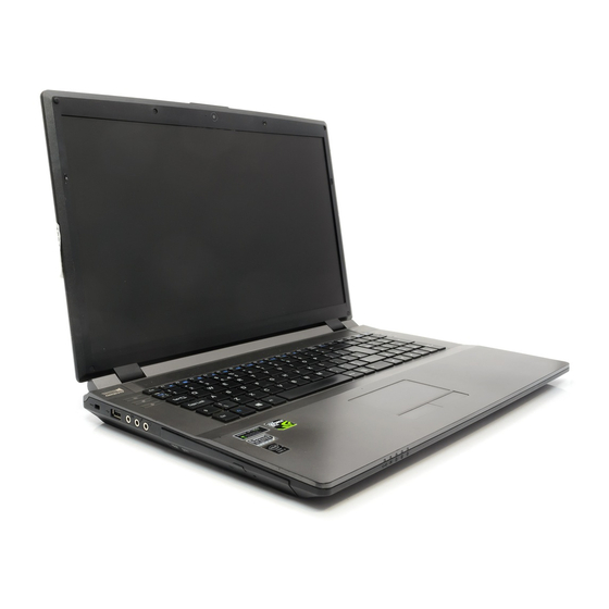
Summary of Contents for Clevo W370ST
- Page 1 W370ST...
- Page 3 Preface Notebook Computer W370ST Service Manual...
- Page 4 Preface Notice The company reserves the right to revise this publication or to change its contents without notice. Information contained herein is for reference only and does not constitute a commitment on the part of the manufacturer or any subsequent ven- dor.
- Page 5 This manual is intended for service personnel who have completed sufficient training to undertake the maintenance and inspection of personal computers. It is organized to allow you to look up basic information for servicing and/or upgrading components of the W370ST se- ries notebook PC.
- Page 6 Preface IMPORTANT SAFETY INSTRUCTIONS Follow basic safety precautions, including those listed below, to reduce the risk of fire, electric shock and injury to per- sons when using any electrical equipment: 1. Do not use this product near water, for example near a bath tub, wash bowl, kitchen sink or laundry tub, in a wet basement or near a swimming pool.
-
Page 7: Instructions For Care And Operation
Preface Instructions for Care and Operation The notebook computer is quite rugged, but it can be damaged. To prevent this, follow these suggestions: Don’t drop it, or expose it to shock. If the computer falls, the case and the components could be damaged. Do not expose the computer Do not place it on an unstable Do not place anything heavy... -
Page 8: Power Safety
Preface Avoid interference. Keep the computer away from high capacity transformers, electric motors, and other strong mag- netic fields. These can hinder proper performance and damage your data. Take care when using peripheral devices. Use only approved brands of Unplug the power cord before peripherals. -
Page 9: Battery Precautions
Preface Battery Precautions • Only use batteries designed for this computer. The wrong battery type may explode, leak or damage the computer. • Do not continue to use a battery that has been dropped, or that appears damaged (e.g. bent or twisted) in any way. Even if the computer continues to work with a damaged battery in place, it may cause circuit damage, which may possibly result in fire. - Page 10 Preface Related Documents You may also need to consult the following manual for additional information: User’s Manual on CD This describes the notebook PC’s features and the procedures for operating the computer and its ROM-based setup pro- gram. It also describes the installation and operation of the utility programs provided with the notebook PC. VIII...
-
Page 11: Table Of Contents
Preface Contents Introduction ..........1-1 2nd HDD ..................A-7 DVD ....................A-8 Overview ..................1-1 COMBO ..................A-9 System Specifications ..............1-2 Schematic Diagrams......... B-1 External Locator - Front View with LCD Panel Open ....1-4 External Locator - Front & Right side Views .........1-5 System Block Diagram ..............B-2 External Locator - Left Side &... - Page 12 W370/350STQ Click Board ............B-50 W370ST Power Switch Board ............. B-51 W350STQ Power Switch Board ..........B-52 W370ST LID / VGA LED Board ..........B-53 W350STQ LID / VGA LED Board ..........B-54 W350STQ VGA / WLAN SW Board .......... B-55 POWER ON SEQUENCE ............
-
Page 13: Introduction
Chapter 1: Introduction Overview This manual covers the information you need to service or upgrade the W370ST series notebook computer. Information about operating the computer (e.g. getting started, and the Setup utility) is in the User’s Manual. Information about driv- ers (e.g. -
Page 14: System Specifications
Introduction System Specifications Security Interface Processor Options BIOS Password One USB 2.0 Port Intel® Core™ i7 Processor Security (Kensington® Type) Lock Slot Three USB 3.0 Ports i7-4900MQ (2.80GHz) (Factory Option) Fingerprint Reader (Model A One eSATA Port (USB 3.0 Port Combined) 8MB L3 Cache, 22nm, DDR3L-1600MHz, TDP Only) One HDMI-Out Port... - Page 15 Introduction Communication Built-In Gigabit Ethernet LAN (Factory Option) 2M HD PC Camera Module WLAN/ Bluetooth Half Mini-Card Modules: (Factory Option) Intel® Centrino® Advanced-N 6235 Wireless LAN (802.11a/g/n) + Bluetooth (Factory Option) Intel® Centrino® Wireless-N 2230 Wireless LAN (802.11b/g/n)+ Bluetooth 4.0 (Factory Option) Third-Party Wireless LAN (802.11b/g/n) (Factory Option) Third-Party Wireless LAN...
-
Page 16: External Locator - Front View With Lcd Panel Open
Introduction External Locator - Front View with LCD Panel Open Figure 1 Top View 1. Built-In PC Camera (Optional) 2. PC Camera LED 3. LCD 4. Power Button 5. GPU Button 6. Speakers 7. Top Case LED Indicators 8. Hot Key Buttons 9. -
Page 17: External Locator - Front & Right Side Views
Introduction External Locator - Front & Right side Views Figure 2 Front Views 1. LED Indicators Figure 3 Right Side Views 1. Multi-in-1 Card Reader 2. USB 3.0 Ports 3. Combined eSATA/ USB 3.0 Port 4. HDMI-Out Port 5. RJ-45 LAN Jack External Locator - Front &... -
Page 18: External Locator - Left Side & Rear View
Introduction External Locator - Left Side & Rear View Figure 4 Left Side View 1. Security Lock Slot 2. USB 2.0 Port 3. S/PDIF-Out Jack 4. Microphone-In Jack 5. Headphone-Out Jack 6. Optical Device Drive 7. Emergency Eject Hole Figure 5 Rear View 1. -
Page 19: External Locator - Bottom View
Introduction External Locator - Bottom View Figure 6 Bottom View 1. Component Bay Cover 2. Vent 3. Battery 4. HDD Bay Overheating To prevent your com- puter from overheating make sure nothing blocks the vent/fan in- takes while the com- puter is in use. -
Page 20: Mainboard Overview - Top (Key Parts)
Introduction Mainboard Overview - Top (Key Parts) Figure 7 Mainboard Top Key Parts 1. Memory Slots DDR3L So-DIMM 2. CMOS Battery 3. Mini-Card Connector (3G Module) 4. Mini-Card Connector (WLAN Module) 1 - 8 Mainboard Overview - Top (Key Parts) -
Page 21: Mainboard Overview - Bottom (Key Parts)
Introduction Mainboard Overview - Bottom (Key Parts) Figure 8 Mainboard Bottom Key Parts 1. PantherPoint Controller 2. CPU Socket 3. Memory Slots DDR3L So-DIMM 4. NV Graphic 5. KBC Mainboard Overview - Bottom (Key Parts) 1 - 9... -
Page 22: Mainboard Overview - Top (Connectors)
Introduction Mainboard Overview - Top (Connectors) Figure 9 Mainboard Top Connectors 1. Audio Cable Connector 2. Power Switch Cable Connector 3. ODD Cable Connector 4. Keyboard Cable Connector 5. Click Board Cable Connector 6. VGA SW Cable Connector 7. Speaker Cable Connector 8. -
Page 23: Mainboard Overview - Bottom (Connectors)
Introduction Mainboard Overview - Bottom (Connectors) Figure 10 Mainboard Bottom Connectors 1. HDD2 Connector 2. External Monitor Port 3. DC-In Jack 4. Fan Cable Connector 5. CCD Cable Connector 6. HDD1 Connector 7. Battery Connector 8. LCD Cable Connector Mainboard Overview - Bottom (Connectors) 1 - 11... - Page 24 Introduction 1 - 12...
-
Page 25: Disassembly
Chapter 2: Disassembly Overview This chapter provides step-by-step instructions for disassembling the W370ST series notebook’s parts and subsystems. When it comes to reassembly, reverse the procedures (unless otherwise indicated). We suggest you completely review any procedure before you take the computer apart. -
Page 26: Maintenance Tools
Disassembly NOTE: All disassembly procedures assume that the system is turned OFF, and disconnected from any power supply (the battery is removed too). Maintenance Tools The following tools are recommended when working on the notebook PC: • M3 Philips-head screwdriver •... -
Page 27: Maintenance Precautions
Disassembly Maintenance Precautions The following precautions are a reminder. To avoid personal injury or damage to the computer while performing a re- moval and/or replacement job, take the following precautions: Power Safety Warning 1. Don't drop it. Perform your repairs and/or upgrades on a stable surface. If the computer falls, the case and other Before you undertake components could be damaged. -
Page 28: Disassembly Steps
Disassembly Disassembly Steps The following table lists the disassembly steps, and on which page to find the related information. PLEASE PERFORM THE DISASSEMBLY STEPS IN THE ORDER INDICATED. To remove the Battery: 1. Remove the battery page 2 - 5 To remove the Optical Device: 1. -
Page 29: Removing The Battery
Disassembly Removing the Battery Figure 1 Battery Removal If you are confident in undertaking upgrade procedures yourself, for safety reasons it is best to remove the battery. a. Slide the latch in the 1. Turn the computer off, and turn it over. direction of the arrow. -
Page 30: Removing The Optical (Cd/Dvd) Device
Disassembly Removing the Optical (CD/DVD) Device Figure 2 Optical Device 1. Turn off the computer, and turn it over and remove the battery (page 2 - 5) and remove the component bay cover Removal (page 2 - 2. Remove the screw , and use a screwdriver to carefully push out the optical device at point a. -
Page 31: Removing The Hard Disk Drive
Disassembly Removing the Hard Disk Drive Figure 3 The hard disk drive is mounted in a removable case and can be taken out to accommodate other 2.5" SATA hard disk HDD Assembly drives with a height of 9.5mm or 7mm (h). Follow your operating system’s installation instructions, and install all nec- Removal essary drivers and utilities (as outlined in Chapter 4 of the User’s Manual) when setting up a new hard disk. - Page 32 Disassembly 5. Lift the hard disk assembly out of the computer (Figure 4c Figure 4 6. Remove screws HDD Assembly 7. Separate the hard disk and hard disk mylar Removal (cont’d.) 8. Reverse the process to install a new hard disk(s). c.
- Page 33 Disassembly Hard Disk Size Note (Foam Rubber Insert) Note that the hard disks pictured on the following pages are all 9.5mm(H) hard disk drives. In some cases 7mm(H) hard disk drives will be installed. For more information contact your distributor/supplier, and bear in mind your warranty terms.
- Page 34 Disassembly Removing the Hard Disk(s) in the Secondary HDD Bay Figure 6 1. Turn off the computer, and turn it over and remove the battery. Secondary HDD 2. Locate the component bay cover and remove screws and the cover. Assembly Removal 3.
-
Page 35: Removing And Installing The Processor
Disassembly Removing and Installing the Processor Figure 7 Processor Removal Processor Removal Procedure 1. Turn off the computer, and turn it over, remove the battery (page 2 - 5), and component bay cover (page 2 - 10). a. Locate the heat sink. 2. - Page 36 Disassembly 5. Turn the release latch towards the unlock symbol to release the CPU (Figure 8d). Figure 8 6. Carefully (it may be hot) lift the CPU up and out of the socket (Figure 8e). Processor Removal 7. Reverse the process to install a new CPU. (cont’d) 8.
- Page 37 Disassembly Processor Installation Procedure Figure 9 Processor 1. Insert the CPU (Figure 9a), pay careful attention to the pin alignment, it will fit only one way (DO NOT FORCE Installation IT!), and turn the release latch towards the lock symbol (Figure 9b).
-
Page 38: Removing The Keyboard
Disassembly Removing the Keyboard Figure 10 Keyboard Removal 1. Turn off the computer, and turn it over and remove the battery (page 2 - 5), and component bay cover (page 2 - 10). a. Use a screwdriver to 2. Use a screwdriver to carefully push out the speakers cover at point carefully push out the 3. -
Page 39: Removing The Primary System Memory (Ram)
Disassembly Removing the Primary System Memory (RAM) Figure 11 Primary RAM The computer has three memory sockets for 204 pin Small Outline Dual In-line (SO-DIMM) DDR III (DDR3L) type mem- Module Removal ory modules. The total memory size is automatically detected by the POST routine once you turn on your computer. a. - Page 40 Disassembly Memory (under Keyboard) Upgrade Process Figure 12 RAM Module 5. Turn off the computer, turn it over and remove the battery (page 2 - 5), component bay cover (page 2 - 10) and (under keyboard) keyboard (page 2 - 14).
-
Page 41: Part Lists
Part Lists Appendix A: Part Lists This appendix breaks down the W370ST series notebook’s construction into a series of illustrations. The component part numbers are indicated in the tables opposite the drawings. Note: This section indicates the manufacturer’s part numbers. Your organization may use a different system, so be sure to cross-check any relevant documentation. -
Page 42: Part List Illustration Location
Part Lists Part List Illustration Location The following table indicates where to find the appropriate part list illustration. Table A- 1 Part List Illustration Location Parts page A - 3 Bottom page A - 4 page A - 5 page A - 6 2nd HDD page A - 7 page A - 8... -
Page 43: Top
Part Lists Figure A - 1 Top A - 3... -
Page 44: Bottom
Part Lists Bottom Figure A - 2 Bottom A - 4 Bottom... -
Page 45: Lcd
Part Lists Figure A - 3 LCD A - 5... -
Page 46: Hdd
Part Lists Figure A - 4 A - 6 HDD... -
Page 47: 2Nd Hdd
Part Lists 2nd HDD Figure A - 5 2nd HDD 2nd HDD A - 7... -
Page 48: Dvd
Part Lists Figure A - 6 A - 8 DVD... -
Page 49: Combo
Part Lists COMBO Figure A - 7 COMBO COMBO A - 9... - Page 50 Part Lists A - 10...
-
Page 51: Schematic Diagrams
W370/350STQ Click Board - Page B - 50 Version Note PS8625 - Page B - 13 USB Charge, CCD, TPM, Multi-Con - Page B - 33 W370ST Power Switch Board - Page B - 51 schematic dia- Panel, Inverter, CRT - Page B - 14... - Page 52 Schematic Diagrams System Block Diagram W3X0ST System Block Diagram 5V,3V,5VS,3VS,3.3VM SHEET 39 Haswell 3 vias <6" PCIe*8 PS8625 2 vias <7" 2" ~ 6" PROCESSOR (EDP TO LVDS) 1.05V_LAN_M,1.05V_M SHEET 42 SHEET 12 1.05VS rPGA946B Nvidia DDR3 /1.35 37.5x37.5mm 1067/1333/1600 MHz Fermi N14x VDD3,VDD5,FBVDDQ DDRIII...
- Page 53 Schematic Diagrams Haswell 1/7 Haswell rPGA Processor 1/7 ( DMI,PEG,FDI ) +VCCIOA_OUT U15A Haswell rPGA EDS CPU HOLD PEG_IRCOMP 24.9_1%_04 PEG_RCOMP PEG_RX#0 PEG_RXN_0 DMI_RXN_0 PEG_RXN_1 PEG_RX#1 DMI_TXN0 DMI_TXN1 DMI_RXN_1 PEG_RXN_2 PEG_RX#2 H8_0D4_3 H8_0D4_3 H8_0D4_3 H8_0D4_3 PEG_RX#3 DMI_TXN2 DMI_RXN_2 PEG_RXN_3 Sheet 2 of 55 PEG_RX#4 DMI_TXN3 DMI_RXN_3...
- Page 54 Schematic Diagrams Haswell 2/7 Haswell Processor 2/7 ( CLK,MISC,JTAG ) 1.05V_LAN_M +VCCST Processor Pullups/Pull downs R294 *0_04 +VCCIO_OUT C489 C491 *22u_6.3V_X5R_08 *22u_6.3V_X5R_08 H_PROCHOT# 62_04 DDR3 Compensation Signals H_CPUPW RGD_R 10K_04 *0.1u_10V_X5R_04 SM_RCOMP_0 R174 100_1%_04 U15B Haswell rPGA EDS SM_RCOMP_1 R173 75_1%_04 TRACE WIDTH 10MIL, LENGTH <500MILS AP32...
- Page 55 Schematic Diagrams Haswell 3/7 6-86-27988-003 PZ98927-3641-01F 6-86-27988-001 47989-0732 6-86-27988-003 PZ98927-3641-01F 6-86-27988-004 PZ98821-362B-01H 6-86-27988-001 47989-0732 9,11 M_A_DQ[63:0] 6-86-27988-004 PZ98821-362B-01H M_B_DQ[63:0] Haswell rPGA EDS U15C Haswell rPGA EDS U15D M_A_DQ0 AR15 RSVD_AC7 SA_DQ_0 RSVD_AC7 M_A_DQ1 AT14 4.5/ 4.5/ 16 M_B_DQ0 AR18 RSVD_AG8 M_A_CLK_DDR#0 SA_DQ_1 SA_CK_N_0...
- Page 56 Schematic Diagrams Haswell 4/7 Haswell Processor 4/7 ( POWER ) V_VDDQ_DIMM 57W: 95A PROCESSOR CORE POWER 47W: 85A +V_VCCDDQ V_VDDQ_DIMM PJ24 *OPEN-5MM C757 C756 C770 ICCMAX Maximum Processor SV 48 +VCCIN Haswell rPGA EDS U15E 0.1u_10V_X7R_04 *100p_50V_NPO_04 Short C314 C313 0.1u_10V_X7R_04 AA26 AA28...
- Page 57 Schematic Diagrams Haswell 5/7 Haswell Processor 5/7 ( GRAPHICS POWER ) 3.3VS *100K_1%_04 U15H Haswell rPGA EDS *100K_1%_04 DP_AUXN Sheet 6 of 55 DP_AUXN DP_AUXN DDIB_TXBN_0 EDP_AUXN DP_AUXP +VCCIOA_OUT 3.3VS DP_AUXP DP_AUXP DDIB_TXBP_0 EDP_AUXP DP_HPD DDIB_TXBN_1 EDP_HPD 24.9_1%_04 Haswell 5/7 DDIB_TXBP_1 EDP_RCOMP EDP_UTIL...
- Page 58 Schematic Diagrams Haswell 6/7 Haswell Processor 6/7 ( GND ) Haswell rPGA EDS Haswell rPGA EDS U15F U15G AK34 AL10 AL11 AL12 AL14 AL15 AL17 AL18 AL20 AL21 AL23 AA11 AA25 AA27 AA31 AA29 AB10 Sheet 7 of 55 AA33 AA35 AM10 AM13...
- Page 59 Schematic Diagrams Haswell 7/7 Haswell Processor 7/7 ( RESERVED ) CFG Straps for Processor PCI EXPRESS STATIC LANE REVERSAL FOR ALL PEG PORTS (Default) CFG2 1: (DEFAULT)NORMAL OPERATION; LANE# DEFINITION MATCHES 0: LANE REVERSAL U15I Haswell rPGA EDS CFG2 *1K_04 RSVD_TP RSVD_TP RSVD_TP...
- Page 60 Schematic Diagrams DDR3 SO-DIMM A_0 SO-DIMM A_0 CHANGE TO STANDARD JDIMM1A 4,11 M_A_A[15:0] M_A_DQ[63:0] 4,11 M_A_A0 M_A_DQ0 JDIMM1B M_A_A1 M_A_DQ1 M_A_A2 M_A_DQ2 V_VDDQ_DIMM M_A_A3 M_A_DQ3 M_A_A4 M_A_DQ4 M_A_A5 M_A_DQ5 VDD1 VSS16 M_A_A6 M_A_DQ6 VDD2 VSS17 C316 *10p_50V_NPO_04 M_A_A7 M_A_DQ7 VDD3 VSS18 M_A_CLK_DDR0 M_A_CLK_DDR#0...
- Page 61 Schematic Diagrams DDR3 SO-DIMM B_0 SO-DIMM B_0 CHANGE TO STANDARD JDIMM2B JDIMM2A V_VDDQ_DIMM M_B_A[15:0] M_B_DQ[63:0] M_B_A0 M_B_DQ0 M_B_A1 M_B_DQ1 VDD1 VSS16 C460 *10p_50V_NPO_04 M_B_A2 M_B_DQ2 VDD2 VSS17 M_B_CLK_DDR0 M_B_CLK_DDR#0 M_B_A3 M_B_DQ3 VDD3 VSS18 M_B_A4 M_B_DQ4 VDD4 VSS19 C462 *10p_50V_NPO_04 M_B_A5 M_B_DQ5 VDD5 VSS20...
- Page 62 Schematic Diagrams DDR3 SO-DIMM A_1 SO-DIMM A_1 CHANGE TO STANDARD JDIMM3A M_A_A[15:0] M_A_DQ[63:0] M_A_A0 M_A_DQ0 JDIMM3B M_A_A1 M_A_DQ1 M_A_A2 M_A_DQ2 V_VDDQ_DIMM M_A_A3 M_A_DQ3 M_A_A4 M_A_DQ4 M_A_A5 M_A_DQ5 VDD1 VSS16 M_A_A6 M_A_DQ6 VDD2 VSS17 M_A_A7 M_A_DQ7 VDD3 VSS18 Layout Note: M_A_A8 M_A_DQ8 VDD4 VSS19...
-
Page 63: Ps8625
Schematic Diagrams PS8625 3.3VS 3.3VS HCB1005KF-121T20 HCB1005KF-121T20 BCIHP0420TB-2R2M HCB1005KF-121T20 3.3VS VDDIO 3.3VS VDDIOX SW _OUT VDD12 VDDRX R489 R502 C602 C601 C562 C566 10K_04 10K_04 C563 0.47u_10V_Y5V_04 1u_6.3V_X5R_04 0.47u_10V_Y5V_04 4.7u_25V_X5R_08 C590 4.7u_25V_X5R_08 PANEL_VCC_EN 1u_6.3V_X5R_04 PANEL_VCC_EN ENBLT ENBLT PANEL_PW M PANEL_PW M C571 C573 >... -
Page 64: Panel, Inverter, Crt
Schematic Diagrams Panel, Inverter, CRT PANEL CONNECTOR PANEL POWER 3.3VS J_LCD1 TOP W370ET/W350ETQ 94V-0 R591 R589 & B UL 94V-0 panel J_LCD1 P_DDC_DATA LVDS-UCLKN P_DDC_CLK LVDS-UCLKP PLVDD LVDS-U2N 3.3VS PN:G5243A--6-02-05243-9C0 LVDS-U1N LVDS-U2P LVDS-U1P VOUT LVDS-U0N LVDS-LCLKN LVDS-U0P NEAR PIN4,5 LVDS-LCLKP R260 LVDS-L2N C397... -
Page 65: Vga Pci-E Interface
Schematic Diagrams VGA PCI-E Interface 3V3_RUN 3V3_RUN R355 10K_04 *MTN7002ZHS3 PEX_CLKREQ# U17A PEG_CLKREQ# BGA_0908_P080_P085_P100_290X290 COMMON R359 Reserve 1/19 PCI_EXPRESS *100K_04 PEX_VDD SNN_PEXWAKE AJ11 PEX_WAKE AG19 PEX_IOVDD AJ12 AG21 PERSTB# PEX_RST PEX_IOVDD AG22 C190 C202 C180 C217 C211 C545 C537 PEX_IOVDD PEX_CLKREQ# AK12 PEX_CLKREQ... -
Page 66: Vga Frame Buffer Interface
Schematic Diagrams VGA Frame Buffer Interface Frame Buffer Interface Term Description The total trace length measured from GPU ball to capacitor is Under GPU no more than 150 mil The total trace length measured U17C from GPU ball to capacitor is no U17B Near GPU BGA_0908_P080_P085_P100_290X290... -
Page 67: Vga Frame Buffer A
Schematic Diagrams VGA Frame Buffer A FBVDDQ C357 C364 C366 C336 C627 U31B 10u_6.3V_X5R_06 1u_6.3V_X5R_04 1u_6.3V_X5R_04 1u_6.3V_X5R_04 1u_6.3V_X5R_04 INS274616683 BGA170 COMMON 15,16,17 FBA_CMD[31:0] FBA_CMD12 FBA_CMD15 FBA_CLK0 FBA_CMD5 FBA_CLK0# FBA_CMD0 15,16 FBA_D[31:0] FBA_CMD8 FBVDDQ U31D U31A FBA_CMD10 A0_A10 INS274616505 INS274616843 FBA_CMD11 A1_A9 BGA170 BGA170... - Page 68 Schematic Diagrams VGA Frame Buffer A FBVDDQ INS274619333 BGA170 COMMON 15,16,17 FBA_CMD[31:0] FBA_CMD28 C361 C365 C343 C382 C393 FBA_CMD31 FBA_CLK1 FBA_CMD21 10u_6.3V_X5R_06 1u_6.3V_X5R_04 1u_6.3V_X5R_04 1u_6.3V_X5R_04 1u_6.3V_X5R_04 FBA_CLK1# FBA_CMD16 15,17 FBA_D[63:32] FBA_CMD24 FBA_CMD26 A0_A10 INS274619429 INS274619998 FBA_CMD27 A1_A9 BGA170 BGA170 COMMON COMMON FBA_CMD18 A2_BA0...
-
Page 69: Vga Frame Buffer B
Schematic Diagrams VGA Frame Buffer B FBVDDQ_MEM Decaps: FBVDD Decaps: 1x 0805 10uF 1x 0805 10uF 4x 0603 1.0uF 4x 0603 1.0uF FBVDDQ 6x 0402 0.1uF 6. Frame Buffer Partition B - Lower Half C498 C510 10u_6.3V_X5R_06 1u_6.3V_X5R_04 1u_6.3V_X5R_04 1u_6.3V_X5R_04 1u_6.3V_X5R_04 U14B INS274622857... - Page 70 Schematic Diagrams VGA Frame Buffer B FBVDDQ Decaps: FBVDD Decaps: 1x 0805 10uF 1x 0805 10uF 4x 0603 1.0uF 4x 0603 1.0uF 6x 0402 0.1uF FBVDDQ 7. Frame Buffer Partition B - Upper Half C318 C236 C215 C500 C327 INS274626010 BGA170 COMMON 10u_6.3V_X5R_06...
-
Page 71: Vga I/O
Schematic Diagrams VGA I/O U17M BGA_0908_P080_P085_P100_290X290 U17K U17L 3V3_RUN COMMON BGA_0908_P080_P085_P100_290X290 BGA_0908_P080_P085_P100_290X290 9/19 IFPEF COMMON COMMON 7/19 IFPC 8/19 IFPD ALL PINS NC FOR GF117 SMD_VGA_THERM1 ALL PINS NC FOR GF117 ALL PINS NC FOR GF117 SMC_VGA_THERM1 DVI-DL DVI-SL/HDMI I2CB_SCL I2CB_SDA IFPC_RSET IFPD_RSET... -
Page 72: Vga Nvdd Decoupling
Schematic Diagrams VGA NVDD Decoupling U17G U17I U17E U17H BGA_0908_P080_P085_P100_290X290 BGA_0908_P080_P085_P100_290X290 NVVDD BGA_0908_P080_P085_P100_290X290 BGA_0908_P080_P085_P100_290X290 NVVDD COMMON COMMON COMMON COMMON 16/19 GND_1/2 14/19 NVVDD 10/19 XVDD 17/19 GND_2/2 AM25 AA17 AA12 CONFIGURABLE AA18 AN10 AA14 POWER AA20 AN13 AA16 C113 C112 C111 C142 C218... -
Page 73: Lynx 1/9
Schematic Diagrams Lynx 1/9 Lynx Point - M (HDA,JTAG,SATA) RTCVCC BAT54CS3 VDD3 C305 1u_6.3V_X5R_04 RTC_VBAT_1 C319 R171 18p_50V_NPO_04 20K_1%_04 RTC_RST# R160 R197 PCH LYNX POINT SUPER SKU ES1 1K_04 C304 JOPEN1 U19A 1u_6.3V_X5R_04 *OPEN_10mil-1MM 10M_04 RTC CLEAR CM315_32.768KHz SATA_RXN0 SATA_RXN_0 R427 C315 RTC_X1... -
Page 74: Lynx 2/9
Schematic Diagrams Lynx 2/9 VDD3 NO REBOOT STRAP PCH_BT_EN# R418 10K_04 NO REBOOT STRAP: HDA_SPKR High Enable 3.3VS SMB_CLK R494 2.2K_04 SMB_DATA R493 2.2K_04 SERIRQ R150 10K_04 DRAMRST_CNTRL R189 1K_04 Lynx Point - M (LPC,SMBUS,SPI,C-LINK) SML0_CLK R474 2.2K_04 SML0_DATA R471 2.2K_04 iTPM ENABLE/DISABLE PCH_GPIO74... -
Page 75: Lynx 3/9
Schematic Diagrams Lynx 3/9 Lynx Point -M (DMI,FDI,PWRGD) PCH LYNX POINT SUPER SKU ES1 U19B AW22 DMI_RXN0 DMI_RXN_0 AR20 DMI_RXN1 DMI_RXN_1 AJ35 FDI_RXN_0 FDI_TXN0 AP17 DMI_RXN2 DMI_RXN_2 AV20 AL35 FDI_TXN1 DMI_RXN3 DMI_RXN_3 FDI_RXN_1 AY22 AJ36 DMI_RXP0 DMI_RXP_0 FDI_RXP_0 FDI_TXP0 AP20 DMI_RXP1 DMI_RXP_1 AL36... -
Page 76: Lynx 4/9
Schematic Diagrams Lynx 4/9 Lynx Point -M (CRT,LVDS,PCI,DISPLAY) R368 150_1%_04 DAC_BLUE R369 150_1%_04 DAC_GREEN R370 150_1%_04 DAC_RED U19E PCH LYNX POINT SUPER SKU ES1 DAC_BLUE DAC_BLUE VGA_BLUE DDPB_CTRLCLK DAC_GREEN DAC_GREEN VGA_GREEN DDPB_CTRLDATA DAC_RED DAC_RED VGA_RED DDPC_CTRLCLK DAC_DDCACLK VGA_DDC_CLK DDPC_CTRLDATA Ver:1.0 HDMI_CTRLCLK HDMI_CTRLCLK DAC_DDCADATA... -
Page 77: Lynx 5/9
Schematic Diagrams Lynx 5/9 Lynx Point - M (GPIO,CPU/MISC,NCTF) VDD3 R475 1K_04 HOST_ALERT#1 R452 10K_04 PCH_GPIO8 R514 *10K_04 PLL_ODVR_EN R515 *1K_04 U19F PCH LYNX POINT SUPER SKU ES1 PLL_ODVR_EN:HIGH- ENABLED[DEFAULT] S_GPIO R155 100_04 S_GPIO_R BMBUSY#/GPIO0 LOW - DISABLED SMI# SMI# TACH1/GPIO1 3.3V DGPU_HPD_INTR#... -
Page 78: Lynx 6/9
Schematic Diagrams Lynx 6/9 Lynx Point -M (PCIe,USB) PCI-E x1 Usage USB2.0 PORT USB2.0 7 PORT USB3.0 Lane 1 U19I PCH LYNX POINT SUPER SKU ES1 Lane 2 AW31 Lane 3 WLAN USB3_RX3_N PERN1/USB3RN3 USB2N0 USB_PN0 AY31 USB 3.0 PORT0 USB3_RX3_P USB_PP0 PERP1/USB3RP3... -
Page 79: Lynx 7/9
Schematic Diagrams Lynx 7/9 0.1A Lynx Point -M (POWER) VCCA_DAC_1_2 1.5VS HCB1608KF-121T25 1.5A C528 C524 C516 U19G PCH LYNX POINT SUPER SKU ES1 0.1u_10V_X5R_04 1u_6.3V_X5R_04 10u_6.3V_X5R_06 1.05VS VCCADAC1_5 AA24 AA26 CRT DAC 0.02A C189 C280 C265 C273 AD20 V3.3S_ADACBG *15mil_short_06 0.2A VCCADACBG3_3 3.3VS... -
Page 80: Lynx 8/9
Schematic Diagrams Lynx 8/9 Lynx Point - M (POWER) VDD3 CougarPoint power supply range 0.3A HCB1608KF-121T25 U19H PCH LYNX POINT SUPER SKU ES1 C278 C268 Voltage VDD3 VDD3 1.5A *HCB1608KF-121T25 *0.1u_10V_X5R_04 *0.1u_10V_X5R_04 1.00V 1.05V 1.10V 3.3V 3.3V 1.5A R117 *15mil_short_06 1.43V 1.5V 1.58V... -
Page 81: Lynx 9/9
Schematic Diagrams Lynx 9/9 Lynx Point -M (GND) Lynx Point -M (CLK) U19K PCH LYNX POINT SUPER SKU ES1 AA16 AA20 PCH LYNX POINT SUPER SKU ES1 AA22 U19C AA28 AB12 CK_PCH_SRC0_N AB35 CLKOUT_PCIE_N_0 CLKOUT_PEG_A VGA_PEXCLK# AB34 AB38 BA40 AB36 CK_PCH_SRC0_P 100MHz VGA_PEXCLK... -
Page 82: Mini Pcie, Fan, Audio Con
Schematic Diagrams Mini PCIE, Fan, Audio Con MSATA MINI CARD mSATA POWER UIM_PW R R597 *4.7K_04 UIM_DATA SIM CONN C419 *220u_6.3V_6.3*6.3*4.2 MSATA function D02 DEL 3G FUNCTION C572 *0.1u_16V_Y5V_04 MSATA function PJ43 SHORT J_SIM1 3G_3.3V J_3G1 60mils PJ28 OPEN_2A (TOP VIEW) R595 WAKE# 3.3VAUX_0... -
Page 83: Usb Charge, Ccd, Tpm, Multi-Con
Schematic Diagrams USB Charge, CCD, TPM, Multi-Con W370ET W350ETQ 94V-0 USB Charge PORT VDD5 & B UL 94V-0 panel R250 5V_CCD TPS2540A *10K_04 VDD5 48 mil TPS254X_ILIM_SEL VOUT USBVCC01 100 mil 100 mil C332 R697 C569 10u_10V_Y5V_08 R217 C340 C334 *100K_04 0_04 USB_PN1... -
Page 84: Esata/Usb3.0 Connector
Schematic Diagrams ESATA/USB3.0 Connector USB POWER SWITCH USB2.0 PORT(PORT2) 3.3V USB3.0 PORT(PORT3) R430 M-MSOP8 USBVCC3.0_3 *10K_04 50 MIL R501 *0_04 27,33 USB_OC#23 FLG# VOUT1 C763 *22u_6.3V_X5R_08 C568 C567 VIN1 VOUT2 100 MIL C603 *22u_6.3V_X5R_08 0.1u_16V_Y5V_04 *0.1u_16V_Y5V_04 VIN2 VOUT3 C604 0.1u_16V_Y5V_04 USBVCC3.0_3 C376 C559... -
Page 85: Card Reader / Lan Rtl8411
Schematic Diagrams Card Reader / LAN RTL8411 LAN (RTL8411) 4 IN 1 SOCKET SD/MMC/MS/MS Pro R599 *15mil_short_06 VDD10 EVDD10 CARD_3V3 RTL8411 ESD request J_CARD_NOR1 DVDD33 EVDD10 EVDD10 SD_D1/MS_CLK R610 *10mil_short SD_D1/MS_CLK_R CARD_3V3 C699 PIN29 SD_WP/MS_D1 SD_W P SD_CLK/MS_D3 R608 *10mil_short SD_CLK/MS_D3_R DVDD33 SD_GND... -
Page 86: Sata Hdd, Vled Con, Lid Sw
HDD_NC3 0.1u_10V_X7R_04 1u_6.3V_X5R_04 22u_6.3V_X5R_08 22u_6.3V_X5R_08 *100u_6.3V_B_A 15-017-1A30 SATA HDD, VLED 50802-0227A-002 PIN GND1~2=GND CON, LI DSW PIN GND1~2=GND W370ST W350STQ LID / VGA LED CON LED KEY BOARD J_LID1 VDD3 3.3VS LID_SW # 13,38 LID_SW # LED_IGPU# LED_IGPU# LED_DGPU# J_LEDKB2... - Page 87 Schematic Diagrams HDMI, RJ45 H8_0D2_8 H8_0D2_8 C71D71N C71D71N M-MARK M-MARK M-MARK M-MARK M-MARK C111D111N C111D111N C111D111N C111D111N GIGA LAN (RTL8411) LAN POART J_RJ_1 M-MARK M-MARK M-MARK M-MARK M-MARK M-MARK M-MARK M-MARK M-MARK GND1 LAN_MDIP0 LMX1+ *W CM2012F2S-161T03-short DLMX1+ LAN_MDIP0 TD4+ MX4+ shield LAN_MDIN0...
-
Page 88: Audio Codec Vt1802S
Schematic Diagrams Audio Codec VT1802S VT1802PCE & VT1802S Co-lay CODEC (VT1802S) VT1802S Mount: R119,R239,R668,R691,R690,R261 Remove: R689,R238,R692,R693,R694 VT1802PCE PVDD1_2 R499 *15mil_short_06 Mount: R689,R238,R692,R693,R694 PD# Control AZ_RST# For 3.3V 3.3VS_AUD Remove: R119,R239,R668,R691,R690,R261 HDA Link De-pop C352 C350 VT1802P R164 *HCB1005KF-121T20 0.1u_16V_Y5V_04 10u_6.3V_X5R_06 3.3V ALC269 R165... -
Page 89: Kbc Ite It8587
0.1u_16V_Y5V_04 10u_10V_Y5V_08 0.1u_16V_Y5V_04 0.1u_16V_Y5V_04 0.1u_16V_Y5V_04 *0.1u_16V_Y5V_04 *0.1u_16V_Y5V_04 J_KB1 C697 R277 6-20-94AF0-124 HCB1005KF-121T20 0.1u_16V_Y5V_04 KBC_AGND 100K_04 EC_VCC W350ST W370ST KBC Connect 3.3VS KBC_W RESET# 0_04 for M760T/TU BKP1005HS121_04 for M740T/TU J_KB1 J_KB2 C458 EMI Solution *85208-24051 85208-24051 1u_6.3V_X5R_04 KB-SI0 KB-SI0 23,32... - Page 90 Schematic Diagrams 5V, 5VS, 3.3V, 3VS, 3.3VM DD_ON# SUSB 3.3V 3.3VS VDD3 VDD3 C483 NMOS NMOS PR59 PR61 PQ17A PQ16A SYS15V VDD3 MTNN20N03Q8 3.3V SYS15V MTNN20N03Q8 3.3VS 10K_04 100K_04 VDD3 DD_ON# 32,33,41 SUSB 3,39,41,42 Power Plane PQ18B PR55 PR53 PC51 PC187 PC58 PC52...
-
Page 91: Vdd3, Vdd5
Schematic Diagrams VDD3, VDD5 VREF VDD3/VDD5 PR195 *0_04 PR194 *20mil_04 PC167 1u_6.3V_X5R_04 PR192 PR197 EN_3V EN_5V PC165 100K_04 100K_04 PC166 1000p_50V_X7R_04 1000p_50V_X7R_04 VREG3 PC176 PC173 PC164 PR191 *10K_04 4.7u_25V_X5R_08 4.7u_25V_X5R_08 1u_6.3V_X5R_04 Z3608 VDD3 SYS5V LDO3 PC179 PC178 PC172 PC163 0.1u_10V_X5R_04 VDD5 PC161 Z3601... -
Page 92: 1.5V Or 1.35V / 0.75Vs, 1.5Vs
Schematic Diagrams 1.5V or 1.35V / 0.75VS, 1.5VS 1.5V or 1.35V/0.75VS PD20 PQ13 1.5V or 1.35V MDU1516 PC49 PC48 PC50 PC47 PC94 PC80 ULTRASO-8 IMAX:23A RB0540S2 G5616 VDDQ_VTT PC170 Z3709 OCP:25A 10u_10V_Y5V_08 VDDQ PC171 0.1u_10V_X5R_04 Short VLDOIN VBST PR50 Z3701 Z3710 Z3718 Short... -
Page 93: 1.05Vs, 1.05V_M, 1.05V_Lan_M
Schematic Diagrams 1.05VS, 1.05V_M, 1.05V_LAN_M For CV test PJ15 *CV-40mil PR137 100K_04 Z3501 PR138 820K_1%_06 VDD3 PJ14 *OPEN-1mm PC126 PC124 PC123 PC125 1.05V_LAN_M_EN 1.05V_LAN_M_EN 24,39 PM_SLP_LAN# PJ13 *OPEN-1mm PQ38 PR142 PC129 MDS1526URH 24,38,39 SUSB# 0_06 0.1u_10V_X7R_04 VTT_SELECT VTT VR Output Voltages PC122 Short 1.1 V... -
Page 94: Power V-Core
Schematic Diagrams Power V-Core 3.3VS 3.3VS PR114 *20mil_04 PR43 PR46 *10K_04 100K_04 DELAY_PWRGD *CV-40mil PR45 100K_4 VR_EN 100K_1%_NTC_06 150K_1%_06 SWN3 13,24,38 ALL_SYS_PWRGD PUT COLSE TO VCORE PC201 PR11 PR10 150K_1%_06 SWN1 Phase 1 PR144 165K_1%_04 0.1u_10V_X7R_04 Inductor 75K_1%_04 PC14 PC10 PC12 PC32 PC19... - Page 95 Schematic Diagrams VGA NVVDD, PEX_VDD VGA__NVVDD 3.3VS 3.3VS 20,38 GPIO6_VBOOT_ADJ PJ12 PR128 *5mm PR135 3.3VS PR125 *1K_04 PR25 PR35 1.05K_1%_04 *0_04 1K_04 UP1462_REFIN 0_04 PR131 0_04 NVVDD_PSI GPU_STDBY_EN GPU_PWR_VID PR136 PC118 10K_04 PQ11 UP1462_VREF PR134 2SK3018S3 *47p_50V_NPO_04 PR19 PR28 10K_04 UP1462_FBDRTN *10K_04 1642_DGPU_ON...
-
Page 96: Fbvddq
Schematic Diagrams FBVDDQ PR242 100K_04 PR240 820K_1%_06 3.3V PC202 PC204 PC205 PC207 FOR GDDR3 1.35VS 3.3V PU10 1.35VS 25,38,44 dGPU_PW R_EN# PR147 PC210 PQ72 IMAX:18A 15,20,38 GPIO_FB_CLAMP PQ79 0_06 0.1u_10V_X7R_04 MDV1526 PC203 EN_PSV MTN7002ZHS3 *0.01u_16V_X7R_04 74LVC1G32GW PR245 0_04 FBVDDQ_S PJ16 *OPEN-5mm Sheet 45 of 55 PR236... -
Page 97: Ac-In, Charger
Schematic Diagrams AC-In, Charger Z4110 PR228 *20mil_04 SMART CHARGER PQ73 ME4425 PR229 470K_04 PQ70 ME4425 V_BAT V_BAT ME4425 PR115 6-20-B3470-103 2DC-G213-B49 *10K_06 6-20-B34A0-103 JK06045BAF289 6-15-32023-7B0 Z4103 JBATTA2 J_DC-JACK1 PL10 PQ35 PQ71A 2DC-G213-B49 HCB4532K-800T90 Z4101 ME4425 PR130 EMB17A03V PL15 PR233 0.01_1%_32 8.2UH_6.8*7.3*3 0.01_1%_32 PC110... -
Page 98: W370/350Stq Audio Board
! ! ! !!DMFWP!DP/ MTH7_0D2_8 0.1u_10V_X7R_04 3*R/L HP-R AGND AGND AGND AGND A_AUDG Title Title Title [47] W370ST/W350STQ AUDIO BOARD [47] W370ST/W350STQ AUDIO BOARD [47] W370ST/W350STQ AUDIO BOARD Size Size Size Document Number Document Number Document Number 6-71-W35S8-D01 6-71-W35S8-D01 6-71-W35S8-D01 Date:... -
Page 99: W370/350Stq Power Led Board
C71D71N C71D71N ! ! ! !!DMFWP!DP/ ! ! ! !!DMFWP!DP/ ! ! ! !!DMFWP!DP/ MTH6_0D2_3 MTH6_0D2_3 Title Title Title [48] W370ST/W350STQ POWERLED BOARD [48] W370ST/W350STQ POWERLED BOARD [48] W370ST/W350STQ POWERLED BOARD LGND LGND LGND LGND Size Size Size Document Number... -
Page 100: W370/350Stq Click Board
TGND TGND TGND TGND 6-03-00005-0F1 The TESD_GND trace has to be wide (> 20mil) TGND Title Title Title [49] W370ST/W350STQ CLICK BOARD [49] W370ST/W350STQ CLICK BOARD [49] W370ST/W350STQ CLICK BOARD Size Size Size Document Number Document Number Document Number 6-71-W35S2-D02... -
Page 101: W370St Power Switch Board
Size Size Size Document Number Document Number Document Number BDGND BDGND 6-71-W37SS-D01 6-71-W37SS-D01 6-71-W37SS-D01 BDGND Date: Date: Date: Wednesday, January 16, 2013 Wednesday, January 16, 2013 Wednesday, January 16, 2013 Sheet Sheet Sheet W370ST Power Switch Board B - 51... -
Page 102: W350Stq Power Switch Board
Schematic Diagrams W350STQ Power Switch Board W350STQ POWER SWITCH BOARD B5PB_3.3VS B5PVDD3 B5PVDD3B5PB_3.3VS B5PD5 B5PR1 B5PJ_SW1 680_06 *BAV99 B5PPWRBTN# POWER BUTTON POWER B5PPWRBTN# B5PSW1 BOTTOM B5PC1 B5PPWRBTN# WHITE 0.1u_16V_Y5V_04 SFNQRMP2125T B5PGND PIN5,6=B5PGND B5PD1 88486-0801 RY-SP150DBW71-5A Sheet 51 of 55 B5PGND M100126 6-20-94K10-108 W350STQ Power... -
Page 103: W370St Lid / Vga Led Board
Size Size Size Document Number Document Number Document Number BLGND 6-71-W37S5-D01 6-71-W37S5-D01 6-71-W37S5-D01 Date: Date: Date: Monday, January 14, 2013 Monday, January 14, 2013 Monday, January 14, 2013 Sheet Sheet Sheet W370ST LID / VGA LED Board B - 53... -
Page 104: W350Stq Lid / Vga Led Board
Schematic Diagrams W350STQ LID / VGA LED Board W350STQ LID & VGA LED BOARD HDD LED BT&WLAN LED VGA LED V5L_3.3VS V5L_3.3VS V5L_3.3VS V5L_3.3VS V5LR3 V5LR1 V5LR2 470_04 220_04 220_04 V5LR4 V5LR5 WHITE Yellow/Green 220_04 220_04 Sheet 53 of 55 V5LD2 HDD/CD-ROM V5LD1... -
Page 105: W350Stq Vga / Wlan Sw Board
Schematic Diagrams W350STQ VGA / WLAN SW Board W350STQ VGA & WWW SW BOARD VGA SWITCH & LED B5_VDD3 B5_3.3VS B5D1 *BAV99 B5WEB#0 B5Q1 QM3009K Sheet 54 of 55 B5R1 B5R200 W350STQ VGA / 470_04 470_04 Yellow/Green B5GND WLAN SW Board B5L1 RY-SP195UHYUYG4 B5_WLANSW1... -
Page 106: Power On Sequence
Schematic Diagrams POWER ON SEQUENCE W370ST/ W350STQ POWER SEQUENCE DD_ON 1.98ms 3.3V 2.71ms 33.45ms PM_PWRBTN# 173.05ms RSMRST 189.87ms SUSC# 474.1us VDDQ Sheet 55 of 55 2.11ms DDR1.5V_PWRGD 34.18us POWER ON SUSB# 1.91ms SEQUENCE 1.83ms 3.3VS 1.87ms 1.5VS 399.3us 3.3V_M 441.32us VDDQ_VTT 591.4ns... -
Page 107: Updating The Flash Rom Bios
BIOS Update Appendix C:Updating the FLASH ROM BIOS BIOS Version To update the FLASH ROM BIOS you must: Make sure you down- • Download the BIOS update from the web site. load the latest correct version of the BIOS ap- •... - Page 108 BIOS Update Use the flash tools to update the BIOS 1. Make sure you are not loading any memory management programs such as HIMEM by holding the F8 key as you see the message “Starting MS-DOS”. You will then be prompted to give “Y” or “N” responses to the programs being loaded by DOS.
Need help?
Do you have a question about the W370ST and is the answer not in the manual?
Questions and answers