Table of Contents
Advertisement
Quick Links
DVD-S795/S705
For U, C, B, A, G models
For U, C, B, A, G models
For U, C, B, A, G models
For U, C, B, A, G models
For U, C, B, A, G models
±æ◊ ¡œ"...OKXIA"Ã˝∆ § ¥¯◊ '¥ø‚www.okxia.cn÷π ©
This manual has been provided for the use of authorized YAMAHA Retailers and their service personnel.
It has been assumed that basic service procedures inherant to the industry, and more specifically YAMAHA Products, are
already known and understood by the users, and have therefore not been restated.
WARNING
:
Failure to follow appropriate service and safety procedures when servicing this product may result in personal
injury, destuction of expensive components and failure of the product to perform as specified. For these reasons,
we advise all YAMAHA product owners that any service required should be performed by an authorized
YAMAHA Retailer or the appointed service representaive.
IMPORTANT
: The presentation or sale of this manual to any individual or firm dose not constitute authorization, certification or
recognition of any applicable technical capabilities, or establish a principle-agent relationship of any form.
The data provided is believed to be accurate and applicable to the unit(s) indicated on the cover. The reseach, engineering, and
service departments of YAMAHA are continually striving to improve YAMAHA products. Modifications are, therefore, inevitable
and specifications are subject to change without notice or obligation to retrofit. Should any discrepancy appear to exist, please contact
the distributor's Service Division.
WARNING
:
Static discharges can destroy expensive components. Dischage any static electricity your body may have accu-
mulated by grounding yourself to the ground buss in the unit (heavy gauge black wires connect to this buss.)
IMPORTANT
: Turn the unit OFF during disassembly and parts replacement. Recheck all work before you apply power to the unit.
100666
SERVICE MANUAL
IMPORTANT NOTICE
DVD PLAYER
Printed in Japan
Advertisement
Table of Contents

Related Manuals for Yamaha DVD-S795


Summary of Contents for Yamaha DVD-S795
-
Page 1: Dvd Player
This manual has been provided for the use of authorized YAMAHA Retailers and their service personnel. It has been assumed that basic service procedures inherant to the industry, and more specifically YAMAHA Products, are already known and understood by the users, and have therefore not been restated. -
Page 2: Table Of Contents
CONTENTS SECTION 1 SECTION 3 SPECIFICATIONS ..............1-1 ABBREVIATIONS ............... 3-1 LOCALE MANAGEMENT INFORMATION ......... 1-1 TO SERVICE PERSONNEL ............1-2 BLOCK DIAGRAM PREVENTION OF ESD TO ES DEVICES ........1-3 1. OVERRALL BLOCK DIAGRAM ........... 3-3 PRECAUTION OF LASER DIODE ..........1-4 2. -
Page 3: Specifications
SECTION 1 SPECIFICATIONS Power requlrements: For U, C models Power consumption: For U, C models AC 120V,60Hz 19W (approx. 1W when set to the standly For B, A, G models mode) AC 220 – 240V, 50Hz For B, G models 20W (approx. -
Page 4: To Service Personnel
TO SERVICE PERSONNEL 1. Critical Components Information. Components having special characteristics are marked and must be replaced with parts having specifications equal to those originally installed. 2. Leakage Current Measurement (For 120V Models Only). When service has been completed, it is imperative to verify that all exposed conductive surfaces are properly insulated from supply circuits. -
Page 5: Region Code
PREVENTION OF ELECTRO STATIC DISCHARGE (ESD) TO ELECTROSTATICALLY SENSITIVE (ES) DEVICES Some semiconductor (solid state) devices can be damaged easily by static electricity. Such components commonly are called Electrostatically Sensitive (ES) Devices. Examples of typical ES devices are integrated circuits and some field-effect transistors and semiconductor “chip” components. -
Page 6: Precaution Of Laser Diode
PRECAUTION OF LASER DIODE CAUTION: This unit utilizes a class I laser. Invisible laser radiation is emitted from the optical pickup lens when the unit is truned on: 1. Do not look directly into the pickup lens. 2. Do not use optical instruments to look at the pickup lens. 3. -
Page 7: Rear Panels
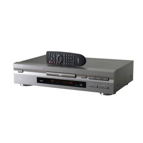
REAR PANELS U,C models (DVD-S795/S705) B, G models G model (Gold) A model 1 - 5... -
Page 8: Optical Pickup Self-Diagnosis And Replacement Procedure
OPTICAL PICKUP SELF-DIAGNOSIS AND REPLACEMENT PROCEDURE The optical pickup self-diagnosis function and tilt adjustment check function have been newly added to this player. When repair- ing, use the following procedure for effective Self-diagnosis and tilt adjustment. Be sure to use the self-diagnosis function before replacing the optical pickup when “NO DISC” is displayed. As a guideline, you should replace the optical pickup when the value of the laser drive current is more than 50. -
Page 9: Self-Diagnosis Function And Service Mode
SELF-DIAGNOSIS FUNCTION AND SERVICE MODES 1. Service Mode Table The service mode can be activated by pressing various button combinations on the player and remote control unit. Player buttons Remote control unit button Displaying the UHF display F_ _ _ Refer to Self-Diagnosis Function (UHF Display),in page 1-7. -
Page 10: Sales Demonstration Lock Function
3. Examples of Repairs Using Error Code Refer to this section when carrying out repairs. Malfunction example Error display F0** Disc, IC7001 F103 Disc, IC7001 F4FF IC6001 F500 Optical pickup, IC2001, IC5201, IC2511, IC2501 F501 IC2001, IC6201 F502 IC2501, IC2511, IC2001, IC5202 F504 IC5202, IC2001 F505... -
Page 11: Service Precautions
SERVICE PRECAUTIONS 1. Initializing the DVD Player Initialize the DVD player whenever you replace a microprocessor, microprocessor peripheral parts, module C.B.A or mother C.B.A. 1-1. Precautions The customer settings will return to factory preset settings when the player is initialized. Make a note of the settings and reset them after initializing. -
Page 12: Operating Instructions
OPERATING INSTRUCTIONS Connection •Ensure that this player and other equipment to be connected are set to the standby mode or off, and disconnect the AC cord, before commencing connection. •Do not block ventilation holes of any of the equipment and arrange them so that air can circulate freely. •Read through the instructions before connecting other equipment. - Page 13 OPERATING INSTRUCTIONS Connection Connecting to an AV amplifier which does not contain Dolby Digital or dts (digital theater systems) decoder This DVD/Video CD/CD player contains a Dolby Digital decoder. This enables the playback of DVDs recorded in Dolby Digital Sur- round or Linear PCM without the need for an optional decoder with Dolby Digital or Linear PCM processing.
-
Page 14: Common Procedures
OPERATING INSTRUCTIONS General information about On- D PLAY Screen Menu Icons POWER OPEN/CLOSE * / I This player features On-Screen Menu Icons providing various @ STOP g STILL/PAUSE D PLAY SELECT functions. A "banner" will be displayed on the TV monitor by pressing the ON SCREEN button on the remote control. - Page 15 OPERATING INSTRUCTIONS Detailed descriptions of each On-Screen Menu Icon Screen for disc information (For DVD) Title No. Change the title No. by using the cursor buttons ( , ) or the numeric buttons and press SELECT. Change the chapter No. by using the cursor buttons ( , ) or the numeric buttons and Chapter No.
- Page 16 OPERATING INSTRUCTIONS Detailed descriptions of each On-Screen Menu Icon Screen for disc information (For Video CD/CD) Change the track No. by using the cursor buttons Track No. ) or the numeric buttons and press SELECT. During CD play, display is changed by using the cursor Elapsed playing time buttons ( , (minute: second)
-
Page 17: Screen For Player Information
OPERATING INSTRUCTIONS Screen for player information Press SELECT during play to store location A and press SELECT again to store location B and to start A-B repeat play repeat play between the specified two locations. Press SELECT again to return to normal play. Select the preferred mode during play by Press SELECT during play using the cursor buttons ( ,... -
Page 18: Shuttle Screen
OPERATING INSTRUCTIONS Detailed descriptions of each On-Screen Menu Icon Shuttle screen Still/Pause Press the cursor button ( ). Slow-motion play Press the cursor button ( ). Slow-motion play Press the cursor button ( ). (Backward) (DVD only) (Forward) (DVD/Video CD only) µ... -
Page 19: Assembling And Disassembling The Casing And Checking C.b.a.s
SECTION2 ASSEMBLING AND DISASSEMBLING THE CASING AND CHECKING C.B.A.s 1. Disassembly Procedure When servicing the unit, use the following procedure to disassemble the casing and inside parts for internal inspection. Top cover Tray Front panel Rear panel Mechanism unit Power Supply V. -
Page 20: Casing Parts And C.b.a. Positions
2. Casing Parts and C.B.A. Positions 3. Service Positions Note To inspect the loading base unit, position the left side upward (as viewed from the front). Module C.B.A. TX946370 TX946370 Mother C.B.A. Power supply C.B.A. TX946360 2 - 2... -
Page 21: Disassembling The Top Cover
4. Disassembling the Top Cover 5. Disassembling the Tray 1. Remove the 4 screws. 1. Turn the level clockwise. 2. Move the tray in the direction of the arrow until it locks. Screw Top cover 3. Release the tab locks on the left and right, then pull out the tray. -
Page 22: Disassembling The Loading Base Unit
7. Disassembling the Loading 2. Connect the module C.B.A. to the mother C.B.A. with the extension cables for inspection. Base Unit •Extension cables: TX946370 (JGS0098) Mother C.B.A. Module C.B.A. 1. Remove the 4 screws. PP4201-PS4201 2. Pull out the loading base unit vertically. PP3201-PS3201 Note There is a danger of damaging the connectors. -
Page 23: Checking The Power Supply C.b.a
10. Checking the Power Supply 3. Checked by connecting the module C.B.A. and the mother C.B.A. with the extension cables. C.B.A. Extension cables: TBD (two) 1. Remove the 3 screws. Module C.B.A. Mother C.B.A. PS3201–PP3201 PS4201–PP4201 2. Carefully pull out the power supply C.B.A. Note Note There is a danger of damaging the connectors. -
Page 24: Assembling And Disassembling The Optical Pickup
ASSEMBLING AND DISASSEMBLING THE OPTICAL PICKUP (MECHANICAL PARTS) The optical pickup can be damaged by static electricity from your body. Be sure to take static electricity countermeasures when working around the optical pickup. 1. Handling the Optical Pickup The optical pickup can be damaged by static electricity from your body. Be sure to take static electricity countermeasures when working around the optical pickup. -
Page 25: Lubricating The Loading Base Unit
3. Lubricating the Loading Base Unit When replacing parts, Iubricate the parts maked “XXX” in the diagram Clamper weight Clamper yoke Magnet Clamp base unit Traverse unit Clamper Grease EM-30LG (TX946270) 0.01g Intermediate chassis Tray Grease EM-30LG (TX946270) Grease EM-30LG 0.01g (TX946270) 0.01g... -
Page 26: Static Electricity Countermeasures
4. Static Electricity Countermeasures The laser diode inside the traverse unit (optical pickup) can be damaged by static electricity from your body. Be sure to take static electricity countermeasures when working around the optical pickup. 4-1. Static Electricity Countermeasure Methods 1. -
Page 27: Disassembling The Clamp Base Unit
5. Disassembling the Clamp Base Unit 1. Remove the 2 screws. 2. Release the 3 tabs on the clamper. 3-clamper tabs Yoke Loading base Magnet Screw Screw Clamper weight Clamper yoke Magnet Clamper Screw Clamper base Clamp base unit 6. Disassembling the Clamper Weight, Clamper Yoke, Magnet 7. -
Page 28: Disassembling The Stepping Motor Unit
9. Disassembling the Optical 2. Disconnect the 2 flexible cables. Pickup Unit 1. Remove the hook of the FPC holder, then remove the FPC holder itself. 2. Remove the screw. 3. Release the tab, then remove spring holder 1. Note Be sure not to lose the spring. -
Page 29: Disassembling The Nut Unit
10. Disassembling the Nut Unit 12. Assembling the Optical Pickup 1. Remove the screw. 1. Install the optical pickup. Notes Note •The nut unit is not part of the optical pickup. Take care not of attach the tilt spring and guide shaft in Before replacing the optical pickup, remove the nut the wrong order. - Page 30 13. Disassembling the Spring 3. Insert the pickup FPC into connector FP5201 on the module C.B.A. Motor Unit 1. Remove the three screw. Note Be sure to adjust the optical pickup tilt after replacing the spindle motor unit. Spindle motor unit Traverse chassis 4.
-
Page 31: Optical Pickup Tilt Adjustment
14. Optical Pickup Tilt Adjustment Measurement point Adjustment point Mode Disc DVDT-S15 (AAX07320) Main unit Tangential adjustment screw T1 (inner periphery) play service display Tilt adjustment screw T2 (outer periphery) play DVDT-S01 (TX946080) Measuring equipment, tools Adjustment value Hex wrench (part number: TX946380) Adjust to the minimum jitter value. - Page 32 STEP6 STEP7 Screw lock Adjustment screws (0.02 g) Pull out the traverse unit. Remove in the order (Refer to disassembly procedure of top cover, tray Screw lock and clamper base. in this manual.) (0.02 g) STEP8 Lock the adjustment screw in position using screw lock (part number: TX946400).
-
Page 33: Disassembling The Intermediate Chassis
15. Disassembling the 17. Disassembling the Pulley Gear Intermediate Chassis and Deceleration Gear 1. Push the stopper downward, then rotate it until it contacts 1. Remove the screw. the vertical cam. 2. Remove the pulley gear. 2. Release the 2 tabs. 3. -
Page 34: Lubricating The Optical Pickup And Peripheral Parts
19. Lubricating the Optical Pickup and Peripheral Parts When replacing parts, lubricate the parts marked “xxx” in the diagram. Froil 946P (part number. TX946410) 0.01g Spindle motor unit MC grease PD No. 10 (part number. TX946400) (part number. TX946390) 0.04g MC grease PD No. -
Page 35: Electrical Adjustment
ELECTRICAL ADJUSTMENT 1. Video Output (Luminance Signal) Adjustment Do this adjustment after replacing a C.B.A. Measurement point Adjustment point Mode Disc Color bar 75% DVDT-S15 (AX07320) PLAY (Title 46): DVDT-S15 Video output terminal VR3501(mother C.B.A.) PLAY (Title 10): DVDT-S01 DVDT-S01 (TX946080) Adjustment value Measuring equipment, tools Screwdriver, Oscilloscope... -
Page 36: Video Component Signal (Cb) Output Adjustment
3. Video Component Signal (CB) Output Adjustment Do this adjustment after replacing a C.B.A. Measurement point Adjustment point Mode Disc Color bar 75% DVDT-S15 (AX07320) Video output terminal VR3201(mother C.B.A.) PLAY (Title 46): DVDT-S15 (Y) (CB) Output terminal PLAY (Title 10): DVDT-S01 DVDT-S01 (TX946080) Adjustment value Measuring equipment, tools... -
Page 37: Abbreviations
SECTION3 ABBREVIATIONS INITIAL/LOGO ABBREVIATIONS INITIAL/LOGO ABBREVIATIONS A0~UP ADDRESS ERROR TORQUE CONTROL ACLK AUDIO CLOCK ERROR TORQUE CONTROL AD0–UP ADDRESS BUS REFERENCE ADATA AUDIO PES PACKET DATA ENCSEL ENCODER SELECT ADDRESS LATCH ENABLE ETMCLK EXTERNAL M CLOCK (81MHz/40.5MHz) AMUTE AUDIO MUTE ETSCLK ETSCLK EXTERNAL S CLOCK (54MHz) AREQ... - Page 38 INITIAL/LOGO ABBREVIATIONS INITIAL/LOGO ABBREVIATIONS READ ENABLE VBLANK V BLANKING RFENV RF ENVELOPE COLLECTOR POWER SUPPLY RF PHASE DIFFERENCE OUTPUT VOLTAGE (CD-ROM) REGISTER SELECT VCDCONT VIDEO CD CONTROL (TRACKING RSEL PF POLARITY SELECT BALANCE) RESET DRAIN POWER SUPPLY VOLTAGE RESERVE VIDEO FEED BACK SBI0, 1 SERIAL DATA INPUT VREF...
-
Page 39: Block Diagram
BLOCK DIAGRAM 1. OVERALL BLOCK DIAGRAM 3 - 3 3 - 4... -
Page 40: Servoblock Diagram
2. SERVO BLOCK DIAGRAM 3 - 5 3 - 6... -
Page 41: Video Block Diagram
3. VIDEO BLOCK DIAGRAM 3 - 7 3 - 8... -
Page 42: Audio Block Diagram
4. AUDIO BLOCK DIAGRAM 3 - 9 3 - 10... -
Page 43: Schematic Diagram
SCHEMATIC DIAGRAM U, C MODELS 1. POWER SUPPLY SCHEMATIC DIAGRAM (FOR U, C MODELS) 12.5 17.0 —26.0 16.6 3 - 11 3 - 12... -
Page 44: Power Supply Schematic Diagram (For B, G, A)Models
B, G, A MODELS 2. POWER SUPPLY SCHEMATIC DIAGRAM (FOR B, G, A)MODELS 12.5 17.0 —26.0 16.6 3 - 13 3 - 14... -
Page 45: Adsc (Module C.b.a. 1/8) Schematic Diagram
3. ADSC (MODULE C.B.A. 1/8) SCHEMATIC DIAGRAM IC2001 STOP PLAY STOP PLAY STOP PLAY STOP PLAY STOP PLAY STOP PLAY STOP PLAY STOP PLAY STOP PLAY STOP PLAY STOP PLAY STOP PLAY STOP PLAY STOP PLAY STOP PLAY STOP PLAY STOP PLAY STOP... -
Page 46: Servo (Module C.b.a. 2/8) Schematic Diagram
4. SERVO (MODULE C.B.A. 2/8) SCHEMATIC DIAGRAM 8.9(8.8) 0.1(1.4) 1.4(1.2) 1.4(0.8) 1.4(1.5) 0.1(1.3) 0.1(1.3) 1.4(0.7) 1.4(1.2) 2.4(3.1) 2.4(3.1) 8.9(8.8) 0.1(1.5) 2.3(1.2) 0.1(2.5) 5.8(3.2) 0.1(0.5) 2.2(5.1) 5.8(3.2) 0.4(2.7) 3.1(0) 0(3.5) 0.2(3.1) (7.2) 2.2(2.9) 2.3(0) 5.0(2.9) 2.2(7.2) 5.0(0.3) 2.2(0) 5.0(2.9) 5.0(2.9) 2.2(7.2) 5.0(2.9) 8.9(8.8) 5.0(0.8) -
Page 47: Av Decoder (Module C.b.a. 3/8) Schematic Diagram
5. AV DECODER (MODULE C.B.A. 3/8) SCHEMATIC DIAGRAM IC3001 STOP PLAY STOP PLAY STOP PLAY 1.6(1.5) 5.0(4.9) STOP PLAY STOP PLAY STOP PLAY STOP PLAY STOP PLAY STOP PLAY STOP PLAY STOP PLAY STOP PLAY 3 - 19 3 - 20... -
Page 48: Vdac (Module C.b.a. 4/8) Schematic Diagram
6. VDAC (MODULE C.B.A. 4/8) SCHEMATIC DIAGRAM 2.4(2.7) 3.3(0.1) 2.8(3.3) 2.4(2.5) 1.1(1.3) 2.4(2.6) (1.8) (2.5) 1.5(2.1) 1.6 1,1 0(2.4) 0.5(0.6) (2,4) 2.4(2.3) 2.2(0) 0.1(0.3) (2.2) 4.8(4.7) 2.4(0) 1.8(0.1) 2.4(0.6) (2.6) 0.1(0.2) 0.1(0) 2.2(0) (4.9) (4.9) 2.1(0.3) 0(0.2) 0.8(0.7) 0(0.2) 0(0.2) 0(0.7) 0(0.2) 0(0.1) -
Page 49: Fep (Module C.b.a. 5/8) Schematic Diagram
7. FEP (MODULE C.B.A. 5/8) SCHEMATIC DIAGRAM 1.3(3.3) 4.5(3.3) 1.7(1.4) 0(0.1) 1.2(2.2) 0.3(0) 4.9(3.9) 0.3(0) IC5202 STOP PLAY STOP PLAY STOP PLAY STOP PLAY STOP PLAY 3 - 23 3 - 24... -
Page 50: Cpu (Module C.b.a. 6/8) Schematic Diagram
8. CPU (MODULE C.B.A. 6/8) SCHEMATIC DIAGRAM 0(1.1) 2.3(0) 2.7(2.5) 0(3.0) 2.8(1.8) 0(3.0) 1.8(1.1) 2.8(2.9) 2.0(1.7) 2.9(3.0) 0.1(1.8) 0(2.9) 1.9(1.5) 0(2.9) 0(2.9) 2.8(3.0) 2.8(2.9) 3.1(1.7) 0(0.3) 0(0.3) 2.8(0.3) 0(0.8) 2.8(2.9) 2.1(1.8) 2.7(2.9) 0(1.8) 2.7(2.9) 2.4(2.1) 2.7(2.9) 2.3(1.9) 2.7(2.9) 0.1(2.7) 2.7(0.3) 0.1(2.8) 2.3(1.8) IC6201... -
Page 51: Clock (Module C.b.a. 7/8) Schematic Diagram
9. CLOCK (MODULE C.B.A. 7/8) SCHEMATIC DIAGRAM 2.4(3.0) 1.5(1.1) 1.1(1.3) 2.4(1.4) 0(1.2) 0(1.2) 2.3(1.3) 0(1.2) 0(1.2) 1.5(1.2) 2.3(1.3) 0(1.4) (1.4) (1.4) 1.5(1.4) 1.4(1.3) 1.4(1.3) 1.5(1.6) 3 - 27 3 - 28... -
Page 52: Odc (Module C.b.a. 8/8) Schematic Diagram
10. ODC (MODULE C.B.A. 8/8) SCHEMATIC DIAGRAM 2.9(3.0) 2.9(3.0) IC7001 STOP PLAY STOP PLAY STOP PLAY STOP PLAY 2.9(3.0) STOP PLAY STOP PLAY STOP PLAY STOP PLAY 3 - 29 3 - 30... - Page 53 11. VIDEO OUT (MOTHER C.B.A. 1/5) SCHEMATIC DIAGRAM 1.7(1.9) 1.7(1.9) 1.7(1.9) 1.0(1.3) 1.1(1.3) 1.0(1.2) 1.6(1.8) 2.3(2.4) 2.0(2.4) 1.5(1.6) 2.0(2.4) 2.0(2.4) 3 - 31 3 - 32...
- Page 54 12. ADAC (MOTHER C.B.A. 2/5) SCHEMATIC DIAGRAM 0(1.1) 0.2(5.0) 0.2(5.0) 0(5.0) 0(5.0) 0(5.0) 1.6(1.5) 3 - 33 3 - 34...
- Page 55 13. AUDIO AC-3 (MOTHER C.B.A. 3/5) SCHEMATIC DIAGRAM —8.9 —8.9 —8.9 —8.9 —8.9 —8.9 —8.9 —8.4 —8.4 —0.2 —0.2 —0.2 —0.2 —0.9 —0.2 —0.2 —0.9 —0.2 —0.9 —8.9 —0.2 —0.2 —0.2 —0.2 —0.8 —0.2 3 - 35 3 - 36...
- Page 56 14. AUDIO OUT (MOTHER C.B.A. 4/5) SCHEMATIC DIAGRAM 0.7(—4.9) (3.0) (4.5) 5.1(0) 0(3.1) 2.3(5.1) 0.6(5.1) 0.7(—4.9) 2.1(0) 1.7(—4.9) —3.0(4.4) 0.7(—4.9) 0.7(—4.9) 0.7(—4.9) 0.7(—4.9) 0.7(—4.9) 0.7(—4.9) —8.9 11.0 —8.8 —9.5 —0.7 —9.5 —8.8 —8.9 —8.4 —10.6 —8.9 3 - 37 3 - 38...
- Page 57 15. OPERATION (MOTHER C.B.A. 5/5) SCHEMATIC DIAGRAM IC6001 STOP -31.4 -18.0 -28.8 -28.8 -28.8 PLAY -29.5 -10.1 24.6 -21.7 -27.0 STOP -16.2 -21.1 -21.4 -28.5 -28.4 -28.8 -28.8 -28.8 -28.8 -28.8 -28.8 -28.7 -21.4 PLAY -17.5 -14.5 -21.8 -14.5 -24.3 -26.6 -27.0 -27.0...
-
Page 58: Video Comp Schematic Diagram (For U, C Models)
U, C MODELS 16. VIDEO COMP SCHEMATIC DIAGRAM (FOR U, C MODELS) 3 - 41 3 - 42... -
Page 59: Scart Schematic Diagram (For B, G Models)
B, G MODELS 17. SCART SCHEMATIC DIAGRAM (FOR B, G MODELS) 11.7 0 0 0 11.1 11.1 11.1 11.7 (11.1) 0 0 0 –5 13.1 (13.4) 0 0 0 0 11.1 10.4 11.1 0 0 0 0 0 –5 5.1 0 2.1(2.5) 5.1 0 2.1(2.6) -
Page 60: Front Sw/Head Phone/Power Sw Schematic Diagram
18. FRONT SW/HEAD PHONE/POWER SW SCHEMATIC DIAGRAM —8.9 3 - 45 3 - 46... -
Page 61: Circuit Board Diagram
CIRCUIT BOARD DIAGRAM U, C MODELS 1. POWER SUPPLY C.B.A. (FOR U, C MODELS) To Mother C.B.A. 3-56(F-8) THE STRIPED FRAME INDICATES THE PRIMARY CIRCUIT TO DISTINGUISH CAUTION PS1101 THE PRIMARY FROM THE SECONDARY CIRCUIT. PAY ATTENTION NOT TO RECEIVE AN ELECTRIC SHOCK DURING REPAIR AND SERVICE OF THE PRODUCTS. -
Page 62: Power Supply C.b.a. (For B, G, A Models)
B, G, A MODELS 2. POWER SUPPLY C.B.A. (FOR B, G, A MODELS) To Mother C.B.A. 3-56(F-8) THE STRIPED FRAME INDICATES THE PRIMARY CIRCUIT TO DISTINGUISH CAUTION THE PRIMARY FROM THE SECONDARY CIRCUIT. PS1101 PAY ATTENTION NOT TO RECEIVE AN ELECTRIC SHOCK DURING REPAIR AND SERVICE OF THE PRODUCTS. -
Page 63: Module C.b.a
3. MODULE C.B.A. MODULE C.B.A. MODULE (1/2) C.B.A. To Mother C.B.A. 3-55(F-5) [COMPONENT SIDE] Transistors Q3201 Q3211 Q3221 Q3231 TC4006 TC4008 TC4012 TC4014 TC4016 TP6252 TP6251 Q3241 TC4007 TC4009 TC4013 TC4015 C3041 Q3301 TC3202 TC3206 TC3209 TC3204 Q3302 LB7001 TC3201 TC3207 TC3208 TC3205... - Page 64 MODULE C.B.A. MODULE(2/2) C.B.A. [FOIL SIDE] Transistors Q5201 A-17 Transistor-resistors QR2001 B-14 QR2501 C-12 QR2502 B-12 FP3202 FP7001 FP4202 QR2503 C-12 P6251 QR5201 B-15 QR6311 C6252 LB7004 Integrated Circuits IC2001 C-15 IC3051 E-15 C3003 PS6201 LB4016 NJ3201 IC3061 E-14 C6254 C3031 C6253 IC3201...
-
Page 65: Mother C.b.a
4. MOTHER C.B.A. MOTHER C.B.A. To Video Comp. C.B.A. 3-16(A-3) for U, C Models Transistors To Scart C.B.A. 3-59(A-4) for B, G Models Integrated Circuits Q3501 IC3531 Q3502 IC4201 JK4771 JK4502 JK4501 JK3541 IC4781 Q3503 IC4211 C3550 Q4915 W082 R4584 S4501 Q3511 PP3801... -
Page 66: Front Sw/Head Phone/Power Sw C.b.a
5. FRONT SW/HEAD PHONE/POWER SW C.B.A. FRONT SW C.B.A. To Mother C.B.A. 3-55(A-2) FRONT SW C.B.A. Connector FP6401 ADDRESS INFORMATION FP26401 S6402 S6416 S6406 R6402 R6401 OPEN/ OPEN/ PLAY PAUSE STOP CLOSE CLOSE R6403 S6403 S6401 R6403 R6405 R6404 SEARCH SEARCH SKIP SKIP... -
Page 67: Scart C.b.a. (For B, G Models)
B, G MODELS 6. SCART C.B.A. (FOR B, G MODELS) SCART C.B.A. Integrated Circuits Transistors Q3851 IC3801 Q3852 IC3811 Q3853 IC3812 IC3813 Q3861 Q3862 IC3821 IC3822 Q3863 Q3864 IC3831 IC3841 Transistor-resistors IC3871 QR3841 IC3881 QR3842 Connectors QR3843 J3871 QR3851 J3881 QR3852 PS3801 QR3853... -
Page 68: Video Comp C.b.a. (For U, C Models)
SECTION4 U, C MODELS 7. VIDEO COMP C.B.A. (FOR U, C MODELS) EXPLODED VIEWS & REPLACEMENT PARTS LIST 1. Electrical Replacement Parts List WARNING Components having special characteristics are martked and must be replaced with parts having specifications equal to those originally installed. - Page 69 Schm Schm REMARKS REMARKS PART NO. D e s c r i p t i o n PART NO. D e s c r i p t i o n Ref. Ref. AAX01190 P.C.B. POWER SWITCH VEP96552A C1141 AAX05300 C.EL 150uF 35V VCEA1VJH151 AAX01210...
- Page 70 Schm Schm REMARKS REMARKS PART NO. D e s c r i p t i o n PART NO. D e s c r i p t i o n Ref. Ref. C2508 FX612210 C.CE 0.1uF 16V CH ECUX1C104KBV C3054 FX612220 C.CE 0.1uF 16V CH...
- Page 71 Schm Schm REMARKS REMARKS PART NO. D e s c r i p t i o n PART NO. D e s c r i p t i o n Ref. Ref. C3511 FX612070 C.CE 0.01uF 50V CH ECUM1H103KBN C3815 FX612090 C.CE 0.1uF 50V CH(BG) ECUM1H104ZFN...
- Page 72 Schm Schm REMARKS REMARKS PART NO. D e s c r i p t i o n PART NO. D e s c r i p t i o n Ref. Ref. C4219 NX704170 C.POL 0.022uF 50V ECHR1H223JZ C4397 FX611530 C.EL 100uF 16V ECA1CAK101X...
- Page 73 Schm Schm REMARKS REMARKS PART NO. D e s c r i p t i o n PART NO. D e s c r i p t i o n Ref. Ref. C4771 FX612090 C.CE 0.1uF 50V CH ECUM1H104ZFN C5237 FX612300 C.CE 1000pF 50V CH...
- Page 74 Schm Schm REMARKS REMARKS PART NO. D e s c r i p t i o n PART NO. D e s c r i p t i o n Ref. Ref. C6563 FX612220 C.CE 0.1uF 16V CH ECUX1C104ZFV D1131 NX702610 DIODE 11EQS10(ABG)
- Page 75 Schm Schm REMARKS REMARKS PART NO. D e s c r i p t i o n PART NO. D e s c r i p t i o n Ref. Ref. FP4701 AAX05440 VJS3537A009G IC4901 AAX03550 PQ09DZ1U PQ09DZ1U FP4721 AAX05460 VJS3537B009G IC5201...
- Page 76 Schm Schm REMARKS REMARKS PART NO. D e s c r i p t i o n PART NO. D e s c r i p t i o n Ref. Ref. K4384 AAX03820 R.CHP 0Ω 1/10W ERJ6GMZ0R00 L6007 AAX05380 COIL 47uH VLQEL05S470J...
- Page 77 Schm Schm REMARKS REMARKS PART NO. D e s c r i p t i o n PART NO. D e s c r i p t i o n Ref. Ref. LB4004 GX609450 COIL VLP0155 LB6525 GX609460 COIL VLP0157 LB4005 GX609450 COIL...
- Page 78 Schm Schm REMARKS REMARKS PART NO. D e s c r i p t i o n PART NO. D e s c r i p t i o n Ref. Ref. Q3513 iX637230 2SB709AR 2SB709AR QR3853 AAX05760 TR.DGT XN1112(BG) XN1112 Q3551 AAX04280...
- Page 79 Schm Schm REMARKS REMARKS PART NO. D e s c r i p t i o n PART NO. D e s c r i p t i o n Ref. Ref. R2014 AAX06450 R.MTL.CHP 4.7KΩ 1/16W ERJ3GEYJ472 R3009 HX610100 R.MTL.CHP 220Ω...
- Page 80 Schm Schm REMARKS REMARKS PART NO. D e s c r i p t i o n PART NO. D e s c r i p t i o n Ref. Ref. R3317 AAX06470 R.MTL.CHP 68Ω 1/16W ERJ3GEYJ680 R3572 AAX06990 R.MTL.CHP 18KΩ...
- Page 81 Schm Schm REMARKS REMARKS PART NO. D e s c r i p t i o n PART NO. D e s c r i p t i o n Ref. Ref. R3866 AAX06850 R.MTL.CHP 4.7KΩ 1/10W(BG) ERJ6GEYJ472 R4342 AAX06970 R.MTL.CHP 100KΩ...
- Page 82 Schm Schm REMARKS REMARKS PART NO. D e s c r i p t i o n PART NO. D e s c r i p t i o n Ref. Ref. R4501 AAX07170 R.MTL.CHP 820Ω 1/10W ERJ6GMYJ821 R4903 AAX07070 R.MTL.CHP 33KΩ...
- Page 83 Schm Schm Schm Schm REMARKS REMARKS REMARKS REMARKS PART NO. D e s c r i p t i o n PART NO. D e s c r i p t i o n PART NO. D e s c r i p t i o n PART NO.
-
Page 84: Casing Parts & Mechanism Section
KNOB, VOLUME VGU8147 * 18 AAX06060 KNOB, VOLUME VGU8149 HEADPHONE C.B.A. TO POWER SW * 19 AAX04720 BUTTON, OPERATION L DVD-S795 GD VGU8090 C.B.A. * 19 AAX06230 BUTTON, OPERATION L DVD-S795 BL VGU8141 TO MOTHER HEADPHONE * 19 AAX06240 BUTTON, OPERATION... - Page 85 Ref. PART NO. D e s c r i p t i o n Remarks Markets * 26 AAX05110 GROUND WIRE VEE0G61 (UC) * B 1 EX603920 SCREW VHD0690 * B 2 EX603940 SCREW VHD1041 * B 2 EX603960 SCREW VHD1094 * B 3 AAX04390 SCREW...
-
Page 86: Loading Mechanism Section
Loading Mechanism Section 3-1. Loading Mechanism Section Exploded View MODULE C.B.A. LOADING MOTOR C.B.A. 4 - 21... -
Page 87: Loading Mechanism Section
3-2. Loading Mechanism Section Parts List Ref. PART NO. D e s c r i p t i o n Remarks Markets * 41 AAX04750 MIDDLE CHASSIS VMD3270 * 42 AAX04300 TRAY VMD3265 * 43 AAX04530 PULLEY GEAR VDG1308 * 44 AAX04640 REDUCTION GEAR VDG1309... -
Page 88: Traverse Section
Traverse Section 4-1. Traverse Section Exploded View SPINDLE STEPPING MOTOR MOTOR MODULE C.B.A. 4 - 23... -
Page 89: Traverse Section
4-2. Traverse Section Parts List Ref. PART NO. D e s c r i p t i o n Remarks Markets * 61 AAX04130 FFC, SPINDLE VWJ1277 * 62 AAX04140 MOTOR, SPIDLE VEM0665 * 63 AAX04120 MOTOR, STEPPING VEM0666 * 64 AAX03740 SPRING VMB3278... -
Page 90: Remote Control Transmitter
±æ◊ ¡œ”…OKXIA ”Ã˝∆§¥¯◊ ‘¥ø‚www.okxia.cnÃ·π © Remote Control Transmitter TP10 TP18 TP17 TP16 KI/O6 KI/O5 TP15 KI/O7 KI/O4 TP14 KI/O3 TP13 MSD602 KI/O2 R2 300 TP12 KI/O1 TP11 KI/O0 X–OUT 3.52MHz X–IN UR64LD1 RESET – R1 1.0 100µF KASEIKYOU FORMAT (A.E.H.A) 36.7kHz/ 1/2DUTY CUSTOM DATA FUNCTION...