Advertisement
Quick Links
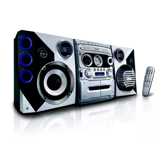
Mini System
Service
Service
Service
Service
Service
Service Manual
©
Copyright 2004 Philips Consumer Electronics B.V. Eindhoven, The Netherlands
All rights reserved. No part of this publication may be reproduced, stored in a retrieval system or
transmitted, in any form or by any means, electronic, mechanical, photocopying, or otherwise
without the prior permission of Philips.
Published by SL-ET0447 Service Audio Printed in The Netherlands Subject to modification.
Version 1.0
TABLE OF CONTENTS
Location of PC Boards ................................................ 1-2
Versions Variation & Package .................................... 1-2
Specifications .............................................................. 1-3
Measurement Setup ................................................... 1-4
Service Aids ................................................................ 1-5
ESD & Safety Instruction ............................................ 1-6
Setting Procedure & Repair Instructions ....................... 2
Disassembly Instructions & Service positions .............. 3
Block & Wiring Diagram ................................................ 4
Key/Video/Sensor/Phone/Vol /Vu Board ....................... 5
Tuner Board ................................................................... 6
Main Board .................................................................... 7
Power Board .................................................................. 8
Mechanical Exploded View & Parts List ...................... 11
FWD570/
Page
VIDEO CD
CLASS 1
LASER PRODUCT
GB
21M
3141 785 30100
Advertisement

Related Manuals for Philips FWD570/21M


Summary of Contents for Philips FWD570/21M
- Page 1 LASER PRODUCT © Copyright 2004 Philips Consumer Electronics B.V. Eindhoven, The Netherlands All rights reserved. No part of this publication may be reproduced, stored in a retrieval system or transmitted, in any form or by any means, electronic, mechanical, photocopying, or otherwise without the prior permission of Philips.
- Page 2 LOCATION OF PRINTED CIRCUIT BOARDS MOTOR2 BOARD MOTOR1 BOARD KARAOKE BOARD GAME PORT BOARD POWER BOARD HEADPHONE BOARD VERSION VARIATIONS: Type /Versions: FWD570 /21M Features & Board in used: Aux in /CDR in Line Out DIN Out Subwoofer Out Video Out S-Video Out Component Video Out Digital Out...
-
Page 3: Specifications
............4 Hz - 44 kHz (96kHz) Output power ..........3300 W PMPO Digital Output ..............Stereo mode (DIN) ......100 W + 100 W RMS ....SPDIF (Sony Philips digital interface) Coaxial Surround mode (1 kHz) ........DIN OUT PCM ..............IEC 60958 ±... -
Page 4: Measurement Setup
MEASUREMENT SETUP Tuner FM Bandpass LF Voltmeter 250Hz-15kHz e.g. PM2534 e.g. 7122 707 48001 RF Generator e.g. PM5326 S/N and distortion meter e.g. Sound Technology ST1700B Use a bandpass filter to eliminate hum (50Hz, 100Hz) and disturbance from the pilottone (19kHz, 38kHz). Tuner AM (MW,LW) Bandpass LF Voltmeter... -
Page 5: Service Aids
SERVICE AIDS ESD Equipment: Service Tools: Universal Torx driver holder .........4822 395 91019 Anti-static table mat - large 1200x650x1.25mm ...4822 466 10953 anti-static table mat - small 600x650x1.25mm ..4822 466 10958 Torx bit T10 150mm ...........4822 395 50456 Anti-static wristband ..........4822 395 10223 Torx driver set T6-T20 .........4822 395 50145 Connectorbox (1M Ω) -
Page 6: Laser Product
WAARSCHUWING WARNING Alle IC’s en vele andere halfgeleiders zijn All ICs and many other semi-conductors are gevoelig voor electrostatische ontladingen susceptible to electrostatic discharges (ESD). (ESD). Careless handling during repair can reduce life Onzorgvuldig behandelen tijdens reparatie kan drastically. de levensduur drastisch doen verminderen. When repairing, make sure that you are Zorg ervoor dat u tijdens reparatie via een connected with the same potential as the mass... - Page 7 PREPARATIONS AND CONTROLS...
- Page 8 PREPARATIONS AND CONTROLS...
- Page 9 PREPARATIONS AND CONTROLS...
- Page 10 1-10 PREPARATIONS AND CONTROLS...
- Page 11 1-11 F UNCTIONAL OVERVIEW...
- Page 12 1-12 F UNCTIONAL OVERVIEW...
- Page 13 1-13 TROUBLESHOOTING...
- Page 14 System, Region code, Tuner, etc. setting procedure 5. Video Out Change 3) Region code change timer reset a) Press "SYSTEM" on R/C button Press below key to reset the timer : Hence in total, reprograming will be done by way of the 1) System Reset b) Select the menu using the "...
- Page 15 REPAIR INSTRUCTIONS...
- Page 16 REPAIR INSTRUCTIONS...
- Page 17 DISMANTLING INSTRUCTIONS Dismantling of the Cassette Cover Pull out Press and hold it between the tape deck and the cassette door Figure 2 Figure 4 Figure 1 Dismantling the 3CDC Module Dismantling of the Cover Front Display and Cover Front Ornamental (pos 130) 4) Remove the Cover Tray as shown in figure 4.
- Page 18 Detaching the Main board and Front Cabinet Assembly from the Bottom/Rear assembly Dismantling of the Rear Panel 1) Release 2 catches 'B' to free the Main board from the Front 1) Loosen 8 screws 'J' to remove the Rear Panel figure 11. Cabinet Assembly as shown in figure 6.
-
Page 19: Service Positions
Service positions Service position A Service position B Note: After re-assembly, it is very important to ensure the wires are properly inserted into their respective sockets and routed not to touch or obstruct any moving parts. Service position C... - Page 20 SET BLOCK DIAGRAM...
- Page 21 SET WIRING DIAGRAM...
- Page 22 FTD DISPLAY PIN ASSIGNMENT KEY / VIDEO / SENSOR / PHONE / VOL / VU BOARD TABLE OF CONTENTS FTD Display Pin Assignment ........... 5-1 FTD Display Pin Connection ........... 5-1 Internal IC Diagram & Pin Description ......5-2 Circuit Diagram ..............5-3 PCB Layout Top View ............
- Page 23 PIN DESCRIPTION INTERNAL BLOCK DIAGRAM VFD CONTROLLER - IC TP6311QH VFD CONTROLLER - IC TP6311QH SG1/KS1 Control SG2/KS2 SG3/KS3 T s i i p SG4/KS4 t f i i t r ) t i Serial Genaral Segment SG5/KS5 Data Input SG6/KS6 Driver/ interface...
- Page 24 CIRCUIT DIAGRAM - KEY BOARD C1805 R284 SW803 C2001 R285 SW804 C2002 R286 TA251 C2003 R287 TA253 C2004 R288 TA255 C2005 R289 TA258 C2006 R291 TA259 C2007 R292 TA260 C2008 R293 TA261 C2009 R294 TA262 C2010 R295 TA263 C2012 R296 TA265 C2013 R297...
- Page 25 PCB LAYOUT - KEY BOARD (TOP) C2017 C2018 IC254 LD256 R2042 R2043 R2044 R2045 R2046 RB252 RB253 RB254 RB257 RB803 RB804 SW803 SW804 TA255 TA258 TA259 TA260 TA261 TA262 TA263 TA265 TA266 TA267 TA268 TA269 TA270 TA271 TA272 TA273 TA274 TA276 TA277 TA278...
- Page 26 C1805 R2025 PCB LAYOUT - GAME & MIC & PHONE BOARD (TOP VIEW) C2003 R2026 C2004 R2027 C2009 R2029 C2010 R2030 C2016 R2040 C2023 R2041 C2028 R2056 C2032 R2057 C2034 R2062 C2035 R2063 CN202 R2064 CN252 R2066 CN253 R2067 CN254 R2068 CN257 R2071...
- Page 27 PCB LAYOUT - GAME & MIC & PHONE BOARD (BOTTOM VIEW) C2001 C2002 C2005 C2006 C2007 C2008 C2011 C2012 C2013 C2014 C2015 C2019 C2020 C2021 C2024 C2025 C2026 C2027 C2029 C2030 C2031 C2225 C2226 C2227 C2228 ESDC2 D1 ESDC5 D1 IC251 IC255 Q251...
- Page 28 ELECTRIC PARTS - KEY BOARD SW803 9940 000 00871 TACT SW DIA1.7MM SW804 9940 000 00871 TACT SW DIA1.7MM TA280 9940 000 00872 TACT SW 50MA 12V TA281 9940 000 00872 TACT SW 50MA 12V TA282 9940 000 00872 TACT SW 50MA 12V TA283 9940 000 00872 TACT SW 50MA 12V...
- Page 29 TUNER ADJUSTMENT TABLE Waverange Input frequency Input Tuned to Adjust Output Scope/Voltmeter VARICAP ALIGNMENT ± 108MHz 7.5V check 87.5 - 108MHz ± (50kHz grid) 87.5MHz check 1.4V 0.2V ± 1602KHz 7.2V check ± 1.1V 0.2V 531KHz T005 531-1602kHz TUNER BOARD (9940 000 00873) (10kHz grid) ( 21L / 21L / 37S ) FM - RF...
- Page 30 TUNER ADJUSTMENT TABLE ANT001 R001 R002 R003 R004 C002 R005 C004 R006 C005 R007 C006 R008 C007 R009 C008 R010 C009 R011 C010 R012 C011 R013 C012 R014 C013 R015 C014 R016 C015 R017 C016 R018 C017 R019 C018 R020 C019 R021 C020...
- Page 31 CIRCUIT DIAGRAM - TUNER BOARD (TOP VIEW) ANT001 A2 C010 C029 C043 D001 Q003 T004 C014 C030 C044 D002 T005 C017 C033 C045 D004 R005 T006 C019 C036 C046 IC001 R024 VC001 C004 C024 C037 C047 IF001 R035 VD001 C005 C025 C038 C048...
- Page 32 PCB LAYOUT - TUNER BOARD (BOTTOM VIEW) C016 C032 D005 R002 R011 R019 R029 R040 VR001 C002 C018 C034 IC001 R003 R012 R020 R030 R046 C006 C020 C035 IC002 R004 R013 R021 R033 T002 C007 C021 C040 Q001 R006 R014 R023 R034 T003...
- Page 33 ES6698 INTERNAL IC DIAGRAM DVD/CD Motor Motor Driver Video ES6603S T V Display RF Amp MAIN BOARD 8/16-MB Audio DAC Speakers DRAM ES6698 Audio ADC Microphone In Vibratto-II EEPROM S/PDIF A/V Receiver ROM/Flash VFD Panel VFD Driver IR Remote TABLE OF CONTENTS TDA8920 INTERNAL IC DIAGRAM IC Internal Diagram ............
- Page 34 CIRCUIT DIAGRAM - MAIN BOARD...
- Page 35 SCHEMATIC MAPPING - MAIN PART SCHEMATIC MAPPING - SERVO PART C276 D1 C2221 E7 IC209 D4 R281 RA209 E7 C20 D1 C312 B1 C329 B1 CN8101 D1 D318 D3202 B3 IC503-C D4 R331 R436 R551 C277 C2222 E7 IC210 D4 R283 XL201 E5 D319...
- Page 36 CIRCUIT DIAGRAM - MAIN BOARD (SERVO PART)
- Page 37 CIRCUIT DIAGRAM - MAIN BOARD (TAPE PART)
- Page 38 SCHEMATIC MAPPING - TAPE PART LAYOUT MAPPING - TOP VIEW C438 C762 CN301 IC305 R245 R820 C701 D701 R726 R1092 C439 C801 CN501 IC401 R252 R821 C702 D702 R727 R1093 C440 C804 CN551 IC402 R253 R822 C703 D703 R728 R7001 C211 C441 C805...
- Page 39 PCB LAYOUT - MAIN BOARD (TOP VIEW)
- Page 40 PCB LAYOUT - MAIN BOARD (BOTTOM VIEW)
- Page 41 LAYOUT MAPPING - BOTTOM VIEW C282 C3 C485 C2203 B1 D709 R372 R468 R748 R3204 C283 C2 C488 C2204 B1 D710 R373 R469 R749 R3205 C285 C2 C489 C2205 B2 D712 R374 R471 C4 R752 R3206 C288 C3 C491 C2206 B2 D713 R375 R472 D4...
- Page 42 7-10 7-10 ELECTRIC PARTS - MAIN BOARD CF501 9940 000 00822 RESONATOR 2PIN 600KHZ IC803 9940 000 00855 IC 8PIN BA6287FE2 CF502 9940 000 00823 RESONATOR 2PIN 700KHZ IC804 9940 000 00855 IC 8PIN BA6287FE2 CN253 9940 000 00824 FFC CABLE 9P P1.27MM 80MM IC805 9940 000 00856 IC 8PIN LM358MX NS CN254...
- Page 43 IC INTERNAL BLOCK DIAGRAM SMPS CONTROLLER - KA7500C OUTPUT CONTROL OSCILLATOR DEAD TIME 1.2V CONTROL POWER BOARD V CC COMP EA(+) BAND GAP V REF EA(-) REFERENCE 0.7MA EA(+) EA(-) COMP INPUT IC INTERNAL BLOCK DIAGRAM FAIRCHILD POWER SWITCH - KA5M02659RN TABLE OF CONTENTS IC Internal Block Diagram ...........
- Page 44 CIRCUIT DIAGRAM - POWER BOARD BD901 A1 C908 A2 C919 D1 C953 A4 C963 B5 C978 D4 C988 A3 C998 CN903 A1 D908 D960 IC954 B4 L959 Q954 R903 R914 R951 R961 R973 R983 R993 TR902 BF901 A2 C909 A2 C920 C1 C954 A4 C964 C5...
- Page 45 PCB LAYOUT - POWER BOARD BD901 C913 C953 C974 C991 CN902 B1 D953 J801 JMP12 C2 JMP30 A1 Q905 R906 R922 R965 R982 R999 C851 C914 C954 C975 C992 CN903 A1 D954 J802 JMP13 D5 JMP31 A1 Q951 R906A R923 R966 R983 RT901...
- Page 46 ELECTRIC PARTS - POWER BOARD BD901 9940 000 00931 BRIDGE KBU808 8A 1000V R972 9940 000 00956 FUSE RES 5.6 1/4W 5% C902 9940 000 00932 COND SAFTY 0.47UF 275V 10% RT901 9940 000 00957 NTC 5R 5A C903 9940 000 00932 COND SAFTY 0.47UF 275V 10% TR901 9940 000 00958...
- Page 47 MECHANICAL EXPLODED VIEW SCREW LIST Description SCREW M3.0xP0.5x22mm SCREW T2.0x0.63PxL7mm SCREW L8xP1.06xT3.0mm D=7.5mm SCREW T3.0xL8xP1.06mm,0.47g SCREW M3.0xP0.5x8 SCREW T3.0xL8xP1.06mm SCREW M3.0xP0.5x6,0.5g SCREW T3.0xL8.0xW/@10.0mm SCREW T3.0xL10xP1.06mm SCREW M3x6x0.5P SCREW M3.0xP0.5x10 SCREW T3.0xL10xP1.06mm...
- Page 48 9940 000 00912 PANEL LEFT 9940 000 00874 3 CDC MODULE 9940 000 00873 TUNER MODULE 9940 000 00917 FAN 60X60X15MM DC 12V 9940 000 00927 TAPE DECK PHILIPS 9940 000 00877 RUBBER DIA14XT2MM BLACK 9940 000 00899 COVER TOP...