Table of Contents
Advertisement
SERVICE MANUAL
Ver 1.1 2002.05
Sony Corporation
9-929-212-12
2002E0500-1
Home Audio Company
C 2002.05
Published by Sony Engineering Corporation
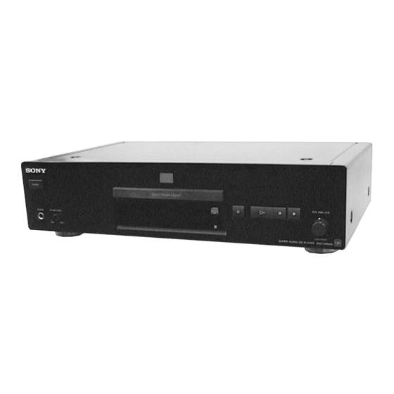
SCD-XB940
Photo: Black type
Model Name Using Similar Mechanism
CD Mechanism Type
Base Unit Name
Optical Pick-up Name
SPECIFICATIONS
AEP Model
NEW
CDM55B-DVBU3
DVBU3
KHM-220AAA/J1N
– Continued on next page –
SUPER AUDIO CD PLAYER
UK Model
Advertisement
Chapters
Table of Contents

Related Manuals for Sony SCD-XB940


Summary of Contents for Sony SCD-XB940
- Page 1 Model Name Using Similar Mechanism CD Mechanism Type CDM55B-DVBU3 Base Unit Name DVBU3 Optical Pick-up Name KHM-220AAA/J1N SPECIFICATIONS – Continued on next page – SUPER AUDIO CD PLAYER Sony Corporation 9-929-212-12 2002E0500-1 Home Audio Company C 2002.05 Published by Sony Engineering Corporation...
- Page 2 AND IN THE PARTS LIST ARE CRITICAL TO SAFE OPERATION. REPLACE THESE COMPONENTS WITH Flexible Circuit Board Repairing SONY PARTS WHOSE PART NUMBERS APPEAR AS SHOWN IN THIS MANUAL OR IN SUPPLEMENTS PUB- • Keep the temperature of the soldering iron around 270 ˚C dur- LISHED BY SONY.
-
Page 3: Table Of Contents
TABLE OF CONTENTS SERVICING NOTES ..........4 GENERAL ..............5 DISASSEMBLY ............8 DIAGRAMS 4-1. Notes for Printed Wiring Board and Schematic Diagram ............11 4-2. Printed Wiring Board – TK Board – ......12 4-3. Schematic Diagram – TK Board – ........ 13 4-4. -
Page 4: Servicing Notes
Ver 1.1 SECTION 1 SERVICING NOTES HOW TO OPEN THE TRAY WHEN POWER SWITCH NOTES ON HANDLING THE OPTICAL PICK-UP TURNS OFF BLOCK OR BASE UNIT There are two different methods to open the tray. The laser diode in the optical pick-up block may suffer electro- static break-down because of the potential difference generated •... -
Page 5: General
SECTION 2 This section is extracted from instruction manual. GENERAL... -
Page 8: Disassembly
SECTION 3 DISASSEMBLY Note: Follow the disassembly procedure in the numerical order given. COVER (4095269) 1 two screws 1 two screws 1 two screws 3 cover (4095269) 1 two screws FRONT PANEL SECTION 4 connector 5 holder (CN992) 7 two claws 1 Pull out the tray. -
Page 9: Main Board (Component Side)
AUDIO/MAIN BOARD 6 three connectors (CN301, 304, 351) 8 screw 2 two wires (flat type) (18 core) (BVTT3 (CN602, 603) 3 two connectors (CN605, 610) q; AUDIO board 4 five screws 2 two wires (flat type) (16 core) (BVTT3 (CN608, 611) 5 MAIN board 2 wire (flat type) (10 core) (CN601) - Page 10 TRAY claw claw 1 Remove the tray. (Careful of the claw.)
-
Page 11: Notes For Printed Wiring Board And Schematic Diagram
SECTION 4 DIAGRAMS 4-1. NOTE FOR PRINTED WIRING BOARDS AND SCHEMATIC DIAGRAMS • Circuit Boards Location Note on Printed Wiring Board: Note on Schematic Diagram: TRANSFORMER board POWER board • X : parts extracted from the component side. • All capacitors are in µF unless otherwise noted. pF: µµF •... -
Page 12: Printed Wiring Board – Tk Board
SCD-XB940 4-2. PRINTED WIRING BOARD – TK Board – • See page 11 for Circuit Boards Location. (Page 14) (Page 14) -
Page 13: Schematic Diagram – Tk Board
SCD-XB940 4-3. SCHEMATIC DIAGRAM – TK Board – • See page 32 for Waveforms. (Page 16) (Page 16) The components identified by mark 0 or dotted line with mark 0 are critical for safety. Replace only with part number specified. -
Page 14: Printed Wiring Board Main Board (Component Side)
SCD-XB940 4-4. PRINTED WIRING BOARD – MAIN Board (Component Side) – • See page 11 for Circuit Boards Location. (Page 28) (Page 22) (Page 22) • Semiconductor Location Ref. No. Location IC605 IC607 IC612 IC617 IC621 IC622 IC632 (Page 12) -
Page 15: Printed Wiring Board Main Board (Conductor Side)
SCD-XB940 4-5. PRINTED WIRING BOARD – MAIN Board (Conductor Side) – • See page 11 for Circuit Boards Location. • Semiconductor Location Ref. No. Location D600 D604 D605 D606 D607 D608 D609 D610 D612 IC600 IC606 IC609 IC610 IC613 IC614... -
Page 16: Schematic Diagram – Main Board (1/6)
SCD-XB940 4-6. SCHEMATIC DIAGRAM – MAIN Board (1/6) – • See page 32 for Waveforms. (Page 18) (Page 29) (Page 13) (Page 17) (Page 13) (Page 27) (Page 20) (Page (Page 21) (Page 19) (Page 20) -
Page 17: Schematic Diagram - Main Board (1/6)
SCD-XB940 4-7. SCHEMATIC DIAGRAM – MAIN Board (2/6) – (Page 16) (Page 21) (Page 18) (Page 21) (Page 20) -
Page 18: Schematic Diagram – Main Board (3/6)
SCD-XB940 4-8. SCHEMATIC DIAGRAM – MAIN Board (3/6) – • • See page 32 for Waveforms. See page 34 for IC Block Diagram. (Page 23) (Page 16) (Page 23) (Page 25) (Page 17) (Page 19) (Page 20) (Page 21) -
Page 19: Schematic Diagram – Main Board (4/6)
SCD-XB940 4-9. SCHEMATIC DIAGRAM – MAIN Board (4/6) – • See page 32 for Waveform. (Page 16) (Page 18) (Page 20) -
Page 20: Schematic Diagram - Main Board (3/6)
SCD-XB940 4-10. SCHEMATIC DIAGRAM – MAIN Board (5/6) – (Page 16) (Page 17) (Page 16) (Page 16) (Page 18) (Page 19) (Page 21) -
Page 21: Schematic Diagram - Main Board (4/6)
SCD-XB940 4-11. SCHEMATIC DIAGRAM – MAIN Board (6/6) – • • See page 32 for Waveforms. See page 34 for IC Block Diagram. (Page 18) (Page 17) (Page 16) (Page 17) (Page 20) -
Page 22: Printed Wiring Board – Audio Board
SCD-XB940 4-12. PRINTED WIRING BOARD – AUDIO Board – • See page 11 for Circuit Boards Location. (Page 14) (Page 14) (Page 24) • Semiconductor Location (Page 28) Ref. No. Location D302 (Page D303 D321 E-13 IC301 E-17 IC302 E-11... -
Page 23: Schematic Diagram - Audio Board
SCD-XB940 4-13. SCHEMATIC DIAGRAM – AUDIO Board – • • See page 32 for Waveforms. See page 34 for IC Block Diagrams. (Page 29) (Page 18) (Page 29) (Page 18) (Page 24) The components identified by mark 0 or dotted line with mark 0 are critical for safety. -
Page 24: Printed Wiring Board - Hp Board
SCD-XB940 4-14. PRINTED WIRING BOARD – HP Board – • See page 11 for Circuit Boards Location. 4-15. SCHEMATIC DIAGRAM – HP Board – (Page 23) (Page 22) -
Page 25: Printed Wiring Board - Loading Board
SCD-XB940 4-16. PRINTED WIRING BOARD – LOADING Board – • See page 11 for Circuit Boards Location. 4-17. SCHEMATIC DIAGRAM – LOADING Board – (Page 14) (OPEN/CLOSE) (Page 18) -
Page 26: Printed Wiring Board - Display Board
SCD-XB940 4-18. PRINTED WIRING BOARD – DISPLAY Board – • See page 11 for Circuit Boards Location. (Page 28) (Page 14) • Semiconductor Location Ref. No. Location D201 IC201 IC202 IC203 IC271 Q201 Q202 Q203... -
Page 27: Schematic Diagram - Display Board
SCD-XB940 4-19. SCHEMATIC DIAGRAM – DISPLAY Board – • See page 32 for Waveforms. (Page 29) (Page 16) -
Page 28: Printed Wiring Board - Power Board
SCD-XB940 4-20. PRINTED WIRING BOARD – POWER Board – • See page 11 for Circuit Boards Location. (Page 26) (Page 14) (Page 22) • Semiconductor Location Ref. No. Location D901 D902 D903 D904 D905 D906 D907 D908 D909 D910 D911... -
Page 29: Schematic Diagram - Power Board
SCD-XB940 4-21. SCHEMATIC DIAGRAM – POWER Board – (Page 27) (Page 31) (Page 16) (Page 23) (Page 31) (Page 23) The components identified by mark 0 or dotted line with mark 0 are critical for safety. Replace only with part number specified. -
Page 30: Printed Wiring Boards
SCD-XB940 4-22. PRINTED WIRING BOARDS – AC SW/TRANSFORMER Boards – • See page 11 for Circuit Boards Location. (Page 28) (Page 28) AC SW BOARD TRANSFORMER BOARD... -
Page 31: Schematic Diagram - Ac Sw/Transformer Boards
SCD-XB940 4-23. SCHEMATIC DIAGRAM – AC SW/TRANSFORMER Boards – (Page 29) (Page 29) The components identified by mark 0 or dotted line with mark 0 are critical for safety. Replace only with part number specified. - Page 32 • Waveforms – MAIN Board – – AUDIO Board – – TK Board – qa IC617 qf (MCKI) 1 IC001 el (TE) (CD PLAY) 1 IC607 <z/, (X2/CLKIN) 6 IC617 rs (BCKD) IC622 <zxc (SCKI), IC623 8 1 IC301 qs (XOUT) 6 IC309 5 (Q) 2.9 Vp-p Approx.
- Page 33 – DISPLAY Board – 1 IC201 tk (OSCO) 4.1 Vp-p 484 ns 2 IC203 ea (EXTAL) 3.8 Vp-p 8 MHz...
- Page 34 • IC Block Diagrams – MAIN Board – IC621 SN74LV74APWR 13 12 11 1 2 3 4 5 6 IC628 MSM54V16258BSL-40TS-K 34 – 32 30 29 REFRESH INTERNAL TIMING CONTROL ADDRESS GENERATOR CLOCK COUNTER CONTROLLER OUTPUT INPUT BUFFER BUFFER COLUMN CONTROLLER ADDRESS ADDRESS...
-
Page 35: Audio Board
– AUDIO Board – IC309 TC7W74F IC401, 501 CXA8042AS I01+ IN2– IN2+ I02– I01– IN1+ SWITCHING I02+ IN1– CIRCUIT VCC2 GND2 VEE2 VCC1 CONSTANT REFERENCE VEE1 VREF CURRENT VOLTAGE CIRCUIT CIRCUIT CONTROL CIRCUIT VCNT CIREF GND1 RIREF... -
Page 36: Exploded Views
SECTION 5 EXPLODED VIEWS NOTE: • Items marked “*” are not stocked since they • -XX and -X mean standardized parts, so they The components identified by mark 0 or dotted line with mark may have some difference from the original are seldom required for routine service. - Page 37 3-354-931-41 KNOB (DIA. 10) (SILVER) 4-227-184-01 BASE (M), PANEL (BLACK) 3-354-981-01 SPRING (SUS), RING 4-227-184-11 BASE (M), PANEL (SILVER) 4-942-568-41 EMBLEM (NO. 5), SONY (for BLACK) 4-227-835-01 PLATE, INDICATION 4-942-568-61 EMBLEM (NO. 5), SONY (for SILVER) 4-227-183-01 BASE (R), PANEL (BLACK)
- Page 38 (3) CHASSIS SECTION CDM55B-DVBU3 supplied supplied T901 T902 supplied not supplied The components identified by mark 0 or dotted line with mark 0 are critical for safety. Replace only with part number specified. Ref. No. Part No. Description Remark Ref. No. Part No.
- Page 39 (4) MECHANISM DECK SECTION (CDM55B-DVBU3) not supplied The components identified by mark 0 or dotted line with mark 0 are critical for safety. Replace only with part number specified. Ref. No. Part No. Description Remark Ref. No. Part No. Description Remark 4-220-239-01 SPRING, TORSION 4-981-923-01 SCREW (M), STEP...
-
Page 40: Electrical Parts List
SECTION 6 AC SW AUDIO ELECTRICAL PARTS LIST NOTE: • Due to standardization, replacements in the • Items marked “*” are not stocked since they The components identified by mark 0 or dotted line with mark parts list may be different from the parts speci- are seldom required for routine service. - Page 41 AUDIO Ref. No. Part No. Description Remark Ref. No. Part No. Description Remark C410 1-130-892-00 FILM 0.015uF 100V IC303 8-759-231-53 IC M5F7805L C412 1-130-339-11 FILM 0.0056uF 3% 100V IC304 8-759-604-86 IC M5F7807L C413 1-130-339-11 FILM 0.0056uF 3% 100V IC305 8-759-604-90 IC M5F7907L C414 1-136-252-00 FILM 0.0015uF 3%...
- Page 42 AUDIO DISPLAY Ref. No. Part No. Description Remark Ref. No. Part No. Description Remark R303 1-216-097-00 RES-CHIP 100K 1/10W R304 1-216-097-00 RES-CHIP 100K 1/10W R501 1-216-023-00 METAL CHIP 1/10W R305 1-216-105-00 RES-CHIP 220K 1/10W R502 1-216-017-91 METAL CHIP 1/10W R503 1-216-017-91 METAL CHIP 1/10W R306...
- Page 43 DISPLAY Ref. No. Part No. Description Remark Ref. No. Part No. Description Remark C211 1-126-154-11 ELECT 47uF 6.3V R234 1-216-073-00 METAL CHIP 1/10W C212 1-163-038-00 CERAMIC CHIP 0.1uF R235 1-216-073-00 METAL CHIP 1/10W C213 1-163-009-11 CERAMIC CHIP 0.001uF R236 1-216-073-00 METAL CHIP 1/10W C214 1-163-038-00 CERAMIC CHIP...
- Page 44 LOADING MAIN Ref. No. Part No. Description Remark Ref. No. Part No. Description Remark L609 1-414-180-11 INDUCTOR 3.3uH C651 1-107-826-11 CERAMIC CHIP 0.1uF L610 1-414-180-11 INDUCTOR 3.3uH C652 1-107-826-11 CERAMIC CHIP 0.1uF C653 1-162-970-11 CERAMIC CHIP 0.01uF < VARIABLE RESISTOR > C654 1-162-970-11 CERAMIC CHIP 0.01uF...
- Page 45 MAIN Ref. No. Part No. Description Remark Ref. No. Part No. Description Remark CN610 1-794-296-11 PIN, CONNECTOR (PC BOARD) 6P C712 1-107-826-11 CERAMIC CHIP 0.1uF CN611 1-784-375-21 CONNECTOR, FFC/FPC 16P C713 1-107-826-11 CERAMIC CHIP 0.1uF C714 1-125-822-11 TANTALUM 10uF < DIODE > C715 1-107-826-11 CERAMIC CHIP 0.1uF...
- Page 46 MAIN Ref. No. Part No. Description Remark Ref. No. Part No. Description Remark FL624 1-234-177-21 FILTER, CHIP EMI R616 1-216-833-11 RES-CHIP 1/16W FL625 1-234-177-21 FILTER, CHIP EMI FL626 1-234-177-21 FILTER, CHIP EMI R617 1-216-833-11 RES-CHIP 1/16W FL627 1-234-177-21 FILTER, CHIP EMI R618 1-216-813-11 METAL CHIP 1/16W...
- Page 47 MAIN Ref. No. Part No. Description Remark Ref. No. Part No. Description Remark R706 1-216-833-11 RES-CHIP 1/16W R775 1-216-844-11 METAL CHIP 1/16W R707 1-216-821-11 METAL CHIP 1/16W R708 1-216-821-11 METAL CHIP 1/16W R776 1-216-843-11 METAL CHIP 1/16W R709 1-216-821-11 METAL CHIP 1/16W R777 1-216-837-11 METAL CHIP...
- Page 48 MAIN POWER Ref. No. Part No. Description Remark Ref. No. Part No. Description Remark R835 1-216-838-11 METAL CHIP 1/16W R910 1-216-803-11 METAL CHIP 1/16W R836 1-216-825-11 METAL CHIP 2.2K 1/16W R838 1-216-809-11 METAL CHIP 1/16W R911 1-216-803-11 METAL CHIP 1/16W R839 1-218-871-11 METAL CHIP 0.5%...
- Page 49 POWER Ref. No. Part No. Description Remark Ref. No. Part No. Description Remark C928 1-136-177-00 MYLAR C971 1-104-760-11 CERAMIC CHIP 0.047uF L907 1-424-122-11 FILTER, NOISE C972 1-136-161-00 MYLAR 0.047uF L908 1-424-122-11 FILTER, NOISE C973 1-136-161-00 MYLAR 0.047uF < TRANSISTOR > C974 1-136-161-00 MYLAR 0.047uF...
- Page 50 SCD-XB940 TRANSFORMER Ref. No. Part No. Description Remark Ref. No. Part No. Description Remark C035 1-107-826-11 CERAMIC CHIP 0.1uF C036 1-165-176-11 CERAMIC CHIP 0.047uF < CONNECTOR > C037 1-164-739-11 CERAMIC CHIP 560PF C038 1-107-826-11 CERAMIC CHIP 0.1uF 0 CN991 1-573-047-11 PIN, CONNECTOR (PC BOARD) 2P...
- Page 51 SCD-XB940 AEP Model UK Model SERVICE MANUAL SUPPLEMENT-1 File this supplement with the service manual. Subject: 1. Addition of Test Mode 2. Addition of Block Diagram and IC Pin Function Description TABLE OF CONTENTS TEST MODE .............. 2 DIAGRAMS 2-1. Block Diagram – RF/SERVO Section – ......9 2-2.
-
Page 52: Test Mode
TEST MODE controller can select the following menu. Jigs DISPLAY Contents of Menu • Disc 0. All (SELF) Self diagnosis of all items 1. – 7. Model Type *1 Category Application 1. SRAM Self diagnosis of SRAM HLX-503/ 2. EEPROM Self diagnosis of EEPROM 12 cm adjustment and check... - Page 53 “Check F0” “EEPROM OK” “2. EEPROM” (7) 6. SACD Chip From the “SELF DIAG Menu” display, rotate (4) 3. HGA controller clockwise to select “6. SACD Chip”. From the “SELF DIAG Menu” display, rotate • Checking items controller clockwise to select “3. HGA” and press DISPLAY Contents of Check controller.
- Page 54 (1) 0. All (Adjust) “L.F. OFFSET = 09” From the “Auto Adj Menu”, rotate controller Offset value clockwise to select “0. All (Adjust)”. Press con- troller, and then the servo setting data in the EEPROM will be cleared and initialized. After that, set the disc following the mes- sage and press controller, so that the adjustments 1.
- Page 55 Mechanism error code list (see page 7) DISPLAY Contents of Menu Service command list (see page 8) 1. Type Auto Disc type is checked and the mode for DSP error code list (see page 8) that disc is set. • Error Detection at the End of Adjustment 2.
- Page 56 [CHECK] Also, with the servo of 1. – 6. turned on, press the but- ler, and “New 3D” will be displayed, and then each display ton on the remote commander, so that you can check the disc type, corresponding to the selected menu 1. – 3. will return. [CHECK] jitter, etc.
- Page 57 3 History clear 7. PDM Mode Menu • How to clear all history data This mode is not normally used. For the items with “Clear History?” message, press controller, and all emergency history data and all laser lighting 8. CDM Adj Menu hours are cleared to 0.
- Page 58 History disc type Service command Display Contents Display Contents code 0x00 Tray Open Tray open 0x01 CheckErr Tray Close Tray close 0x02 NoDisc Set Disc Type Set Disc Type 0x03 SacdSl08 Sled Go Home Sled move Home position 0x04 SacdSl12 Tilt Go Home Tilt move Home Position 0x05...
-
Page 59: Diagrams
SCD-XB940 DIAGRAMS 2-1. BLOCK DIAGRAM – RF/SERVO Section – DVD RF, CDRF ATOP SIGO (Page 10) RFIP ATON CENTER VOLTAGE GENERATOR +3.3V IC613 (2/2) SSOUT SIGDET 2.5VC SIGNAL PATH : SACD DETECTOR : CD 1.6V HOLD1 CENTER VOLTAGE GENERATOR +3.3V... -
Page 60: Block Diagram - Main Section (1/2)
SCD-XB940 2-2. BLOCK DIAGRAM – MAIN Section (1/2) – DVD RF, CD RF OPTICAL IC352 DVD RF RFIN1 DOUT TRANCEIVER (Page 9) CD RF OPTICAL IC352 RFIN2 DIGITAL OUT J351 MA0 – 8 BUFFER Q351 COAXIAL CDDATA, CDDATA CDBCK, CDLRCK... -
Page 61: Block Diagram - Main Section (2/2)
SCD-XB940 2-3. BLOCK DIAGRAM – MAIN Section (2/2) – HD0 – 15 HD0 – 15 (Page 9) DATA BUS DATA BUS (Page 10) HA0 – 19 HA0 – 19 (Page 9) ADDRESS BUS ADDRESS BUS (Page 10) HA0 – 5, HD8 –... -
Page 62: Block Diagram - Audio Section
SCD-XB940 2-4. BLOCK DIAGRAM – AUDIO Section – DIGITAL FILTER, D/A CONVERTER CURRENT PULSE CONVERSION AUDIO FILTER IC301 IC401 IC402 CD DATA, AUDIO FILTER IC403 (1/2) J301 CD BCK, IC403 (2/2) ANALOG OUT CD LRCK CD DATA I01+ IN2– (Page 10) L1 (–) -
Page 63: Block Diagram - Display/Power Supply Section
SCD-XB940 2-5. BLOCK DIAGRAM – DISPLAY/POWER SUPPLY Section – FLUORESCENT INDICATOR TUBE DRIVE IC201 DISPLAY CONTROLLER IC203 IFBSY SEGMENT (Page 11) FL CLK DRIVE D201 Q201 FLUORESCENT XFRRST (Page 11) RESET INDICATOR TUBE FL201 FL DATA RESET SIGNAL RESET OUT... -
Page 64: Ic Pin Function Description
2-6. IC PIN FUNCTION DESCRIPTION • MAIN BOARD IC605 MB91107PFV-G-BND (SYSTEM CONTROLLER) Pin No. Pin Name Description Pin No. Pin Name Description — Ground terminal (digital system) A17/P61, System clock output terminal (12.5MHz) 1, 2 Address signal output to the expander (IC612) and ROM (IC632) A18/P62 System clock input terminal (12.5MHz) A19/P63... - Page 65 • MAIN BOARD IC607 CXD8791AQ (DIGITAL SERVO SIGNAL PROCESSOR) Pin No. Pin Name Description HRD/HRXD Data read strobe signal input from the expander (IC612) HWR/HFS Data write strobe signal input from the expander (IC612) Chip select signal input from the expander (IC612) 4, 5 HA1, HA0/HCK Address signal input from the system controller (IC605)
- Page 66 Pin No. Pin Name Description TEST3 to 53 to 56 Test signal input terminal (fixed at “L”) TEST0 TESTSIA1, 57, 58 Test signal input terminal (fixed at “L”) TESTSIA0 TESTSOA Test signal output terminal (open) 60 to 64 ADC9 to ADC5 Reference voltage input terminal ADC4 Spindle error signal input terminal...
- Page 67 Pin No. Pin Name Description — Power supply terminal (+3.3V) (digital system) — Ground terminal (digital system) X2/CLKIN Clock input terminal (27MHz) Clock output terminal (27MHz) — Power supply terminal (+3.3V) (digital system) — Ground terminal (digital system) VCCA6 — Power supply terminal (+3.3V) (analog system) LF signal input/output terminal GNDA6...
- Page 68 • MAIN BOARD IC612 CXD9515Q (EXPANDER) Pin No. Pin Name Description — Power supply terminal (+3.3V) — Not used (open) Reset signal input from the system controller (IC605) “L”: reset XFBSY Busy signal input terminal “L”: busy NFBSY Not used (fixed at “H”) NFCLE Not used (open) NFALE...
- Page 69 Pin No. Pin Name Description 55, 56 EXPO0, EXPO1 Not used (open) SPDLSTOP Spindle motor control signal output terminal — Ground terminal Clock input terminal (27MHz) — Ground terminal DSLED Not used (open) XHDSPCS Not used (open) OSCW2 Open/close switch (S1) (close) input terminal OSCW1 Open/close switch (S1) (open) input terminal 65 to 67...
- Page 70 Pin No. Pin Name Description ARPRD Read data output to the RF signal decoder (IC622) ARPCS Chip select signal output to the RF signal decoder (IC622) “L”: active XRAMOE Data enable signal output to the S-RAM (IC609) and ROM (IC632) XRAMWE Data write enable signal output to the S-RAM (IC609) SDPRST...
- Page 71 • MAIN BOARD IC617 CXD2751Q (DSD DECODER) Pin No. Pin Name Description XSRQ Data request signal output to the RF signal decoder (IC622) XSHD Header flag signal input from the RF signal decoder (IC622) — Power supply terminal (+3.3V) — Ground terminal SDCK Serial data clock signal input from the RF signal decoder (IC622)
- Page 72 SCD-XB940 Pin No. Pin Name Description ZDFLGR Data (Rch) flag detect signal output terminal 51, 52 A0, A1 Address signal output to the D-RAM (IC625) — Power supply terminal (+3.3V) — Ground terminal 55 to 63 A2 to A10 Address signal output to the D-RAM (IC625) —...
-
Page 73: Revision History
SCD-XB940 REVISION HISTORY Clicking the version allows you to jump to the revised page. Also, clicking the version at the upper right on the revised page allows you to jump to the next revised page. Ver. Date Description of Revision 2000.04...
Need help?
Do you have a question about the SCD-XB940 and is the answer not in the manual?
Questions and answers