
Related Manuals for LG GSA-4040B


Summary of Contents for LG GSA-4040B
- Page 1 Super Multi DVD Drive S E RVICE MANUAL MODEL: GSA-4040B P/NO : 3828HS1044A S e p t e m b e r, 2003 Printed in Korea MODEL : GSA-4040B...
-
Page 2: Table Of Contents
TABLE OF CONTENTS INTRODUCTION ..................................3 FEATURES....................................3~4 SPECIFICATIONS.................................5~8 LOCATION OF CUSTOMER CONTROLS .........................9~10 DISASSEMBLY .................................11~12 1. CABINET and CIRCUIT BOARD DISASSEMBLY ......................11 1-1. Bottom Chassis ................................11 1-2. Front Bezel Assy ................................11 1-3. Cabinet and Main Circuit Board ..........................11 2. MECHANISM ASSY DISASSEMBLY..........................11 2-1. -
Page 3: Introduction
It can write as much as 700 the need of an additional interface card. Mbytes of digital data into CD-R/RW disc, and can GSA-4040B series *1) Design Specifications GMA-4040B does not apply to the record function of DVD+R/+RW. - Page 4 3. Supported write method 1) For CD-R/RW Disc at once, Session at Once, Track at once and Packet Write. 2) For DVD-R Disc at Once and Incremental Recording. 3) For DVD-RW Disc at Once, Incremental Recording and Restricted Overwrite. 4) For DVD-RAM Random Write 5) For DVD+R Sequential Recording...
-
Page 5: Specifications
SPECIFICATIONS 1. SYSTEM REQUIREMENTS -CPU: IBM Compatible Pentium 700MHZ (or faster) (For High speed, 700MHz or faster recommended.) -128MB Memory or greater 2. SUPPORTING OPERATING SYSTEM * Operating System * Recording tool Window 98 Second Edition (1) RecordNow (Veritas) Windows Millennium Edition (Me) (2) DLA (Veritas) Window 2000 Professional (3) DVD-RAM Device driver software (Panasonic) - Page 6 2.3 Disc capacity..........120mm 80mm (Horizontal only) 2.4 Data capacity • User Data/Block DVD-ROM/R/RW/RAM/+R/+RW ..2,048 bytes/block CD (Yellow Book) ..........2,048 bytes/block(Mode 1 & Mode 2 Form 1) 2,336 bytes/block (Mode 2) 2,328 bytes/block (Mode 2 Form 2) 2,352 bytes/block (CD-DA) 2.5 RPC (Regional Playback Control) Phase2, No Region 3.
- Page 7 3.3 Data transfer rate 3.3.1 Sustained transfer rate <Read> CD-ROM/R.............2.07 ~ 4.8 Mbytes/s (32x) Max. CD-RW............1.5 ~ 3.6 Mbytes/s (24x) Max. CD-DA(DAE) ..........1.5 ~ 3.6 Mbytes/s (24x) Max. DVD-ROM ....Single layer......6.88 ~ 16.2 Mbytes/s (12x) Max. Dual layer ......4.57 ~ 11 Mbytes/s (8x) Max. DVD-R............4.57 ~ 11 Mbytes/s (8x) Max.
-
Page 8: Power Requirements
External dimensions (W x H xD) 146x41.3x184.6mm Front bezel (WxHxD) 148.2x42x5 mm 9. Mass ..........Approx. 0.92 kg * Which is not provided with Circuit Diagram of this model. Please Contact the friendly staff of LG Service Care at: Website http: //biz.LGEservice.com e-mail http : //www.LGEservice.com/techsup.html... -
Page 9: Location Of Customer Controls
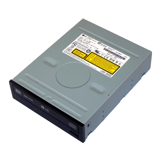
LOCATION OF CUSTOMER CONTROLS Front Panel Emergency Eject Hole Disc Tray Stop/Eject Button Drive Activity Indicators 1. Disc tray 3. Emergency Eject Hole This is the tray for the disc. Place the disc on the Insert a paper clip here to eject the Disc tray ejected disc tray, then lightly push the tray (or manually or when there is no power. -
Page 10: Rear Panel
Rear Panel IDE Interface Connector Analog Audio Output Connector Jumper Connector Power Connector Digital Audio Output Connector 1. Power Connector 3. Jumper Connector Connects to the power supply (5-and 12-V DC) of This jumper determines whether the drive is the host computer. configured as a master or slave. -
Page 11: Disassembly
DISASSEMBLY 1. CABINET and CIRCUIT BOARD 1-3. Cabinet and Main Circuit Board A. Remove the Cabinet in the direction of arrow (4). DISASSEMBLY (See Fig. 1-3) 1-1. Bottom Chassis B. Release 2 hooks (a) and remove the CD Tray A. Release 4 screws (A) and remove the Bottom Chassis drawing forward. -
Page 12: Pick-Up
2-2. Pick-up A. Release 1 screw (C) and remove the Pick-up. Pick-up Pick-up Unit Fig. 2-2... -
Page 13: Exploded View
EXPLODED VIEW PBM00 (MAIN C.B.A) - Page 14 GLOSSARY ATIP Absolute Time in Pre-groove. With an additional modulation of the “Wobble”, the “Groove” contains a time code information. Wobble The pre-groove in the Disc is not a perfect spiral but is wobbled. With : – A typical amplitude of 30 nm –...
-
Page 15: The Differences Of Cd-R/Cd-Rw Discs And General Cd-Rom
The differences of CD-R/CD-RW discs and General CD-ROM 1. Recording Layer Recordable CD has a wobbled pre-groove on the surface of disc for laser beam to follow track. Track pitch(p) a=30nm Read-only Disc CD-ROM (READ-ONLY DISC) Radial Direction Radial Error Signal 0.4~0.5 um Groove Land... -
Page 16: Disc Materials
3. Disc Materials 1) CD-ROM disc • It is composed of Silver _ colored aluminum plate and Reflective layer. • Groove (Pit) of aluminum plate make a track. • Laser wavelength : 780 nm, Laser Power (Read): 0.5mW • Signal is detected by the difference of reflective beam intensity between “pit”... -
Page 17: Reading Process Of Optical Disc
3) CD-RW Disc Label Printing Protective Layer Dielectric Layer(TL) Recording Layer Dielectric Layer(UL) Substrate (Polycarbonate) Groove Laser Beam • It is composed of polycarbonate layer, alloy(silver, arsenic) layer, aluminum reflectivity layer, protective layer. • An crystalized alloy layer is transformed into noncrystalized by the laser heat. Therefore, writing and reading is enabled by the difference of reflectivity. -
Page 18: Writing Process Of Cd-R Disc
5. Writing Process of CD-R Disc Incident (Write) Laser Power (Read) (Read) Laser Spot a b c d e f Position (Time) Laser Below "ORP"– Mark Too Short Spot Reflected At Optimum Record Power ("ORP") Light Signal Above "ORP" – Mark Too Long Recorded Mark Time... -
Page 19: Organization Of The Pca, Pma And Lead-In Area
7. Organization of the PCA, PMA and Lead-in Area 1) Layout of CD-ROM disc Disc Center Diameter 120 mm Diameter 46 mm Diameter 15 mm Center hole Clamping and Label Area Information Area Read Only Disc Lead-in Area Program Area Lead-out Area 2) Layout of CD-R/RW disc Disc Center... -
Page 20: Function Of Pca And Pma Area
8. Function of PCA and PMA area 1) PCA (Power Calibration Area) • PCA area is used to determine the correct Laser Power for a disc. – Method 1 : PCA area is divided by a track. – Method 2 : The previous Calibration value is referred. –... -
Page 21: Writing Process Of Disc
2) ROPC (Running Optimum Power Control) • Variable primary factor of Optimum Power – Change of Power sensitivity on the Disc. (limited to 0.05 *Po) – Wavelength shift of the laser diode due to the operating temperature change. – Change of the Spot aberration due to the Disc skew, Substrate thickness, Defocus. -
Page 22: The Differences Of Dvd-R/Rw, Dvd+R/Rw Discs And Dvdd-Rom
The differences of DVD-R/RW, DVD+R/RW discs and DVD-ROM 1. Recording Layer DVD-ROM (Read Only Disc) 0.4 um DVD-R/RW Disc (Land Pre-Pit) DVD+R/RW Disc... -
Page 23: Disc Specification
2. Disc Specification DVD-ROM DVD-R DVD-RW DVD+R DVD+RW Single-Layer Dual-Layer Media Type Read Only Read Only Phase change Phase change User data capacity 4.7GB 8.54GB 4.7GB 4.7GB 4.7GB 4.7GB Wavelength 650nm 650nm 650nm 650nm 650nm 650nm Reflectivity 45~85% 18~30nm 45~85% 18~30% 45~85% 18~30nm... - Page 24 2) Recording format using organic dye material (DVD-R/DVD+R) * The format that records data through the creation of recorded marks by changing the organic dye material with a laser beam. > Disc structure DVD-R DVD+R Adhesive layer Adhesive layer Protective layer Protective layer Reflective layer Reflective layer...
- Page 25 3) Recording format using phase-change recording material (DVD-RW/DVD+RW) * Data is recorded by changing the recording layer from the amorphous status to the crystalline status, and played back by reading the difference of the reflection coefficient. [ Amorphous : Non-crystalline ] >...
-
Page 26: Writing Pulse Waveform Of Dvd+R
4. Writing Pulse Wave Form of DVD+R For different speed ranges, different write strategies can be used. This document specifies 2 options: - a pulsed write strategy, where each single mark is created by a number of subsequent separated short pulses. - Page 27 2) 2 Method : Using Blocked Write Strategy NRZI Channel bits 1.25T top,3 1.25T 3T mark top,3 top,4 1.25T 4T mark top,4 1.25T 5T mark top,4 1.25T Etc. top,4 N = 3 : T (cm = 3) can be optimized individually. N >...
-
Page 28: Writing Pulse Waveform Dvd+Rw
5. Writing Pulse Wave Form of DVD+RW NRZI Channel bits Ttop dTera dTtop Pp : Actual write power Pe : Erase Power Pb : Bias Power... -
Page 29: Organization Of Inner Drive Area, Outer Drive Area, Lead-In Zone And Lead-Out Zone
6. Organization of the Inner Drive Area, Outer Drive Area, Lead-in Zone and Lead-out Zone 1) Layout of DVD-ROM disc Disc Center Diameter 120 mm Diameter 44 mm Diameter 33 mm Diameter 22 mm Diameter 16 mm Diameter 15 mm Clamping Center 3rd transtion... - Page 30 3) Layout of DVD+RW disc Disc Center Diameter 120 mm Diameter 44 mm Diameter 33 mm Diameter 22 mm Diameter 16 mm Diameter 15 mm Clamping Center 3rd transtion Information Zone Zone hole area 1st transition area Rim area 2nd transition area Unrecorded Disc Lead -out Zone Lead-in Zone...
-
Page 31: Dvd & Cd Data Processing
DVD & CD DATA PROCESSING 1. Data Processing Flow... -
Page 32: Copy Protection And Regional Code Management Block
2. Copy Protection and Regional Code Management Block Block Diagram Change the "KEY" HOST DVD HD62604FDV/BPV PLAYER (EMPEG2 B/D) Scrambled MPEG Data KEY Management Control Brief Process 1. Regional Code for DVD Disc – DVD-ROM drive transfers the regional code of the control data to host by the command of host, the DVD player of host reads the regional code, and plays title in the case of allowed regional code only. -
Page 33: About Prevention The Dvd-Rom From To Be Copy
3. About Prevention the DVD-ROM from to be copy A data is able to encode and record in the disc, if a copyright holder wants to prevent the disc from copying. In case of a disc enhanced movie of 3 titles..DISC KEY (2048 Bytes) is used to encode the whole contents in the disc and TITLE KEY (5 Bytes) is used to encode the title respectively. -
Page 34: About The Dvd-Rom Regional Code
4. About the DVD-ROM Regional Code Regional code U.S.A PRI. VIR DISC ROM - DRIVE MPEG-2 BOARD VGA CARD MONITOR Transfer to Receiving If the board is setting to the regional The disc has MPEG-2 board data from the code 1 for the U.S.A..the regional reading the MPEG-2... -
Page 35: Internal Structure Of The Pick-Up
INTERNAL STRUCTURE OF THE PICK-UP 1. Block Diagram of the PICK-UP(HOP-8511T) LM20BIM7 MON1 Rfreg SCLK IAPC SDIO ISLOP AGND BUSY RSET CP2860 NJM12984... -
Page 36: Pick Up Pin Assignment
2. Pick up Pin Assignment * Connector left side is no.1 and right side is no.54. Signal Name Signal Description Clock for NRZ code input. CLKB LVDS NRZ laser data (H=mark, L=space) NRZB NRZ laser data (L=mark, H=space) LDD GND ground connection SCLK Serial control clock... -
Page 37: Signal Detection Of The P/U
3. Signal detection of the P/U Infrared Iaser Pick-Up module Focusing Tracking Photo Diode 1) Focus Error Signal ==> (A+C)-(B+D) This signal is generated in RF IC (IC101 : HD15372TF) and controls the pick-up’s up and down to focus on Disc. 2) Tracking Error Signal (DPP Method) ==>... -
Page 38: Description Of Circuit
DESCRIPTION OF CIRCUIT 1. ALPC (Automatic Laser Power Control) Circuit 1-1. Block Diagram... - Page 39 1-2. ALPC (Automatic Laser Power Control) Circuit ALPC function DVD/CD anlaog front-end IC(IC101 HD153721TF) is for constant power control purpose. Based on the accurate power sensor(FMON) in P/U, ALPC feedback loop maintains constant power level against laser diode’s temperature variation. The ALPC loop amplifies(10x) the FMON signal to enhance the accuracy of read power level control.
-
Page 40: Focus Circuit
2. Focus Circuit 2-1. Block Diagram DVD : A1+A2+A3+A4 CD : EF1+EF2+EF3+EF4 (EF1~EF4) HAVC A1~A4 0.8V IC101 HD153721U HAVC B1~B4 (EF1~EF4) R701 Disc DVD : (B1+B3)-(B2+B4) Optical CD : (EF1+EF3)-(EF2+EF4) Motor unit Pick-up C703 HOP-8511T Focusing Compensator IC701 FACT- FACT+ HD62604 FCIN R625... -
Page 41: Tracking & Sled Circuit
3. Tracking & Sled Circuit 3-1-1. Block Diagram (Tracking Following) IC101 HD153721 MPPO (A+D)-(B+C) HAVC SPPO A1~A4 (F, E) DVD : (A1+A4)-(A2+A3) Disc R706 Optical CD : (EF1+EF2)-(EF3+EF4)-K*(E-F) Motor unit Pick-up HOP-8511T C708 Tracking Compensator TACT- TACT+ IC701 Sled Compensator HD62604 R630 ENC1... - Page 42 3-1-2. Block Diagram (Seek) IC101 HD153721 MPPO (A+D)-(B+C) (EF1~EF4) HAVC SPPO A1~A4 (F, E) K*{(F+H)-(E+G)} Disc Optical VREF1 C102 Motor unit Pick-up (A+D)-(B+C) HOP-8511T TEIN K*{(F+H)-(E+G)} VREF1 TACT- TACT+ HAVC MIRR MIRR SUMF BOTTOM HOLD HOLD RFIP SLED MOTOR Unit MIRRTOPH MIRRBOTH C118...
- Page 43 3-2-1. Tracking Servo The aim of tracking servo is to make laser beam trace the data track on disc. Tracking Error(TE) Signal is generated from tracking error detected block in HD153721 using DPP(Differential Push-Pull) Method(CD) and PP(Push-Pull) Method(DVD). DPP Method uses not only main beam(EF1~EF4) but also side beam(E, F) for correcting DC offset generated in Push-Pull Method.
-
Page 44: Spindle Circuit
4. Spindle Circuit 4-1-1. Block Diagram(FGCAV Servo) Optical Pick-up HOP-8511T Disc Motor unit X702 33.8688MHz IC701 XTALO VCK4M Control Clock HD62604 XTALI Generator SPIN CAV FD CAV PD VCK4M R610 R854 C606 Motor Kick 3.3V SPIN IC601 SPIN BD7905 1.65 CTL1 MUTE2 C602... - Page 45 4-2-1. Block Diagram (Wobble CLV Servo) C107 C108 C109 WAG1 WAG2 WAG3 21 22 AGC1 AGC2 Disc Motor uni t Optical Pick-up AGC3 HOP-8511T WOBSIG WBLSH IC101 WBLSH VREF HD153721TF IC701 HD62604 C606 R610 Motor Kick 4-2-2. Wobble CLV Servo DVD-RAM: 2x, 3x / DVD-R: 4x, 2x, 1x / DVD+R: 4x, 2.4x / DVD-RW: 1x, 2x / DVD+RW: 2.4x / CD-R 4x, 8x, 12x, 16x, 20x, 24x / CD-RW: 4x, 8x, 12, 16x When drive write DVD-RAM/R/RW/+R/+RW/CD-R/CD-RW, the spindle motor is controlled using Wobble CLV...
-
Page 46: Major Ic Internal Block Diagram And Pin Description
MAJOR IC INTERNAL BLOCK DIAGRAM AND PIN DESCRIPTION IC101 (HD153721TF) : RF AMP Analog Signal Processor Pin Assignment SUMF MCLK SUMF2 IP1/LPPOUT RFIP IP2/MIRR RFIN WOBSIG IREFT RDGATE VREF1 LO_ZB/SPDSH VCC2 IDGATE HAVC RFHLD/TISH1 HAVC2 BLANK HD153721TF SRVREF RECD1 PWDETO (TOP VIEW) GND4 RLDON... - Page 47 Block Diagram RF system power RF system power 0.1u 3300p VREF1 1500p 3900p (*2) *3300p/0.068u 4700p mclk ATEST 0.068u RFIP MIRR, DEFECT RF SUM/SUB RFIN EQOP AUTO (RGA) 0.068u SUMF EQON SUBP,N 0.068u IP1/LPPOUT EQOS/RRF/WRF IP2/MIRR mclk 15,000p SUBO/LPPMON SUBW SUBI /LPPSIG mclk 2200p...
- Page 48 • Pin Description Pin no. Pin Name Type Function LPS-A Analog-Output Lens shift signal output port. LPS-B Analog-Output Lens shift signal output port. Analog-Output Focus error output port. Analog-Output PE output. Analog-Output Tracking error output port. WRFIN Analog-Input WRF signal input port. TEIN Analog-Input TZC detection TE signal input port.
- Page 49 Pin no. Pin Name Type Function RLDON Digital-Input APC Read laser driver output control. GND4 Ground Ground[digital]. Digital-Output Tracking zero cross signal digital output port. PWDETO Digital-Output Laser diode over power detection output port. RECD1 Digital-Output Write/non-write detection output port. BLANK Digital-Output Write/non-write detection output port/BD detection...
- Page 50 Pin no. Pin Name Type Function EQON Differential-Output RF Equalizer differential output port. EQOP Differential-Output RF Equalizer differential output port. EQOS/RRF/WRF Analog-Output RF Equalizer single output port. RQHPF External-capacitor required AGC-DET input high path filter capacity connecting port. VCC1 Power Power.
- Page 51 IC701 (HD62604FDV) : Encoder, Decoder & DSP Singal Processor 1.1 Pin Layout ZIORB SCLK RFDEN ZIOWB DREQ WDEN UDBUSY DATA15 VCCIO VSSIO TRDP DATA0 TRDN DATA14 TLDP DATA1 VCCIO TLDN VSSIO DATA13 DATA2 FODP DATA12 FODN ENC1 VSSIO DATA3 ENC2 DATA11 TVDP DATA4...
- Page 52 1.2 Block Diagram VREF BIAS VREF33 VIBIAS LOUT EFMP AUDIO ROUT AUDIO EFMN Data DOUT DFF[1:0] Slicer JFF[1:0] DREQ CD-ROM DACK DCLPF[2:0] Decoder DASPB Descramble Data DRLPF[2:0] CS3FXB Strobe VISTRB CS1FXB R1CLPF PDIAG R1RLPF Ref-PLL CD-DSP R2CLPF[2:0] Jitter ATAPI R2RLPF[2:0] Counter Scramble VIREF[1:2]...
- Page 53 1.3 Pin Table Pin No. Ball Pin Name Ball Pin Name Ball Pin Name Ball Pin Name SCLK VREFC IDGATE RFDEN LPSAGT VSSA RFHLD WDEN LPSB VIREF1 IP1LPPIN LDBUSY TCPH VCCA IP2MIRR VCCIO R1CLPF VCCIO VSSIO VSSA R1RLPF VSSIO TRDP R2CLPF0 WRGATEB TRDN...
- Page 54 Pin No. Ball Pin Name Ball Pin Name Ball Pin Name Ball Pin Name DOUT IORDY DCKE MRSTB DACKB DRASB STANDBYB HRSTB HINTRQ VSSIO IOCS16B ADGATEB VCCIO RAMCLK INT0B DATA7 VSSIO VCCIO INT1B DATA8 VCCIO VSSIO INT2B DATA6 PDIAGB DCASB CPWRB VSSIO DQMU...
- Page 55 1.4 Pin Function It corresponds to the following signs as a pin I/O specification. AI : Analog Input IOU : Standard Input/Output with Pull Up AO : Analog Output 5I : 5V Tolerant Input AIO : Analog Input/Output 5O : 5V Tolerant Output Standard Input 5TO : 5V Tolerant Three State Output...
- Page 56 1.4.2 Servo Pin List Pin Name Destination Function Pin No. Ball No. Focus Error Input Pin Tracking Error Input Pin LPSAGT Lens Positioning A & GT Signal Input Pin PE Signal Input Pin External Focus Shock Signal Input Pin Components External Tracking Shock Signal Input Pin Components...
- Page 57 1.4.3 DRAM Interface Pin list Pin Name Destination Function Pin No. Ball No. RA[13:0] 224,222, 10A,11D, DRAM DRAM Address 223,220, 11A,11C, 221,219, 11C,12A, 215,213, 13A,14A, 211,209, 13B,15A, 210,212, 14D,13C, 214,216 13D,12C RD[15:0] 254,252, 4C,5B, DRAM DRAM Data 248,246, 3A,6B, 244,242, 4B,7B, 238,236, 6A,8B,...
- Page 58 1.4.4 ATAPI Interface Pin List Pin Name Destination Function Pin No. Ball No. HRSTB ATAPI ATA Drive reset ATAPI ATA Address DATA[15:0] 189,185, 18E,19D, ATAPI ATA Data 181,179, 17E,18F, 176,172, 20E,19H 170,167, 20G,18J, 166,168, 20H,19J, 171,175, 18H,18G, 177,180, 17F,20D, 184,186 20C,20B CS1FXB ATAPI...
- Page 59 1.4.5 Encoder Interface Pin List Pin Name Destination Function Pin No. Ball No. WRGATE2 Write Control Signal Output Pin for AFE WBLSH Wobble signal sampling pulse MPDSH Main beam sampling pulse WFPDSH The sampling pulse for laser control RFPDSH The sampling pulse for laser control TCSHSPBLV The terminal of a VFO1 track center signal sample / hold pulse it can change TCSH (VFO1 track...
- Page 60 1.4.6 Serial Communication Interface Pin List Pin Name Destination Function Pin No. Ball No. SDATA IF serial data for RF,LDD SCLK IF serial transmission clock for RF,LDD RFDEN IF transmission signal for RF WDEN IF transmission signal for LDD LDBUSY IF transmission busy signal for LDD 1.4.7 Audio Interface Pin List...
- Page 61 1.4.10 LSI/TEST Control Pin List Pin Name Destination Function Pin No. Ball No. MRSTB LSI master reset STANDBYB LSI analog module standby TESTB When it is made TEST mode selection TESTB=LOW, TMON [3:0] serves as a test control input terminal. Therefore, please do not usually set this terminal to Active at the time of operation.
- Page 62 1.4.11 Power Pin List Pin Name Destination Function Pin No. Ball No. VCCIO 5,81, 2E,6Y, Power supply (for Digital I/O 3.3V) 101,151, 12U20N, 165,174, 17J,20F, 183,199, 17D,18A, 217,230, 12B,8A, 240,250 5A,2A VCCA Power supply (for Servo ADC/DAC Block 3.3V) for DPLL Block 3.3V for SLICE Block 3.3V for RPLL1&BIAS Block 3.3V for RPLL2 Block 3.3V...
- Page 63 IC601 (BD7905BFS) : CD-ROM/DVD-ROM 6CH ACTUATOR DRIVER Block Diagram LEVEL LEVEL LEVEL SHIFT SHIFT SHIFT LOGIC LOGIC 117.5k 117.5k LIMIT LIMIT Current LIMIT Polarity REVERSE COMP DETECT 188k PRE LOGIC 112.5k STBY/ HALL BRAKE BIAS CONTROL Pin Description No Pin name Function No Pin name Function HU+ signal input SLIN1...
- Page 64 Input/Output circuit diagram Three-phase motor driver output Spindle driver current detection input Hall bias 54pin 51pin 312.5 8 17 Splindle driver feedback filter pin FG signal output Hall signal input 54pin 54pin 54pin 54pin 54pin PWM driver output SLED1, 2 BTL driver output FO, TK BTL driver output LD 31 32...
- Page 65 IC801 (µPD703101AGJ) : Microprocessor Pin Assignment INTP103/D MARQ3 / P07 A16/ P60 INTP102/D MARQ2 / P06 A17/ P61 INTP101/D MARQ1 / P05 A18/ P62 INTP100/D MARQ0 / P04 A19/ P63 TI10/P03 A20/ P64 TCLR10/P02 A21/ P65 TO101/P01 A22/ P66 TO100/P00 A23/ P67 IN TP113/DMAAK3/P17 CS0/RAS0/ P80...
- Page 66 Block Diagram HLDRQ HLDAK INTP10 0- I NTP103, INTC INTP110- I NTP113, CS0-CS7/RAS0/RAS7 INTP120- I NTP123, IOWR Command INTP130- I NTP133, IORD INTP140- I NTP143, INTP150- I NTP153 REFRQ Main DRAMC Multiplexer BCYST TO100, T O101, TO110, T O111, Parrel TO120, T O121, PAGE Shifter...
- Page 67 • Pin Description A0-A23 : Address Bus P50-P57 : Port 5 ADTRG : A/D Trigger Input P60-P67 : Port 6 ANI0-ANI7 : Analog Input P70-P77 : Port 7 : Analog Power Supply P80-P87 : Port 8 : Analog Reference Voltage P90-P97 : Port 9 : Analog Ground...
- Page 68 Pin Assignment Pin no. Pin name I/O Setting Symbol Description SFG interruption demand INT1 DSP interruption demand (RAM CTL/SRV system) INT2 DSP interruption demand (ATAPI system) INT0 DSP interruption demand (DSP) FM_SW Front monitor signal substitution Blank port Blank port AMUTE Audio Mute signal EJECTSW...
- Page 69 Pin no. Pin name I/O Setting Symbol Description XSCK0 Serial clock output Blank port Blank port Blank port +3.3V LDIN Loader in sensor LDOUT Loader out sensor DRVTMUTEB Tilt Driver Control Blank port Blank port Blank port Blank port Blank port Blank port P117 Blank port...
- Page 70 Pin no. Pin name I/O Setting Symbol Description P120 Blank port (CLKOUT) For Bus evaluation Blank port Blank port EEPRCE EEPROM Chip Select Blank port DSLADJ2 DSL Adjustment/EQ Boost Filter change single (XBCYST) For Bus evaluation DSLADJ Encoder output Loop Back Mute signal Read Strobe Blank port XLWR...
- Page 71 Pin no. Pin name I/O Setting Symbol Description Address Bus 4 Address Bus 3 Address Bus 2 Address Bus 1 Address Bus 0 HVdd +3.3V Data Bus 15 Data Bus 14 Data Bus 13 Data Bus 12 Data Bus 11 Data Bus 10 Data Bus 9 Data Bus 8...
-
Page 72: Troubleshooting Guide
TROUBLESHOOTING GUIDE ADJUST BLOCK DIAGRAM (01) Laser Power Adjust (using RD Power/WR Power/Erase Power) IC701 IC801 Pickup Setting Pin#27 pin#28 Front Monitor Driver IC101 IC103 IC104 IC105 (02) High Frequency Adjust Pickup Setting 45-49 IC801 Driver IC701 (03) Data Slice/Equalizer Boost/Raw Slice/ Equalizer Frequency Adjust Setting Pin#77 IC701... - Page 73 (06) Focus Amp. Adjust for DVD-Dual DVD-Dual Disc Setting Pin# Setting Pickup 86-98 IC801 FE:R701,R740 IC101 C703 (Signal Amp) IC701 Focus:#45-46 R625, Slider FPC Driver C628 Slider:#34-37 IC601 (07) Focus Amp. and Total Amp. Adjust All Disc Setting Pin# Setting Pickup 86-98 IC101...
- Page 74 (10) Servo Loop Gain Adjust All Disc Pin# Setting Pickup Setting 86-98 IC101 IC801 FE:R701,R740 C703 IC701 TE:R706,R741 Focus:#45-46 C708 Tracking:#47-48 R625, C628 #53 Driver Slider FPC IC601 Slider:#34-37 R624, C627 #52 DVD-RAM Disc (11) Unwritten Slice Level Adjust for DVD-RAM Pin# Setting Setting...
- Page 75 (14) Focus Offset Adjust for DVD-RAM (Data Error Pulse) DVD-RAM Disc Pin# Setting Setting 86-98,78-79 IC101 IC801 IC701 Pickup C727,728 (PI Error) #68,69 Slider FPC Driver Slider:#34-37 IC601 (15) Tilt Adjust for DVD-RAM DVD-RAM Disc Pin# Setting Setting Pickup 86-98,78-79 IC101 IC801 TCPH:R709,C711...
- Page 76 (18) Focus Offset Adjust for DVD-R/RW, DVD+R/RW, CD-R/RW DVD-R/RW Disc Setting Pin# Setting 86-98,78-79 IC801 TE:R706,R741 IC101 Pickup IC701 C708 (Tracking Amp) TE:#47-48 Driver TE:R624, C627 Slider FPC IC601 Slider:#34-37 (19) Lens Sensitivity Adjust Setting Pickup IC801 (Temp.Information) (20) Spindle Offset Adjust Pin# Setting Spindle...
- Page 77 (23) RTZ TimeOut Fail Setting Setting Driver IC602 #2,13 IC701 IC801 Slider/ R630, Spindle R635 #28-29 Slider FPC Driver Slider:#34-37 IC601 Spindle FFC (24) Focus Servo/Tracking Servo Fail All Disc Setting Pin# Setting 86-98 IC101 IC801 FE:R701,R740 C703 Pickup IC701 TE:R706,R741 C708 Focus:#47-46...
- Page 78 Detail Error Code & Fail Analysis 1. Laser Power Initial Adjust Error Code Contents of fail Fail Analysis Block Diagram SSB Byte8,9 28xx LP Adjust NG. 1) Check Pickup FFC Connection. No.01 (Exchange 2) Check solder of IC101circumference. low/high byte) (pin#10, 14, 16, L101, L103) 3) Check solder of IC103,IC104,IC105.
- Page 79 2. Adjusting Error during Disc Load Sequence (Lead in Error) No. Error Code Contents of fail Fail Analysis Block Diagram SSB Byte21,22 42xx Circuit Offset Adjust NG. 1) Check Pickup FFC Connection. No.04 2) Check solder of IC101circumference . (pin#3,4,5 pin#86-98, FE_Servo: R701, R740, C703 TE_Servo: R706, R741, C708 PE_Servo: R702, C704)
- Page 80 No. Error Code Contents of fail Fail Analysis Block Diagram SSB Byte21,22 46xx Lens Position Adjust NG. 1) Check Pickup FFC Connection. No.09 2) Exchange Pickup. 3) Check solder of IC101circumference. (pin#3,4,5 pin#86-98, TE_Servo: R706, R741, C708) 4) Check solder of IC701circumference. (R707,R708,C709,C710) 5) Exchange IC508.
- Page 81 No. Error Code Contents of fail Fail Analysis Block Diagram SSB Byte21,22 4Cxx Data Slice Adjust NG. 4C88/4C89: RAM Disc NG No.14 (RAM Only) (Excahnge RAM Disc). 2) Exchange Pickup. 3) Exchange IC101(AFE). 4) Exchange IC701(DSP). 4Dxx Focus Deviation Adjust NG. 1) Check Pickup FFC Connection.
- Page 82 No. Error Code Contents of fail Fail Analysis Block Diagram SSB Byte21,22 57xx HFPE Amp/Gain Adjust NG. 1) Check Pickup FFC Connection. No.15 2) Exchange Pickup. 3) Check solder of IC101circumference. (pin#10,11 R709,C711,R704,C706) 4) Exchange IC101(AFE). 5) Exchange IC701(DSP). 58xx Lens Sensitivity Adjust NG.
- Page 83 3. Loading Sequence Error (Lead in Error) No. Error Code Contents of fail Fail Analysis Block Diagram SSB Byte21,22 2503,2504 RTZ Timeout(Sled Timeout). 1) Check Slider FPC Connection. No.23 2) Check solder of IC601 circumference . (pin#28-29, 34-37) 3) Check solder of IC602 circumference. (pin#2,13 R630, R635, C618, C619) 4) Exchange Slider Motor.
- Page 84 Power Supply System Diagram 6ch_DRIVE(SPDL,SLED,LOAD)_VM_12V P_RESET(IC506) R separation L501 5AREG R513 L502 SW_reg pick_up VSO_4.2V (PDD) Line-in : 12V TH501 IC501 L102 pick_up VSA_5.0V (LDO) pick_up AVCC_5.0V(OEIC) Tr_SW L506 STANBYON OP-amp_5.0V(Vref) L104 HD153721_VCC4_5.0V digital L101 HD153721_VCC_5.0V analog OP-amp_5.0V(APC) AUDIO_amp_5.0V Tilt_DRIVE_VM_5V 6ch_DRIVE(Fo,Tr)_VM_5V &...
- Page 85 PCB Poor Analysis - Check list Circuit/IC Signal Signal/Level mesurement-point (IC-pin or Device) Power supply Line-12V PG901-56 Line-5V PG901-53 (IC501) reg-5.0V L502 (IC504) reg-3.3V 3.3V (IC505) reg-1.5V 1.5V VDD : 3.3V 3.3V 45, 62, 100, 126, 144 (IC801) Clock-5MHz 5.0MHz 63, 64 PSRST 3.3V(High)
- Page 86 HW Self- Diagnostic function 1. Self-Diagnostic Function by LED Blink. • Basic operation: MPU accesses each peripheral (inside, exterior) device, and discover a defect by the ability of a read/write of data to be performed correctly. Since MPU operates by the program with a built-in Flash-ROM, when abnormalities are in MPU, Flash-ROM, and these Data-Bus &...
- Page 87 2. LED does not blink at all at the time of a power supply injection. Eject-SW does not react. (1) Is it normal to the exterior Bus (Data-Bus, Address-Bus, control signal system) of MPU? Viewing — check: -- a short circuit, opening, etc. •...
- Page 88 3. Motor, Abnormalities in Actuator System The drive circuit of a motor & actuator consists of the three ICs IC601 (BD7905BFS), IC603 (BA5962FVM) and IC602 (BU2507FV). The work of each IC is as follows. (1) IC601(BD7905BFS) : 6ch driver Spindle motor driver: 180 degree electronically Type, an analog input, a PWM drive, a Vm=12V. Stepping motor driver X2: analog input, a PWM drive (differential), a Vm=12V Loading motor driver: analog input / output (differential), a Vm=12V Focus actuator driver: analog input / output (differential), a Vm=5V...
-
Page 89: Block Diagram
BLOCK DIAGRAM Headphones BUFFER RAM Jack (2MByte) K4S1616220 or Equivalent OPU:HOP-8511T (SAMSUNG) (HITACH ME) Disc Interface Loading motor DVD/CD DSP connector Front End LSI (DVD/CD/Servo/AT API) HD62604FDV HD153721TF Analog 256pin LQFP 100pin-TQFP audio Disc (HITACHI) Slide motor (HITACHI) motor Unit DVD-codec mechanism CD-codec...
Need help?
Do you have a question about the GSA-4040B and is the answer not in the manual?
Questions and answers