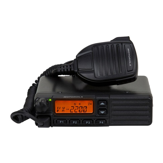
Vertex Standard VX-2200 Series Service Manual
Uhf fm transceiver
Hide thumbs
Also See for VX-2200 Series:
- Service manual (84 pages) ,
- Operating manual (33 pages) ,
- Operating manua (21 pages)
Table of Contents
Advertisement
Quick Links
UHF FM Transceiver
VX-2100 Series
VX-2200 Series
Service Manual
©
2008 VERTEX STANDARD CO., LTD.
VX-2100 Series
Introduction
This manual provides the technical information necessary for servicing the VX-2100/-2200 Series Mobile Transceiver.
Servicing this equipment requires expertise in handing surface-mount chip components. Attempts by non-qualified
persons to service this equipment may result in permanent damage not covered by the warranty, and may be illegal
in some countries.
Two PCB layout diagrams are provided for each double-sided board in this transceiver. Each side of the board is
referred to by the type of the majority of components installed on that side ("Side A" or "Side B"). In most cases one
side has only chip components (surface-mount devices), and the other has either a mixture of both chip and leaded
components (trimmers, coils, electrolytic capacitors, ICs, etc.), or leaded components only.
As described in the pages to follow, the advanced microprocessor design of the VX-2100/-2200 allows a complete
Alignment of this transceiver to be performed without opening the case of the radio; all adjustments can be performed
from the personal computer, using with the Vertex Standard VPL-1 Programming Cable and CE82 Software.
While we believe the information in this manual to be correct, Vertex Standard assumes no liability for damage that
may occur as a result of typographical or other errors that may be present. Your cooperation in pointing out any
inconsistencies in the technical information would be appreciated.
This transceiver was assembled using Pb (lead) free solder, based on the RoHS specification.
Only lead-free solder (Alloy Composition: Sn-3.0Ag-0.5Cu) should be used for repairs performed on this ap-
paratus. The solder stated above utilizes the alloy composition required for compliance with the lead-free
specification, and any solder with the above alloy composition may be used.
Specifications ........................................................... A-1
Dsub 15-Pin Accessory Connector ...................... B-1
Exploded View & Miscellaneous Parts ............... C-1
Block Diagram ......................................................... D-1
Circuit Description .................................................. E-1
Alignment ................................................................. F-1
Installation Of Option ............................................ G-1
EC061U90C
Important Note
Contents
Board Units (Schematics, Layouts & Parts)
Main Unit .......................................................... H-1
FRONT-A Unit ( VX-2100 ) ................................... I-1
FRONT-B Unit ( VX-2200 ) ................................... J-1
Optional Units (Schematics, Layouts & Parts)
FVP-25 Encryption/DTMF Pager Unit ............. K-1
FVP-36 Voice Inversion Type Encryption Unit ..... L-1
VERTEX STANDARD CO., LTD.
4-8-8 Nakameguro, Meguro-Ku, Tokyo 153-8644, Japan
VERTEX STANDARD
US Headquarters
10900 Walker Street, Cypress, CA 90630, U.S.A.
YAESU EUROPE B.V.
P.O. Box 75525, 1118 ZN Schiphol, The Netherlands
YAESU UK LTD.
Unit 12, Sun Valley Business Park, Winnall Close
Winchester, Hampshire, SO23 0LB, U.K.
VERTEX STANDARD HK LTD.
Unit 5, 20/F., Seaview Centre, 139-141 Hoi Bun Road,
Kwun Tong, Kowloon, Hong Kong
VX-2200 Series
Advertisement
Table of Contents

Related Manuals for Vertex Standard VX-2200 Series


Summary of Contents for Vertex Standard VX-2200 Series
- Page 1 Vertex Standard VPL-1 Programming Cable and CE82 Software. While we believe the information in this manual to be correct, Vertex Standard assumes no liability for damage that may occur as a result of typographical or other errors that may be present. Your cooperation in pointing out any inconsistencies in the technical information would be appreciated.
-
Page 2: Specifications
400 - 470 MHz (Type A) 450 - 512 MHz (VTX, Type D) 450 - 520 MHz (EXP, Type D) Number of Groups: 1 groups (VX-2100 Series) 8 groups (VX-2200 Series) Number of Channels: 8 channels (VX-2100 Series) 128 channels (VX-2200 Series) Power Supply Voltage: 13.6 V ±... - Page 3 Specifications (EU Version) General Frequency Ranges: 400 - 470 MHz Number of Groups: 1 groups (VX-2100 Series) 8 groups (VX-2200 Series) Number of Channels: 8 channels (VX-2100 Series) 128 channels (VX-2200 Series) Power Supply Voltage: 10.8 - 15.6 V DC Channel Spacing: 12.5 / 20 / 25 kHz...
-
Page 4: Dsub 15-Pin Accessory Connector
DSUB 15-pin Accessory Connector Pin 1: AF IN ( A Pin 6: EXT PTT NALOG NPUT External Microphone Input. Nominal input level is 6 Shorting this port to ground causes the transceiver to mV at 600-ohm. be placed in the Transmit mode, while opening the When connect the External Microphone to this port, connection to this port returns the transceiver to the insert a 0.1 µF coupling capacitor between the micro-... -
Page 5: Exploded View & Miscellaneous Parts
FRONT-B-UNIT CONNECTOR RA0790900 REFLECTOR SHEET RA079000A (Lot. 1-8) RA079000B (Lot. 9-) CHASSIS RA078640A LIGHT GUIDE G6090173 VX-2200 FRONT PANEL Non-designated parts are available only as RA080360A RA0786300 part of a designated assembly. RUBBER PACKING LCD HOLDER RA0786900 T9318284 SUPPLIED ACCESSORIES... - Page 6 Exploded View & Miscellaneous Parts Note:...
-
Page 7: Block Diagram
Block Diagram... - Page 8 Block Diagram Note:...
-
Page 9: Circuit Description
Circuit Description 1. Circuit Configuration by Frequency 2-4. Audio amplifier Detected signal from Q1036 (NJM2591V) is inputted to The receiver is a double-conversion superheterodyne with Q1042 (NJM12902V) and is output through the band pass a first intermediate frequency (IF) of 67.65 MHz and a filter inside Q1042 (NJM12902V). - Page 10 Circuit Description 3. Transmitter System 3-4-1. VCO While the radio is receiving, the RX oscillator Q1029 3-1. Mic Amplifier (2SK508) in the VCO generates a programmed frequency There are two micrphone inputs, J1004 (front) and J1006 (receive frequncy plus 67.65 MHz) as 1st local signal. (D-Sub).
-
Page 11: Alignment
Beacuse of the BTL (Bridged TransLess) Amplifier circuit pair and alignment. Therefore, if a fault is suspected, con- used in the VX-2200/-2100, do not connect eather side of tact the dealer from whom the transceiver was purchased the speaker leads to chassis “ground.”... - Page 12 The Alignment Tool Outline Installation the tool Install the CE82 (Clone Editor) to your PC. The re-alignment for VX-2200/-2100 series may use the “Alignment” menu of CE82. Action of the switches When the transceiver is in alignment mode, the action of PTT and KEY is ignored.
- Page 13 Alignment Unit During alignment, the values of dBµV or µV (EMF or PD) can be selected or dBm. 1. RX VCO Tune Voltage (RX VCO) This parameter is to align the “Tune Voltage” of RX VCO. This alignment will be done automatically between the radio and PC.
- Page 14 Alignment 3. PLL Reference Frequency (Frequency) This parameter is to align the reference frequency for PLL. The “TX VCO Tune Voltage” alignment must be done before this alignment is going to start. 1. Press the “Start” button to start the alignment then the radio will transmit on the center frequency.
- Page 15 Alignment RSSI SQL Full Scale <Wide> (S Full Scale W) The Alignment for the RSSI Full Scale level at Wide (5k/ 4k). Noise SQL Tight <Narrow> (TI NSQ N) The Alignment for the Noise SQL Tight level at Narrow (2.5k). Noise SQL Threshold <...
- Page 16 Alignment 7. Maximum Deviation <Wide> / <Narrow> This parameter is to align the Maximum Deviation (Wide/Narrow). The “TX VCO Tune Voltage” must be done before this alignment is started. 1. Press the “Start” button to start the alignment. 2. Set the value to get desired deviation (Wide: 4.2kHz, Narrow: 2.1kHz) on the deviation meter by changing the slide bar on your PC.
- Page 17 Alignment CH (Channel-by-Channel) Fine Alignment Mode The CH Fine Alignment Mode allows you to align the ra- dio separately for every operating channel. The value of each parameter can be changed to the desired position us- ing the “ ” / “ ” and up/down arrow keys, direct number input, and by dragging the PC mouse.
-
Page 18: Installation Of Option
Installation of Option FVP-25/FVP-35/FVP-36 The FVP-25 is an Encryption/DTMF Pageing Unit which 1. Disconnect the DC power cable. permits secure voice communications with station within 2. Referring to Figure 1, remove the 8 screws affixing the your network, while preventing others from listening us- Top Cover, then remove the top cover. -
Page 19: Main Unit
MAIN Unit (Lot 1~4) 67.65MHz RX:2.0V -108.5dBm RX:1.9V -86.0 dBm RX:7.6V -72.0 dBm RX:7.5V RX:8.1V RX:1.1V TX:0V -110.0dBm (C1198 removed) TX:0V -88.5 dBm (C1046 removed) TX:0V -76.5 dBm (C1146 removed) TX:0V TX:0V TX:0V 67.65MHz -73.5 dBm -42.5 dBm (C1230 removed) Circuit Diagram RX:4.5V RX:1.4V... - Page 20 MAIN Unit (Lot 1~4) Note...
- Page 21 MAIN Unit (Lot 1~4) Parts Layout (Side A) NJM7808DL1A (Q1006) BU4053BCFV (Q1004, 1005) MTM231230L (BL) (Q 1008, 1011, 1012) 2SK397300L (Q1050, 1055, 1060, 1063, 1070) RA45H4452M (Q1009) UMG2N (Q1013) M62364FP (Q1014) BH2220FVM LC87F5CC8A NJM12902V 2SB1201S-TL RT1N441U (N3) 3SK293 (UF) TAR5S35 (3V5) XN1501 (R5) TAR5S50 RT1N140U...
- Page 22 MAIN Unit (Lot 1~4) Parts Layout (Side B) DAN222 (N) (D1020, 1035, 1039) MC2850 (A7) (D1021, 1027, 1041 1046, 1047, 1048 1053, 1054) 2SC4617 (BR) (Q1018, 1019, 1020, BU4066BCFV-E2 TDA1519CTH ADF4111BRUZ-RL7 DTA124EE (15) DTC143EE (23) RT1N140U RT1N441U (N3) S-80835CNMC 2SC3357-T2 2SK508 (K52) 1032, 1056) (Q1044)
- Page 23 MAIN Unit (Lot 5~9) Circuit Diagram...
- Page 24 MAIN Unit (Lot 5~9) MAIN Unit...
- Page 25 MAIN Unit (Lot 5~9) Parts Layout (Side A) NJM7808DL1A (Q1006) BU4053BCFV (Q1004, 1005) MTM231230L (BL) (Q 1008, 1011, 1012) 2SK397300L (Q1050, 1055, 1060, 1063, 1070) RA45H4452M (Q1009) UMG2N (Q1013) M62364FP (Q1014) BH2220FVM LC87F5CC8A NJM12902V 2SB1201S-TL DTA124EE (15) RT1N441U (N3) 3SK293 (UF) TAR5S35 (3V5) XN1501 (R5) TAR5S50...
- Page 26 MAIN Unit (Lot 5~9) Parts Layout (Side B) DAN222 (N) (D1020, 1035, 1039) MC2850 (A7) (D1021, 1027, 1041 1046, 1047, 1048 1053, 1054) 2SC4617 (BR) (Q1018, 1019, 1020, BU4066BCFV-E2 TDA1519CTH LC73881M (USA; Lot. 7~) ADF4111BRUZ-RL7 DTA124EE (15) DTC143EE (23) RT1N140U RT1N441U (N3) S-80835CNMC 2SC3357-T2...
- Page 27 MAIN Unit (Lot 10~12) Circuit Diagram...
- Page 28 MAIN Unit (Lot 10~12) Note H-10...
- Page 29 MAIN Unit (Lot 10~12) Parts Layout (Side A) NJM7808DL1A (Q1006) BU4053BCFV (Q1004, 1005) MTM231230L (BL) (Q 1008, 1011, 1012) 2SK397300L (Q1050, 1055, 1060, 1063, 1070) S-AU83AL (25 W, Ver A) S-AU83AH (25 W, Ver D) RA55H4047M (45 W, Ver A) (Lot. 11~) RA45H4452M-24 (45 W, Ver D) (Q1009) UMG2N...
- Page 30 MAIN Unit (Lot 10~12) Parts Layout (Side B) DAN222 (N) (D1020, 1035, 1039) MC2850 (A7) (D1021, 1027, 1041 1046, 1047, 1048 1053, 1054) 2SC4617 (BR) (Q1018, 1019, 1020, BU4066BCFV-E2 TDA1519CTH ADF4111BRUZ-RL7 DTA124EE (15) DTC143EE (23) RT1N140U RT1N441U (N3) S-80835CNMC 2SC3357-T2 2SK508 (K52) 1032, 1056) (Q1044)
- Page 31 MAIN Unit (Lot 13~) Circuit Diagram H-13...
- Page 32 MAIN Unit (Lot 13~) Note H-14...
- Page 33 MAIN Unit (Lot 13~) Parts Layout (Side A) NJM7808DL1A (Q1006) BU4053BCFV (Q1004, 1005) MTM231230L (BL) (Q 1008, 1011, 1012) 2SK397300L (Q1050, 1055, 1060, 1063, 1070) S-AU83AL (25 W, Ver A) S-AU83AH (25 W, Ver D) RA55H4047M (45 W, Ver A) (Lot. 11~) RA45H4452M-24 (45 W, Ver D) (Q1009) UMG2N...
- Page 34 MAIN Unit (Lot 13~) Parts Layout (Side B) DAN222 (N) (D1020, 1035, 1039) MC2850 (A7) (Lot. 1~19) DAN217U (A7) (Lot. 20~) (D1021, 1027, 1041 1046, 1047, 1048 1053, 1054) 2SC4617 (BR) (Q1018, 1019, 1020, BU4066BCFV-E2 TDA1519CTH ADF4111BRUZ-RL7 DTA124EE (15) DTC143EE (23) RT1N140U (Lot.
-
Page 35: Main Unit
MAIN Unit Parts List DESCRIPTION VALUE TOL. MFR'S DESIG VXSTD P/N VERS. LOT SIDE LAY ADR PCB with Components CS1888002 EXP TYPE D 45 W CS1888003 VTX TYPE D 45 W CS1888005 CE TYPE A 25 W CS1888006 VTX TYPE D 25 W CS1888007 EXP TYPE D 25 W CS1888008... -
Page 36: Parts List
MAIN Unit Parts List DESCRIPTION VALUE TOL. MFR'S DESIG VXSTD P/N VERS. LOT SIDE LAY ADR C 1026 CHIP CAP. 33pF GRM1552C1H330JZ01D K22178224 C 1027 CHIP CAP. 100pF GRM1552C1H101JD01D K22178236 C 1028 CHIP CAP. 0.01uF GRM36B103K16PT K22128804 C 1028 CHIP CAP. 0.01uF GRM155B11E103KA01D K22148834... - Page 37 MAIN Unit Parts List DESCRIPTION VALUE TOL. MFR'S DESIG VXSTD P/N VERS. LOT SIDE LAY ADR C 1080 CHIP CAP. 100pF GRM1552C1H101JD01D K22178236 C 1081 CHIP CAP. 100pF GRM1552C1H101JD01D K22178236 C 1083 CHIP CAP. 220pF GRM36CH221J25PT K22148203 C 1083 CHIP CAP. 220pF GRM1552C1H221JA01D K22179713...
- Page 38 MAIN Unit Parts List DESCRIPTION VALUE TOL. MFR'S DESIG VXSTD P/N VERS. LOT SIDE LAY ADR C 1138 CHIP CAP. 100pF GRM1552C1H101JD01D K22178236 C 1139 CHIP CAP. 0.001uF GRM155B11H102KA01D K22178809 C 1139 CHIP CAP. 47pF GRM1552C1H470JZ01D K22178228 VERSION A 10- C 1139 CHIP CAP.
- Page 39 MAIN Unit Parts List DESCRIPTION VALUE TOL. MFR'S DESIG VXSTD P/N VERS. LOT SIDE LAY ADR C 1195 CHIP CAP. GRP1553C1H3R0CZ01E K22178205 VERSION D 10- C 1196 CHIP CAP. 0.0047uF GRM36B472K25PT K22148830 C 1196 CHIP CAP. 0.0047uF GRM155B11H472KA01D K22178838 C 1197 CHIP CAP.
- Page 40 MAIN Unit Parts List DESCRIPTION VALUE TOL. MFR'S DESIG VXSTD P/N VERS. LOT SIDE LAY ADR C 1259 CHIP CAP. 180pF GRM36CH181J25PT K22148201 C 1259 CHIP CAP. 180pF GRM1552C1H181JA01D K22179711 C 1260 CHIP CAP. 0.001uF GRM155B11H102KA01D K22178809 C 1261 CHIP CAP. 0.0033uF GRM155B11H332KA01D K22178815...
- Page 41 MAIN Unit Parts List DESCRIPTION VALUE TOL. MFR'S DESIG VXSTD P/N VERS. LOT SIDE LAY ADR C 1317 CHIP CAP. 0.01uF GRM155B11E103KA01D K22148834 C 1319 CHIP TA.CAP. 4.7uF TEESVA1C475M8R K78120031 C 1321 CHIP CAP. 0.001uF GRM155B11H102KA01D K22178809 C 1323 CHIP CAP. 100pF GRM1552C1H101JD01D K22178236...
- Page 42 MAIN Unit Parts List DESCRIPTION VALUE TOL. MFR'S DESIG VXSTD P/N VERS. LOT SIDE LAY ADR C 1390 CHIP CAP. GRM1554C1H2R0CZ01D K22178204 VERSION A 10- C 1391 CHIP CAP. GRM1552C1H9R0DZ01D K22178211 VERSION A 10- C 1391 CHIP CAP. GRM1552C1H5R0CZ01D K22178207 VERSION D 10- C 1393 CHIP CAP.
- Page 43 MAIN Unit Parts List DESCRIPTION VALUE TOL. MFR'S DESIG VXSTD P/N VERS. LOT SIDE LAY ADR D 1053 DIODE MC2850-T111-1 G2070704 D 1053 DIODE DAN217U T106 G2071236 D 1054 DIODE MC2850-T111-1 G2070704 D 1054 DIODE DAN217U T106 G2071236 D 1055 DIODE MAZ816000L G2071120...
- Page 44 MAIN Unit Parts List DESCRIPTION VALUE TOL. MFR'S DESIG VXSTD P/N VERS. LOT SIDE LAY ADR L 1023 M.RFC 0.082uH HK1608 82NJ-T L1690527 L 1024 M.RFC LK1608 1R0K-T L1690687 L 1025 M.RFC 0.39uH C1608CB-R39G-RF L1691107 L 1026 M.RFC 0.22uH HK1608 R22J-T L1690940 L 1027 COIL...
- Page 45 J24189033 R 1005 CHIP RES. 1/16W RMC1/16S 223JTH J24189041 R 1006 CHIP RES. 470k 1/16W RMC1/16S 474JTH J24189057 R 1007 CHIP RES. RMC1 101JTE J24305101 R 1008 CHIP RES. 470k 1/16W RMC1/16S 474JTH J24189057 : Please contact Vertex Standard H-27...
- Page 46 MAIN Unit Parts List DESCRIPTION VALUE TOL. MFR'S DESIG VXSTD P/N VERS. LOT SIDE LAY ADR R 1009 CHIP RES. 270k 1/16W RMC1/16S 274JTH J24189054 R 1010 CHIP RES. 100k 1/16W RMC1/16S 104JTH J24189049 R 1011 CHIP RES. 1/16W RMC1/16S 471JTH J24189021 R 1012 CHIP RES.
- Page 47 MAIN Unit Parts List DESCRIPTION VALUE TOL. MFR'S DESIG VXSTD P/N VERS. LOT SIDE LAY ADR R 1071 CHIP RES. 1/16W RMC1/16S 473JTH J24189045 R 1072 CHIP RES. 1/16W RMC1/16S 473JTH J24189045 R 1073 CHIP RES. 1/16W RMC1/16S 103JTH J24189037 R 1074 CHIP RES.
- Page 48 MAIN Unit Parts List DESCRIPTION VALUE TOL. MFR'S DESIG VXSTD P/N VERS. LOT SIDE LAY ADR R 1136 CHIP RES. 100k 1/16W RMC1/16S 104JTH J24189049 R 1137 CHIP RES. 1/16W RMC1/16S 101JTH J24189013 R 1138 CHIP RES. 1/16W RMC1/16S 102JTH J24189025 R 1139 CHIP RES.
- Page 49 MAIN Unit Parts List DESCRIPTION VALUE TOL. MFR'S DESIG VXSTD P/N VERS. LOT SIDE LAY ADR R 1194 CHIP RES. 1/16W RMC1/16S 823JTH J24189048 R 1195 CHIP RES. 1/16W RMC1/16S 220JTH J24189005 R 1196 CHIP RES. 1/16W RMC1/16S 473JTH J24189045 R 1198 CHIP RES.
- Page 50 MAIN Unit Parts List DESCRIPTION VALUE TOL. MFR'S DESIG VXSTD P/N VERS. LOT SIDE LAY ADR R 1277 CHIP RES. 1/16W RMC1/16S 220JTH J24189005 R 1279 CHIP RES. 1/16W RMC1/16S 102JTH J24189025 R 1280 CHIP RES. 1/16W RMC1/16 000JATP J24185000 R 1281 CHIP RES.
- Page 51 MAIN Unit Parts List DESCRIPTION VALUE TOL. MFR'S DESIG VXSTD P/N VERS. LOT SIDE LAY ADR R 1353 CHIP RES. 1/10W RMC1/10T 473J J24205473 R 1357 CHIP RES. 100k 1/16W RMC1/16S 104JTH J24189049 R 1358 CHIP RES. 1/16W RMC1/16S 102JTH J24189025 R 1359 CHIP RES.
- Page 52 MAIN Unit Note H-34...
-
Page 53: Front-A Unit ( Vx-2100 )
FRONT-A Unit (VX-2100) Circuit Diagram RX: 4.9V RX: 0V TX: 0V TX: 4.9V 5.0V 13.6V... - Page 54 FRONT-A Unit (VX-2100) Parts Layout (Side A) RT1N441U (N3) BRPG1211C (Q2011, 2013, 2014, 2015) (D2001) Parts Layout (Side B) RT1N441U (N3) CD4094BPWR UA78L05ACPK (F5) (Q2001, 2002, 2003, 2004, (Q2005, 2012) (Q2007) 2006, 2008, 2009, 2010)
- Page 55 FRONT-A Unit (VX-2100) Parts List DESCRIPTION VALUE TOL. MFR'S DESIG VXSTD P/N VERS. LOT SIDE LAY ADR PCB with Components CB3474001 Printed Circuit Board FR014510B C 2001 CHIP TA.CAP. 4.7uF TEESVB21E475M8R K78140019 C 2002 CHIP CAP. 0.1uF GRM21BB11E104KA01L K22140811 C 2003 CHIP CAP.
- Page 56 FRONT-A Unit (VX-2100) Note...
-
Page 57: Front-B Unit ( Vx-2200 )
FRONT-B Unit (VX-2200) Circuit Diagram RX: 4.9V TX: 0V RX: 0V TX: 4.9V DIMMER LEVEL 3: 4.8V 5.0V 5.0V... - Page 58 FRONT-B Unit (VX-2200) Parts Layout (Side A) BRPG1211C (D3005) (DS3001) Parts Layout (Side B) 2SB1132 (BA) XP1501 (R5) RT1N441U (N3) CD4094BPWR (Q3001) (Q3002, 3007) (Q3003, 3004) (Q3005) UA78L05ACPK (F5) 2SA1602A (MF) NJU6533KQ1 (Q3006) (Q3008) (Q3009)
- Page 59 FRONT-B Unit (VX-2200) Parts List DESCRIPTION VALUE TOL. MFR'S DESIG VXSTD P/N VERS. LOT SIDE LAY ADR PCB with Components CB3475001 Printed Circuit Board FR014520C C 3001 CHIP TA.CAP. 4.7uF TEESVB21E475M8R K78140019 C 3002 CHIP CAP. 0.1uF GRM21BB11E104KA01L K22140811 C 3003 CHIP CAP.
- Page 60 FRONT-B Unit (VX-2200) Note:...
-
Page 61: Fvp-25 Encryption/Dtmf Pager Unit
FVP-25 Encryption/DTMF Pager Unit (Option) Circuit Diagram Parts Layout Side A Side B M64026FP LC73881 DTC144EU (26) (Q1001) (Q1002) (Q1003) - Page 62 FVP-25 Encryption/DTMF Pager Unit (Option) Parts List DESCRIPTION VALUE TOL. MFR'S DESIG VXSTD P/N VERS. LOT SIDE LAY ADR Printed Circuit Board FR005010F C 1001 CHIP CAP. 0.1uF GRM188B11C104KA01D K22124805 C 1002 CHIP CAP. 0.01uF GRM39B103M25PT K22144802 C 1003 CHIP CAP. 10pF GRM1882C1H100JA01D K22174211...
-
Page 63: Fvp-36 Voice Inversion Type Encryption Unit
FVP-36 Voice Inversion Type Encryption Unit (Option) Circuit Diagram Parts Layout M64026FP (Q1001) Side A Side B... - Page 64 FVP-36 Voice Inversion Type Encryption Unit (Option) Parts List DESCRIPTION VALUE TOL. MFR'S DESIG VXSTD P/N VERS. LOT SIDE LAY ADR Printed Circuit Board FR005010F C 1003 CHIP CAP. 10pF GRM1882C1H100JA01D K22174211 C 1004 CHIP CAP. 10pF GRM1882C1H100JA01D K22174211 C 1005 CHIP CAP.
- Page 66 Copyright 2008 VERTEX STANDARD CO., LTD. All rights reserved No portion of this manual may be reproduced without the permission of VERTEX STANDARD CO., LTD.
Need help?
Do you have a question about the VX-2200 Series and is the answer not in the manual?
Questions and answers