Advertisement
Quick Links
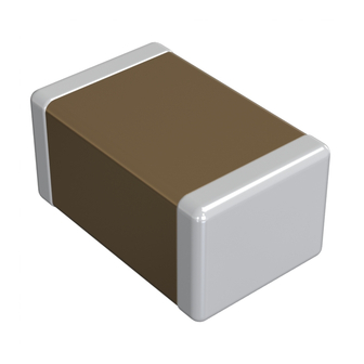
Chip Monolithic Ceramic Capacitor for General
GRM32ER60G227ME05_ (1210, X5R:EIA, 220uF, DC4V)
_: packaging code
1.Scope
This product specification is applied to Chip Monolithic Ceramic Capacitor used for General Electronic equipment.
2.MURATA Part NO. System
(Ex.)
GRM
32
(1)L/W
Dimensions
3. Type & Dimensions
(1)-1 L
(1)-2 W
3.2±0.3
2.5±0.3
4.Rated value
(3) Temperature Characteristics
(Public STD Code):X5R(EIA)
Temp. coeff
or Cap. Change
-15 to 15 %
5.Package
mark
(8) Packaging
f180mm Reel
L
EMBOSSED W8P4
f330mm Reel
K
EMBOSSED W8P4
Product specifications in this catalog are as of Mar.5,2016,and are subject to change or obsolescence without notice.
Please consult the approval sheet before ordering.
Please read rating and !Cautions first.
GRM32ER60G227ME05-01
E
R6
(2)T
(3)Temperature
Characteristics
Dimensions
(2) T
e
2.5±0.3
0.3 min.
(4)
Rated
Temp. Range
Voltage
(Ref.Temp.)
-55 to 85 °C
DC 4 V
(25 °C)
Packaging Unit
1000 pcs./Reel
4000 pcs./Reel
0G
227
(4)Rated
(6)Capacitance
(5)Nominal
Voltage
Tolerance
Capacitance
(Unit:mm)
g
1.0 min.
Specifications and Test
(6)
(5) Nominal
Capacitance
Capacitance
Tolerance
220 uF
±20 %
1
Reference Sheet
M
E05
L
(7)Murata's
(8)Packaging
Control Code
Code
Methods
(Operating
Temp. Range)
-55 to 85 °C
Advertisement

Related Manuals for Murata GRM32ER60G227ME05 Series

Summary of Contents for Murata GRM32ER60G227ME05 Series
- Page 1 Chip Monolithic Ceramic Capacitor for General GRM32ER60G227ME05_ (1210, X5R:EIA, 220uF, DC4V) _: packaging code Reference Sheet 1.Scope This product specification is applied to Chip Monolithic Ceramic Capacitor used for General Electronic equipment. 2.MURATA Part NO. System (Ex.) (7)Murata’s (4)Rated (6)Capacitance (1)L/W (2)T...
- Page 2 ■ Specifications and Test Methods Test Method Item Specification (Ref. Standard:JIS C 5101, IEC60384) Rated Voltage Shown in Rated value. The rated voltage is defined as the maximum voltage which may be applied continuously to the capacitor. When AC voltage is superimposed on DC voltage, V or V whichever is larger, should be maintained within the rated voltage range.
- Page 3 Test Method Item Specification (Ref. Standard:JIS C 5101, IEC60384) 10 Vibration Appearance No defects or abnormalities. Solder the capacitor on the test substrate shown in Fig.3. Capacitance Within the specified initial value. Kind of Vibration : A simple harmonic motion D.F.
- Page 4 Test Method Item Specification (Ref. Standard:JIS C 5101, IEC60384) 16 Durability Appearance No defects or abnormalities. Solder the capacitor on the test substrate shown in Fig.3. Test Temperature : Max. Operating Temp. +/-3℃ Capacitance Within +/-12.5% Test Time : 1000+/-12h Change Applied Voltage : 150% of the rated voltage...
- Page 5 Package GRM Type 1.Tape Carrier Packaging(Packaging Code:D/E/W/F/L/J/K) 1.1 Minimum Quantity(pcs./reel) φ180mm reel φ330mm reel Paper Tape Plastic Tape Paper Tape Plastic Tape Type Code:D/E Code:W Code:L Code:J/ F Code:K GRM01 50000(W4P1) GRM02 40000(W4P1) 15000(W8P2) 50000(W8P2) GRM03 15000(W8P2) 30000(W8P1) 50000(W8P2) 10000(W8P2) 50000(W8P2) 20000(W8P2) 50000(W8P2)
- Page 6 Package GRM Type (2)GRM03/15(W8P2 CODE:D/E/J/F) *1,2:2.0±0.05 (in:mm) 4.0±0.1 +0.1 φ1.5 A A 0.05 max. Dimensions(Chip) Type A *3 B *3 0.2 +0.02/-0.04 0.6±0.03 0.3±0.03 0.37 0.67 0.3±0.03 0.5 max. GRM03 3 0.6±0.05 0.3±0.05 0.3±0.05 0.39 0.69 0.3±0.09 0.6 max. 0.6±0.09 0.3±0.09 0.44 0.74...
- Page 7 Package GRM Type (4)GRM18/21/31/32 (in:mm) <Plastic Tape> <Paper Tape> 4.0±0.1 4.0±0.1 4.0±0.1 4.0±0.1 2.0±0.1 0.25±0.1(T≦2.0mm) +0.1 φ1.5 2.0±0.1 0.3±0.1(T:2.5mm) +0.1 φ1.5 A A Dimensions(Chip) Dimensions Type of Tape 1.6±0.1 0.8±0.1 1.05±0.10 1.85±0.10 0.5 +0/-0.1 0.8 max. 0.5±0.05 1.6±0.2 0.8±0.2 1.10±0.10 2.00±0.10 0.6 +0/-0.1 GRM18...
- Page 8 Package GRM Type (5)GRM43/55 (in:mm) 8.0±0.1 4.0±0.1 0.3±0.1 +0.1 φ1.5 *:2.0±0.1 A +0.2 φ1.5 Dimensions(Chip) Type A *1 B *1 1.15±0.1 1.35±0.15 2.5 max. 1.8±0.2 GRM43 4.5±0.4 3.2±0.3 2.0±0.2 3.7 max. 2.5±0.2 2.8±0.2 4.7 max. 1.15±0.1 1.35±0.15 2.5 max. 1.6±0.2 GRM55 5.7±0.4 5.0±0.4...
- Page 9 め状態 ( 単位: mm) Package GRM Type Fig.1 Package Chips (in:mm) Chip Fig.2 Dimensions of Reel 2.0±0.5 φ21±0.8 w Fig.3 Taping Diagram GRM01/02 8.0 max. 5±1.5 GRM03/15/18/21/31/32 16.5 max. 10±1.5 GRM43/55 20.5 max. 14±1.5 Top Tape : Thickness 0.06 Feeding Hole :As specified in 1.2. Hole for Chip : As specified in 1.2.
- Page 10 Package チップ詰め状態 ( 単位: mm) GRM Type 1.3 Tapes for capacitors are wound clockwise shown in Fig.3. (The sprocket holes are to the right as the tape is pulled toward the user.) 1.4 Part of the leader and part of the vacant section are attached as follows. Tail vacant Section Chip-mounting Unit Leader vacant Section...
-
Page 11: Limitation Of Applications
Caution ■Limitation of Applications Please contact us before using our products for the applications listed below which require especially high reliability for the prevention of defects which might directly cause damage to the third party's life, body or property. ①Aircraft equipment ②Aerospace equipment ③Undersea equipment ④Power plant control equipment... - Page 12 Caution 2.Measurement of Capacitance 1. Measure capacitance with the voltage and frequency specified in the product specifications. 1-1. The output voltage of the measuring equipment may decrease occasionally when capacitance is high. Please confirm whether a prescribed measured voltage is impressed to the capacitor. 1-2.
- Page 13 Caution 5. DC Voltage and AC Voltage Characteristic 1. The capacitance value of a high dielectric constant type [Example of DC Voltage Characteristics] capacitor changes depending on the DC voltage applied. 0.1μF, Rated Voltage 50VDC Sample: X7R(R7) Characteristics Please consider the DC voltage characteristics when a capacitor is selected for use in a DC circuit.
- Page 14 Caution ■Soldering and Mounting 1.Mounting Position 1. Confirm the best mounting position and direction that minimizes the stress imposed on the capacitor during flexing or bending the printed circuit board. 1-1.Choose a mounting position that minimizes the stress imposed on the chip during flexing or bending of the board. ...
- Page 15 Caution 3.Maintenance of the Mounting (pick and place) Machine 1. Make sure that the following excessive forces are not applied to the capacitors. 1-1. In mounting the capacitors on the printed circuit board, any bending force against them shall be kept to a minimum to prevent them from any damage or cracking.
- Page 16 Caution 4-1.Reflow Soldering 1. When sudden heat is applied to the components, the [Standard Conditions for Reflow Soldering] mechanical strength of the components will decrease because a sudden temperature change causes deformation inside the components. In order to prevent Temperature(℃) mechanical damage to the components, preheating is Soldering Peak Temperature...
- Page 17 Caution 4-2.Flow Soldering [Standard Conditions for Flow Soldering] 1. Do not apply flow soldering to chips not listed in Table 2. Table 2 Temperature(℃) Soldering Soldering Temperature Differential Series Chip Dimension(L/W) Code Peak Gradual Temperature ΔT Cooling ΔT≦150℃ 18/21/31 Preheating Peak Temperature 2.
- Page 18 Caution 4-3.Correction of Soldered Portion When sudden heat is applied to the capacitor, distortion caused by the large temperature difference occurs internally, and can be the cause of cracks. Capacitors also tend to be affected by mechanical and thermal stress depending on the board preheating temperature or the soldering fillet shape, and can be the cause of cracks.
- Page 19 Caution 5.Washing Excessive ultrasonic oscillation during cleaning can cause the PCBs to resonate, resulting in cracked chips or broken solder joints. Take note not to vibrate PCBs. 6.Electrical Test on Printed Circuit Board 1. Confirm position of the support pin or specific jig, when inspecting the electrical performance of a capacitor after mounting on the printed circuit board.
- Page 20 Caution (1) Example of a suitable jig [In the case of Single-side Mounting] An outline of the board separation jig is shown as follows. Recommended example: Stress on the component mounting position can be minimized by holding the portion close to the jig, and bend in the direction towards the side where the capacitors are mounted. Not recommended example: The risk of cracks occurring in the capacitors increases due to large stress being applied to the component mounting position, if the portion away from the jig is held and bent in the direction opposite the side where the capacitors are mounted.
- Page 21 Caution (3) Example of Router Type Separator [ Outline Drawing ] Router The router type separator performs cutting by a router rotating at a high speed. Since the board does not bend in the cutting process, stress on the board can be suppressed during board separation.
- Page 22 Caution ■ Others 1. Under Operation of Equipment 1-1. Do not touch a capacitor directly with bare hands during operation in order to avoid the danger of an electric shock. 1-2. Do not allow the terminals of a capacitor to come in contact with any conductive objects (short-circuit). Do not expose a capacitor to a conductive liquid, inducing any acid or alkali solutions.
- Page 23 Notice ■ Rating 1.Operating Temperature 1. The operating temperature limit depends on the capacitor. 1-1. Do not apply temperatures exceeding the maximum operating temperature. It is necessary to select a capacitor with a suitable rated temperature that will cover the operating temperature range. It is also necessary to consider the temperature distribution in equipment and the seasonal temperature variable factor.
- Page 24 Notice ■Soldering and Mounting 1.PCB Design 1. Notice for Pattern Forms 1-1. Unlike leaded components, chip components are susceptible to flexing stresses since they are mounted directly on the substrate. They are also more sensitive to mechanical and thermal stresses than leaded components. Excess solder fillet height can multiply these stresses and cause chip cracking.
- Page 25 Notice 2. Land Dimensions Chip Capacitor 2-1. Chip capacitors can be cracked due to the stress Land of PCB bending , etc. if the land area is larger than needed and has an excess amount of solder. Please refer to the land dimensions in table 1 for flow soldering, table 2 for reflow soldering.
- Page 26 Notice 3. Board Design When designing the board, keep in mind that the amount of strain which occurs will increase depending on the size and material of the board. Relationship with amount of strain to the board thickness, length, width, etc.] ε= Relationship between load and strain 2Ewh...
- Page 27 Notice 5.Flow Soldering [As a Single Chip] Set temperature and time to ensure that leaching of the terminations does not exceed 25% of the chip end area as a single chip (full length of the edge A-B-C-D shown at right) and 25% of the length A-B shown as Termination mounted on substrate.
- Page 28 Notice ■ Others 1.Transportation 1. The performance of a capacitor may be affected by the conditions during transportation. 1-1. The capacitors shall be protected against excessive temperature, humidity and mechanical force during transportation. (1) Climatic condition ・ low air temperature : -40℃ ・...
- Page 29 NOTE 1.Please make sure that your product has been evaluated in view of your specifications with our product being mounted to your product. 2.Your are requested not to use our product deviating from this product specification. 3.We consider it not appropriate to include any terms and conditions with regard to the business transaction in the product specifications, drawings or other technical documents.
Need help?
Do you have a question about the GRM32ER60G227ME05 Series and is the answer not in the manual?
Questions and answers