ST STM32WL Series User Manual
Connectivity expansion board
Hide thumbs
Also See for STM32WL Series:
- Programming manual (262 pages) ,
- Programming manual (262 pages) ,
- Application note (56 pages)
Table of Contents
Advertisement
Quick Links
UM3127
User manual
STM32WL5MOC connectivity expansion board
Introduction
The
B-WL5M-SUBG1
STM32WL connectivity expansion board provides an affordable and flexible way for users to try out new
concepts and build prototypes with the STM32WL series
STM32WL5MOC
microcontroller module.
The B-WL5M-SUBG1 product requires a separate probe for programming and debugging. The STLINK-V3SET debugger can
be connected through a MIPI10/STDC14 cable.
®
The B-WL5M-SUBG1 STM32WL connectivity expansion board is provided with a USB Type-C
connector on an add-on
STMod+ adapter board.
The B-WL5M-SUBG1 product is provided with the STM32WL comprehensive software HAL library and various packaged
software examples available with the
STM32CubeWL
MCU Package.
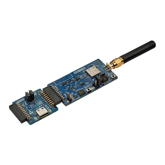
Figure 1.
B-WL5M-SUBG1 product
Picture is not contractual.
UM3127 - Rev 1 - January 2024
www.st.com
For further information contact your local STMicroelectronics sales office.
Advertisement
Table of Contents

Related Manuals for ST STM32WL Series


Summary of Contents for ST STM32WL Series
-
Page 1: Figure 1. B-Wl5M-Subg1 Product
Introduction B-WL5M-SUBG1 STM32WL connectivity expansion board provides an affordable and flexible way for users to try out new concepts and build prototypes with the STM32WL series STM32WL5MOC microcontroller module. The B-WL5M-SUBG1 product requires a separate probe for programming and debugging. The STLINK-V3SET debugger can be connected through a MIPI10/STDC14 cable. -
Page 2: Features
UM3127 Features Features • STM32WL connectivity expansion board embedding an STM32WL5MOC module including: – Ultra‑low‑power STM32WL55JC microcontroller multiprotocol LPWAN dual‑core based on ‑M4/M0+, featuring 256 Kbytes of flash memory and 64 Kbytes of SRAM in a ® ® Cortex UFBGA73 package ®... -
Page 3: Ordering Information
Codification explanation B-XXYY-ZZZZT Description Example: B-WL5M-SUBG1 Expansion board Connectivity expansion board MCU series in STM32 32-bit Arm Cortex MCUs STM32WL series MCU product line in the series STM32WL5M line ® Sub‑gigahertz wireless network based on LoRa , (G)FSK, ZZZZ Wireless network... -
Page 4: Development Environment
UM3127 Development environment Development environment B-WL5M-SUBG1 STM32WL connectivity expansion board runs with the STM32WL5MOC module including ® ® ‑M4/M0+ processor. the STM32WL5MOCH6 32-bit microcontroller based on the Arm Cortex System requirements ® ® ® • Multi‑OS support: Windows 10, Linux 64-bit, or macOS ®... -
Page 5: Conventions
UM3127 Conventions Conventions Table 3 provides the conventions used for the ON and OFF settings in the present document. Table 3. ON/OFF convention Convention Definition Jumper JPx ON Jumper fitted Jumper JPx OFF Jumper not fitted Jumper JPx [1-2] Jumper fitted between Pin 1 and Pin 2 Solder bridge SBx ON SBx connections closed by 0 Ω... -
Page 6: Quick Start
STM32WL5MOC module. Before installing and using the product, accept the evaluation product license agreement from the www.st.com/epla page. For more information on the B-WL5M-SUBG1 STM32WL connectivity expansion board product and demonstration software, visit the www.st.com/stm32nucleo... -
Page 7: Hardware Layout And Configuration
CEB MB1779 board. The mechanical dimensions of the board are shown in Figure Figure 2. MB1779 hardware block diagram (U3) STM32WL5MOC module Temperature sensor (U14) 32 MHz 32 kHz (U14) ST-SAFE I2C bus TCXO Crystal EEPROM Barometer (U8) (U4) (U4) GPIO Accelerometer-... -
Page 8: Mb1779 Mechanical Drawing
UM3127 Hardware layout and configuration Figure 4. MB1779 bottom layout EMS sticker (reserved for EMS) UID64 sticker SMA antenna connector STMod+ (CN2) connector (CN1) Board sticker E5V supply connector (U15) • The UID64 sticker: A 64-bit unique device identification (UID64) is stored in the flash memory and can be accessed by the CPUs, at 0x1FFF7580 base address. -
Page 9: Mb1880 Stmod+ Adapter Board
UM3127 Hardware layout and configuration MB1880 STMod+ adapter board The MB1880 STMod+ adapter board is a very simple board that allows the MB1779 connectivity expansion board to become a host with the add-on STMod+ connectors (female). Figure 6 shows the basic hardware block diagram. Figure 7 Figure 8 show the location of the main... -
Page 10: Mb1880 Mechanical Drawing
UM3127 Hardware layout and configuration Figure 8. MB1880 bottom layout Board sticker EMS sticker (reserved for EMS) STMod+ STMod+ connector connector (CN2) (CN3) Two stickers (the board sticker and an EMS sticker) are present on the bottom side of the MB1880 board: 1. -
Page 11: Power Supply
Figure 10. CEB MB1779 board power tree E5V connector (CN4) SB38 ON Memories: E3V3 connector CMOS serial flash memory (U10) (CN5) C bus EEPROM (U8) ST-SAFE (VDD_RF) SB35 OFF (VDD_SYS) (VBAT) 3V3 LDO SB14 ON JP2 ON (VREF+) (PB0_VDD_TCXO) STDC14... -
Page 12: Power Supply Input E5V Connector (Default Setting)
UM3127 Hardware layout and configuration 6.3.1 Power supply input E5V connector (default setting) The CEB MB1779 board can be powered from the E5V connector (CN4) by either: • Plugging an external 5 V voltage supply (from 3.6 up to 5.5 V) •... -
Page 13: Power Via The Stmod+ Adapter Board (Mb1880) Supplied Through A Usb Type-C
UM3127 Hardware layout and configuration 6.3.2 ® Power via the STMod+ adapter board (MB1880) supplied through a USB Type-C connector ® The CEB MB1779 board can be powered by 5V coming from the USB Type-C connector of the STMod+ adapter ®... -
Page 14: Power Supply Input E3V3 Connector
UM3127 Hardware layout and configuration 6.3.4 Power supply input E3V3 connector The CEB MB1779 board can be powered by the E3V3 connector (CN5) by plugging an external 3.3 V voltage supply (up to 3.6 V). Refer to Table Table 7. External power source E3V3 (3.3 V) Input power name Connector pins... -
Page 15: Board Functions
High-power transmission, and Low-power transmission modes. The choice between the two transmission modes can be done dynamically, thanks to two DC switches controlled by SW_RF (GPIO from the STM32WL series MCU): • The transmission high-output power amplifier (PA HP) is supplied from the PA regulator (REG PA) up to 3.1 V. -
Page 16: Figure 15. Rf Block Diagram
UM3127 Hardware layout and configuration The RF block diagram around the STM32WL5MOC module is displayed in Figure Figure 15. RF block diagram VDD_RF VDDRF VDDSMPS SMPS part VLXSMPS Power management VFBSMPS PB0-VDD_TCXO VDDRF1V55 STM32WL transceiver (STM32WL55JC MCU in BGA92 package) switch VDDPA TCXO... -
Page 17: Figure 17. Schematic Focus On The Rf Part
UM3127 Hardware layout and configuration The two DC switches U1 and U5 are used to realize various output power operation modes. Figure 17. Schematic focus on the RF part SMA connector STM32WL5MOC module DC switches Antenna filter (not needed) Three output power modes are available: 1. -
Page 18: Table 8. Rf Transceiver Configuration
GPIOs The choice between both Tx paths can be done dynamically thanks to the two XS3A1T3157 DC switches (U1 and U5) controlled by SW_CTRL (GPIO from the STM32WL series MCU): • The transmit high output power amplifier (PA HP) is supplied from the PA regulator (REG PA) up to 3.1 V. -
Page 19: Trace Antenna Design
UM3127 Hardware layout and configuration 6.4.4 Trace antenna design To ensure an efficient transmission through the air, it is necessary to have a proper trace antenna design. So, an appropriate antenna type and PCB design must be taken into account. To feed an antenna, transmission lines on PCBs, designed considering their characteristic impedances, are used. -
Page 20: Figure 23. Microstrip Design On A 2-Layer Pcb
UM3127 Hardware layout and configuration Figure 23. Microstrip design on a 2‑layer PCB Figure 24. Coplanar waveguide design on a 2‑layer PCB A 4‑layer PCB can also be used as soon as the RF trace remains controlled to 50 Ω. Some general guidelines when routing an RF PCB are listed below: •... -
Page 21: Stsafe
Hardware layout and configuration Below is displayed the RF track routing of the B-WL5M-SUBG1 product. Antenna connector recommendations The SMA-J-P-H-ST-EM1 SMA connector from SAMTEC can be used. This kind of SMA connector is standard so an equivalent SMA connector can be used. 6.4.5 STSAFE Two variants of the STM32WL5MOC module are available. -
Page 22: Current Consumption Measurement (Idd)
UM3127 Hardware layout and configuration 6.4.6 Current consumption measurement (IDD) The IDD-labeled jumper (JP2) is used to measure the STM32WL5MOC module power consumption by removing the jumper and connecting an ammeter. Its location in the power structure is shown in Figure 1. -
Page 23: Solder Bridges
UM3127 Hardware layout and configuration Solder bridges There are 38 solder bridges on the MB1779 board, and there is one solder bridge on the MB1880 board. Table 10. Solder bridge configuration on MB1779 Solder bridge (SB) Function State Description STMOD+_UA UART1_RTS connected to pin 1 of the STMod+ connector RT1_RTS (SB1 and SB3 are exclusive) - Page 24 UM3127 Hardware layout and configuration Solder bridge (SB) Function State Description 3V3_MEMs is connected to 3V3 SB15 3V3_MEMs VDD_APP is not connected to 3V3 (MEMS U2, U4, U7, and U14 is not supplied. UART1_TX is connected to pin 3 of the STMod+ connector SB16 STMOD+_UA RT1_TX...
-
Page 25: Table 11. Solder Bridge Configuration On Mb1880
UM3127 Hardware layout and configuration Solder bridge (SB) Function State Description STMOD+_I2C I2C2_SDA connected to pin 10 of the STMod+ connector 2_SDA SB31 I2C2_SDA not connected to pin 10 of the STMod+ connector (PA11) ALERT/INT pin TEMP_INT signal from the STM32WL5MOC module connected of U14 to the ALERT/INT pin of U14. -
Page 26: Jumpers
UM3127 Hardware layout and configuration Jumpers 6.6.1 MB1779 jumper The jumper JP1 labeled IDD, is used to measure the STM32WL5MOC module power consumption by removing the jumper and by connecting an ammeter. Refer to Section 6.4.6. 6.6.2 MB1880 jumpers The MB1880 board has two parallel jumpers as shown in Figure Figure 8, and... -
Page 27: Embedded Devices
UM3127 Hardware layout and configuration Embedded devices Embedded sensors and the EEPROM are connected to the STM32WL5MOC module with an I C bus. The address is a 7‑bit address with an additional read/write bit (HIGH for reading, LOW for writing). Table 13 describes the different addresses to read or write action for each component:... -
Page 28: Barometer (U4)
UM3127 Hardware layout and configuration Figure 28. 3D accelerometer and 3D gyroscope (U2) pin 1 location 6.7.3 Barometer (U4) U4 is connected to the STM32WL5MOC module through the I C interface. U4 is an ultracompact piezoresistive absolute pressure sensor that functions as a digital output barometer. 6.7.4 Magnetometer (U7) U7 is connected to the STM32WL5MOC module through the I... -
Page 29: Board Connectors
UM3127 Board connectors Board connectors Several connectors are implemented on the B-WL5M-SUBG1 product: • Five connectors are implemented on the MB1779 expansion board. • Three connectors are implemented on the MB1880 fan-out board. MB1779 STMod+ (CN1) CN1 is an STMod+ connector (male). This connector allows interfacing the MB1779 board to: •... - Page 30 UM3127 Board connectors Pin number STM32 pin Function PB14 INTERRUPT CM4_EVENTOUT (if SB11 ON) NRST NRST (if SB10 ON) ADC (ADC1_IN6) TIM2CH3 5 V supply GPIO PB10 GPIO GPIO PC13 GPIO 1. The default configuration is in bold UM3127 - Rev 1 page 30/47...
-
Page 31: Mb1779 Debugging Connector (Cn3)
UM3127 Board connectors MB1779 debugging connector (CN3) This connector is a 2x7‑pin 1.27 mm pitch male connector. It allows the connection to an STLINK-V3SET using ® ® the SWD protocol, respecting the MIPI10/ARM10 pinout (Arm Cortex debug connector). The related pinout for the STDC14 connector is listed in Table Figure 32. -
Page 32: Stlink-V3E Debugger
UM3127 Board connectors 7.2.1 STLINK-V3E debugger As there is no embedded STLINK-V3E on the CEB MB1779, the only way to program and debug the onboard STM32WL5MOC module is by using an external debug tool connected to the STDC14 connector (CN3). The external debugger recommended is STLINK-V3SET, which supports SWD and VCP for STM32 devices. -
Page 33: Mb1779 2-Pin E3V3 Connector (Cn5)
UM3127 Board connectors MB1779 2‑pin E3V3 connector (CN5) The CN5 is a standard 2‑pin E3V3 connector (2.54 mm pitch), not mounted on the CEB board. The CEB MB1779 board can be powered from the E3V3 connector (CN5) by plugging an external 3.3 V voltage supply (up to 3.6 V). Figure 35. -
Page 34: Mb1880 Stmod+ Connectors (Cn2 And Cn3)
UM3127 Board connectors MB1880 STMod+ connectors (CN2 and CN3) The MB1880 STMod+ adapter board transforms the MB1779 CEB board from an expansion board to a host board. Table 18. STMod+ pin assignment and description CN2 pins CN3 pins Pin name Pin name number number... -
Page 35: Stm32Wl5Moc I/O Assignment
UM3127 STM32WL5MOC I/O assignment STM32WL5MOC I/O assignment Table 19. STM32WL5MOC I/O assignment Pin name Signal Feature NRST T_NRST STM32WL5MOC reset STMOD+_UART1_RX UART1_RX on pin 2 of the STMod+ connector MEMORY_SPI_CS SPI chip select of the CMOS serial flash memory STMOD+_UART1_TX UART1_TX on pin 3 of the STMod+ connector MAGNETO_INT INT pin of magnetometer... - Page 36 UM3127 STM32WL5MOC I/O assignment Pin name Signal Feature PA12 I2C2_SCL I2C2_SCL SPI2_MISO SPI2_MISO User LED2 GPIO PB15 User LED1 GPIO PA14 T_SWCLK T_SWCLK Power supply for RTC, TAMP, external clock 32 kHz VBAT VBAT oscillator, and backup registers (through the power switch) when VDD is not present VREFP VREF+...
-
Page 37: Wl5M-Subg1 Product Information
B01. The second line shows the board serial number used for traceability. Parts marked as “ES” or “E” are not yet qualified and therefore not approved for use in production. ST is not responsible for any consequences resulting from such use. In no event will ST be liable for the customer using any of these engineering samples in production. -
Page 38: Board Revision History
UM3127 B-WL5M-SUBG1 product information Board revision history Table 21. Board revision history Board reference Board variant and revision Board change description Board limitations MB1779 HIGH‑BAND‑B02 Initial revision No limitation (expansion board) MB1880 uart-A01 Initial revision No limitation (STMod+ adapter board) UM3127 - Rev 1 page 38/47... -
Page 39: Federal Communications Commission (Fcc) And Ised Canada Compliance
UM3127 Federal Communications Commission (FCC) and ISED Canada Compliance Statements Federal Communications Commission (FCC) and ISED Canada Compliance Statements Applicable for products with order code B-WL5M-SUBG1. 10.1 FCC Compliance Statement FCC Compliance Statement The MB1779‑HIGH‑BAND‑B02 contains a module from STMicroelectronics, Model: STM32WL5MOC •... -
Page 40: Ised Compliance Statement
UM3127 Federal Communications Commission (FCC) and ISED Canada Compliance Statements 10.2 ISED Compliance Statement This device complies with FCC and ISED Canada RF radiation exposure limits set forth for general population for mobile application (uncontrolled exposure). This device must not be collocated or operating in conjunction with any other antenna or transmitter. -
Page 41: Red Compliance Statement
STMicroelectronics déclare que l'équipement radioélectrique du type "B-WL5M-SUBG1" est conforme à la directive 2014/53/UE. Le texte complet de la déclaration UE de conformité est disponible à l'adresse internet suivante: www.st.com. Bande de fréquence utilisée en transmission et puissance maximale rayonnée dans cette bande : •... -
Page 42: Revision History
UM3127 Revision history Table 22. Document revision history Date Revision Changes 11-Jan-2024 Initial release. UM3127 - Rev 1 page 42/47... -
Page 43: Table Of Contents
UM3127 Contents Contents Features................2 Ordering information . - Page 44 UM3127 Contents 6.7.2 3D accelerometer and 3D gyroscope (U2) ........27 6.7.3 Barometer (U4) .
-
Page 45: List Of Tables
UM3127 List of tables List of tables Table 1. List of available products............. . . 3 Table 2. -
Page 46: List Of Figures
UM3127 List of figures List of figures Figure 1. B-WL5M-SUBG1 product ............. 1 Figure 2. - Page 47 ST’s terms and conditions of sale in place at the time of order acknowledgment. Purchasers are solely responsible for the choice, selection, and use of ST products and ST assumes no liability for application assistance or the design of purchasers’...
Need help?
Do you have a question about the STM32WL Series and is the answer not in the manual?
Questions and answers