Table of Contents
Advertisement
Quick Links
SERVICE MANUAL
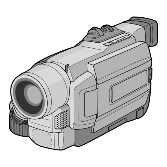
GR-DVL355EG/EK, DVL357EG/EK,
DVL555EG/EK, DVL557EG/EK
SPECIFICATIONS
For General
Power supply
: DC 11.0 V } (Using AC Adapter)
DC 7.2 V } (Using battery pack)
Power consumption
LCD monitor off, viewfinder on
: Approx. 4.3 W
LCD monitor on, viewfinder off
: Approx. 5.3 W
Video light
: Approx. 3.5 W
Dimensions (W x H x D)
: 83 mm x 97 mm x 188 mm
(with the LCD monitor closed and the viewfinder
pushed down)
Weight
: Approx. 610 g
(GR-DVL557/DVL555/DVL450)
Approx. 590 g
(GR-DVL357/DVL355/DVL157/DVL150)
Operating temperature
: 0°C to 40°C
Operating humidity
: 35% to 80%
Storage temperature
: –20°C to 50°C
Pickup
: 1/4" CCD
Lens
: F 1.8, f = 3.6 mm to 36 mm, 10:1 power zoom lens
Filter diameter
: ø37 mm
LCD monitor
: 3.5" diagonally measured, LCD panel/TFT active matrix system
(GR-DVL557/DVL555/DVL450)
2.5" diagonally measured, LCD panel/TFT active matrix system
(GR-DVL357/DVL355/DVL157/DVL150)
Viewfinder
: Electronic viewfinder with 0.44" colour LCD
(GR-DVL557/DVL555/DVL450)
Electronic viewfinder with 0.24" black/white LCD
(GR-DVL357/DVL355/DVL157/DVL150)
Speaker
: Monaural
For Digital Video Camera
Format
: DV format (SD mode)
Signal format
: PAL standard
Recording/Playback format
: Video: Digital component recording
: Audio: PCM digital recording, 32 kHz 4-channel (12-bit),
48 kHz 2-channel (16-bit)
Cassette
: Mini DV cassette
Tape speed
: SP: 18.8 mm/s
LP: 12.5 mm/s
Maximum recording time
: SP: 80 min.
(using 80 min. cassette)
LP: 120 min.
DIGITAL VIDEO CAMERA
(The specifications shown pertain specifically to the model GR-DVL150/157/355/357/450/555/557)
Camcorder
This service manual is printed on 100% recycled paper.
COPYRIGHT © 2001 VICTOR COMPANY OF JAPAN, LTD.
For Digital Still Camera (GR-DVL557/DVL555/DVL357/DVL355 only)
Storage media
: SD Memory Card/MultiMediaCard
Compression system
: JPEG (compatible)
File size
: VGA (640 x 480 pixels)
Picture quality
: 2 modes (FINE/STANDARD)
Approximate number of storable images
with memory card [8 MB] (provided)
FINE
: 100
STANDARD
: 200
with memory card [16 MB] (optional)
FINE
: 200
STANDARD
: 400
with memory card [32 MB] (optional)
FINE
: 400
STANDARD
: 800
with memory card [64 MB] (optional)
FINE
: 800
STANDARD
: 1600
For Connectors
S-Video
: Y : 1 V (p-p), 75 Ø, analogue
Output
C : 0.29 V (p-p), 75 Ø, analogue
: Y : 0.8 V (p-p) – 1.2 V (p-p), 75 Ø, analogue
Input (GR-DVL557 only)
C : 0.2 V (p-p) – 0.4 V (p-p), 75 Ø, analogue
AV
: 1 V (p-p), 75 Ø, analogue
Video output
: 0.8 V (p-p) – 1.2 V (p-p), 75 Ø, analogue
Video input (GR-DVL557 only)
Audio output
: 300 mV (rms), 1 kØ, analogue, stereo
Audio input (GR-DVL557 only)
: 300 mV (rms), 50 kØ, analogue, stereo
DV
Output
Input (GR-DVL557/DVL357/DVL157 only)
USB (GR-DVL557/DVL555/DVL357/DVL355 only)
PC (DIGITAL PHOTO)
(GR-DVL450/DVL157/DVL150 only)
EDIT (GR-DVL557/DVL555/DVL357/DVL355 only)
JLIP (GR-DVL450/DVL157/DVL150 only)
AC adapter AP-V10EG
Power requirement
: AC 110 V to 240 V`, 50 Hz/60 Hz
Output
: DC 11 V } , 1 A
Dimensions (W x H x D)
: 59 mm x 31 mm x 84 mm
Weight
: Approx. 140 g (not including Power Cord)
Specifications shown are for SP mode unless otherwise indicated. E & O.E. Design and specifications
subject to change without notice.
: 4-pin, IEEE 1394 compliant
: 4-pin, IEEE 1394 compliant
: 5-pin
: ø2.5 mm, 3-pole
: ø3.5 mm, 2-pole
: ø3.5 mm, 4-pole
No. 86614
February 2001
Advertisement
Table of Contents

Related Manuals for JVC GR-DVL355EG


Summary of Contents for JVC GR-DVL355EG
- Page 1 SERVICE MANUAL DIGITAL VIDEO CAMERA GR-DVL355EG/EK, DVL357EG/EK, DVL555EG/EK, DVL557EG/EK SPECIFICATIONS (The specifications shown pertain specifically to the model GR-DVL150/157/355/357/450/555/557) For Digital Still Camera (GR-DVL557/DVL555/DVL357/DVL355 only) Camcorder Storage media : SD Memory Card/MultiMediaCard Compression system : JPEG (compatible) For General File size...
-
Page 2: Table Of Contents
2.8 JIG CONNECTOR CABLE CONNECTION ......2-20 3. ELECTRICAL ADJUSTMENT 3.1 PRECAUTION ..............3-1 3.2 SETUP .................. 3-2 The following table lists the differing points between Models GR-DVL355EG/EK,GR-DVL357EG/EK,GR-DVL555EG/EK and GR-DVL557EG/EK in this series. GR-DVL355EG GR-DVL355EK GR-DVL357EG GR-DVL357EK GR-DVL555EG GR-DVL555EK GR-DVL557EG GR-DVL557EK... -
Page 3: Important Safety Precautions
Important Safety Precautions Prior to shipment from the factory, JVC products are strictly inspected to conform with the recognized product safety and electrical codes of the countries in which they are to be sold. However, in order to maintain such compliance, it is equally important to implement the following precautions when a set is being serviced. - Page 4 • Safety Check after Servicing Examine the area surrounding the repaired location for damage or deterioration. Observe that screws, parts and wires have been returned to original positions, Afterwards, perform the following tests and confirm the specified values in order to verify compliance with safety standards.
-
Page 6: Disassembly
SECTION 1 DISASSEMBLY 1.1 BEFORE ASSEMBLY AND DISASSEMBLY 1.1.4 Disconnection of Connectors (Wires) 1.1.1 Precautions Connector Pull both ends of the connector in the arrow direction, re- 1. Be sure to remove the power supply unit prior to mount- move the lock and disconnect the flat wire. ing and soldering of parts. -
Page 7: Jigs And Tools Required For Disassembly, Assembly And Adjustment
1.2 JIGS AND TOOLS REQUIRED FOR DISASSEMBLY, 1.3 DISASSEMBLY/ASSEMBLY OF CABINET PARTS ASSEMBLY AND ADJUSTMENT AND BOARD ASSEMBLY 1.2.1 Tools required for adjustments 1.3.1 Disassembly flow chart This flowchart indicates the disassembly step for the cabi- Torque Driver YTU94088 YTU94088-003 net parts and board assembly in order to gain access to item(s) to be serviced. -
Page 8: Disassembly Method
1.3.2 Disassembly method NOTE Remove the CAP (DC JACK) before removing STEP Fig.No. PART POINT NOTE these parts . a: As it is difficult to remove (L 3 b), remove the COVER(ZOOM) Fig.1-3-1 (S1a),(S1b),2(L1a),2(L1b ) NOTE ASSY F. COVER ASSY by lowering it. UPPER CASE ASSY Fig.1-3-2 (S2a),(S2b),(L2),(S2c) NOTE2 NOTE... - Page 9 (DC JACK) NOTE (BOTTOM SIDE) (REAR SIDE) Fig. 1-3-2 COVER (JACK) NOTE NOTE Fig. 1-3-3...
- Page 10 BRACKET (OP) ASSY Fig. 1-3-4 NOTE Fig. 1-3-5...
- Page 11 NOTE Fig. 1-3-6 SHIELD PLATE NOTE EJECT SW NOTE Fig. 1-3-7 Fig. 1-3-8...
- Page 12 NOTE PLATE (SPK) NOTE Fig. 1-3-9 NOTE NOTE NOTE NOTE NOTE COVER (HINGE) : 0.147N·m (1.5kgf·cm) Fig. 1-3-10...
-
Page 13: Monitor Assembly
MONITOR ASSEMBLY 3. Unplug the wires and FPCs from the two connectors b , c , and then remove the MONITOR BL board assembly, Note: The shape of the monitor assembly varies by the size holder (PWB) and backlight in that order. of the LCD screen. -
Page 14: Disassembly/Assembly Of Monitor Assembly (For 3.5"-Type Lcd)
Note: The shape of the monitor assembly varies depend- 3. Unplug the wires and FPCs from the two connectors b , ing on the size of the LCD screen. c , and then remove the MONITOR BL board assembly, holder (PWB) and backlight in that order. For the 3.5”-type LCD, refer to Fig. -
Page 15: E. Vf Assembly
E. VF ASSEMBLY Note: The shape of the E. VF assembly varies by the type of the viewfinder (B/W, color VF). For the B/W VF, refer to Fig. 1-5-1. For the COLOR VF, refer to Fig. 1-5-2. 1.5.1 Disassembly/assembly of E. VF assembly (for B/W VF) a: When removing the top case sub-assembly, peel 1. -
Page 16: Disassembly/Assembly Of E. Vf Assembly (For Color Vf)
1.5.2 Disassembly/assembly of E. VF assembly (for Color VF) d: When reassembling the top case sub-assembly, Note: Place the E. VF assembly with the VF case (upper) Note assembly down through the disassembly/assembly be careful not to catch the FPC between any of the parts. -
Page 17: Disassembly/Assembly Of Op Block Assembly/Ccd Board Assembly
1.6 DISASSEMBLY/ASSEMBLY OF OP BLOCK 1.6.3 How to assemble CCD base assembly and CCD ASSEMBLY/CCD BOARD ASSEMBLY board assembly 1. Install the optical LPF with the spacer rubber attached 1.6.1 Precautions to its CCD side in the OP block assembly. 1. -
Page 18: Emergency Display
1.7 EMERGENCY DISPLAY Whenever some abnormal signal is input to the syscon CPU, Example (in case of the error number E01): an error number (E01, as an example) is displayed on the LCD monitor or (in the electronic view finder). In every error status, such the message as shown below alternately appear over and over. -
Page 19: Service Note
1.8 SERVICE NOTE 1-14... -
Page 20: Mechanism Adjustment
SECTION 2 MECHANISM ADJUSTMENT 2.1 PRELIMINARY REMARKS ON ADJUSTMENT AND (3) The symbol (T or B)appearing in this column shows the REPAIR side which the objective part is mounted on. T =the upper side, B =the lower side 2.1.1 Precautions (4) Symbols appearing in this column indicate drawing 1. -
Page 21: Jigs And Tools Required For Disassembly, Assembly And Adjustment
2.2 JIGS AND TOOLS REQUIRED FOR DISASSEMBLY, ASSEMBLY AND ADJUSTMENT 2.2.1 Tools required for adjustments 1. Torque Driver Torque Driver YTU94088 YTU94088-003 Be sure to use to fastening the mechanism and exterior parts because those parts must strictly be controlled for tightening torque. -
Page 22: Disassembly/Assembly Of Mechanism Assembly
2.3 DISASSEMBLY/ASSEMBLY OF MECHANISM <SUB CAM GEAR> ASSEMBLY 2.3.1 General statement The mechanism should generally be disassembled/assem- bled in the EJECT mode (ASSEMBLY mode). (Refer to Fig. 2-3-1.) TOP VIEW BOTTOM VIEW However, when the mechanism is removed from the main body, it is set in the STOP mode. -
Page 23: Mechanism Timing Chart
2.3.3 Mechanism timing chart MODE EJECT C IN SHORT FF STOP PLAY PARTS MAIN CAM (ø10.4) 31.7 45.6 49.5 74.04 129.5 156.6 169.2 211.5 280.3 SUB CAM (ø11) 43.1 46.8 122.5 148.1 ENCODER (ø10) 47.4 51.5 134.7 162.9 291.5 ROTARY ENCODER CAM SW SLIDE END... -
Page 24: Disassembly/Assembly Of Mechanism Assembly
2.4 DISASSEMBLY/ASSEMBLY OF MECHANISM ASSEMBLY 2.4.1 Follow chart 1. Configuration Mechanism assembly Cassette housing assembly Slide deck assembly Main deck assembly Fig. 2-4-1 2. Procedures for disassembly Mechanism assembly Cassette housing assembly Slide deck assembly Main deck assembly Fig. 2-4-2... - Page 25 3. Disassembling procedure table PART NAME FIG. POINT NOTE REMARKS A Cassette housing assembly Fig. 2-4-5 3(S1),(L1a)-(L1d) 1a, 1b, 1c, 1d Adjustment Reel disk (SUP) assembly Fig. 2-4-6 (W2) 2a, 2b Reel disk (TU) assembly Fig. 2-4-6 (W2) 2a, 2b Reel cover assembly Fig.
- Page 26 < TOP VIEW > 4b 11b 11a Main deck assembly Slide deck assembly 7b 7a 7d 7e 9c 3c 3b 7h 2b Fig. 2-4-3 < BOTTOM VIEW > Main deck assembly Slide deck assembly Fig. 2-4-4...
-
Page 27: Disassembly/Assembly
2.4.2 Disassembly/assembly Note 1a: <STOP mode> Shift the mechanism mode 1. A Cassette housing assembly from the STOP mode to the EJECT mode. Cassette Note 1b: housing Reassemble the cassette (L1b) assembly housing assembly to the (S1) mechanism as the cancel lever is moved in the direc- tion of the arrow. - Page 28 3. 3a Tension arm assembly/ 3b Release guide assembly 3b Idler arm assembly/ 3d Guide arm assembly 3c Pinch roller arm assembly Note 3a: When removing the reel cover assembly, pay heed to re- lease guide assembly and guide arm assembly. For, the (W3a) guide arm assembly is just inserted into the slide deck as- sembly from the upside and it is apt to come off after the...
- Page 29 5. 5a Guide roller (SUPPLY) assembly/ 5b Rail assembly Note 5a: When reassembling, insert the tip Guide roller of the guide roller with the coil (s) assembly spring put on it into the hole on the main deck. Tighten the guide roller by about 6 turns so that the Note 5a (P5)
- Page 30 Note 7a: 7. 7a Loading brake assembly/ 7b Guide pin (S) Don’t remove these parts unreasonably. If they are removed 7c Pad arm assembly/ 7d Slide guide plate assembly for some reason, be very careful not to lose them. 7e Collar/ 7f Collar/ 7g Sub brake assembly 7h Control plate assembly Note 7b: When reinstalling the sub brake assembly, set the control...
- Page 31 9. 9a Loading guide/ 9b Timing belt 9c Center gear assembly/ 9d Motor bracket assembly 9e Worm wheel/ 9f Gear holder Note 9a: Note 9b Note 9a Carefully handle the DEW sensor. (Don’t touch the sensor surface in particular.) Note 9b: When engaging the timing belt, make sure that it securely (S9) engages with the gears of both the center gear assembly and...
- Page 32 11. 11a Catcher (T) assembly/ 11b Capstan motor 11c Charge arm assembly/ 11d Sub cam gear 11e PWB holder Note 11: The following figure shows how to put the charge arm as- sembly and sub cam gear assembly together. (S11) (S11) Note 11 (W11)
-
Page 33: List Of Procedures For Disassembly
2.4.3 List of procedures for disassembly Cassette housing assembly (P5) (L1b) (S9) (W5a) (S9) (W5b) (W5a) (W3b) (S1) (W5a) (W10b) (L1d) (L1a) (S4) (S4) (S4) (S1) (L1c) (S1) (S11) (W10a) (S10) (S11) (S10) (W10a) (S11) (S9) (S11) (W9) (W4) (P4b) (P4a) (S9) (W7) -
Page 34: Checkup And Adjustment Of Mechanism Phase
2.5 CHECKUP AND ADJUSTMENT OF MECHANISM PHASE <Connect gear> (Note 2) Set the connect gear so <Rotary encoder> that its locating hole meets Set the “I” of the rotary the hole on the main deck part at the tapped hole assembly. -
Page 35: Mechanism Adjustments
2.6 MECHANISM ADJUSTMENTS 2.6.1 Assembling slide deck assembly and main deck assembly œ Œ Fig. 2-6-1 Assembling procedure 1. Loosen the screw A. 2. Set the mechanism in the PLAY mode. (Refer to “2.3.2 Explanation of mechanism mode”.) 3. Press the end face B of the slide deck assembly (reel disk side) and the end face C of the main deck assem- bly (drum assembly side) with uniform force so that the two assemblies are tightly pressed to each other. -
Page 36: Locating Tension Pole
2.6.2 Locating tension pole <PLAY mode> Fig. 2-6-2 Locating procedure 1. Enter the mechanism assembly into the PLAY mode. (Refer to “2.3.2 Explanation of mechanism mode”.) 2. When the “ ” part is positioned down, make sure that the part “a” of the tension arm assembly is located within the range of “b”. -
Page 37: Service Note
2.7 SERVICE NOTE Use the following chart to manage mechanism parts that are removed for disassembling the mechanism. A Cassette housing assembly S1×3 Reel disk (SUP) assembly Reel cover assembly W2×1 Reel disk (TU) assembly W2×1 S2b×1 S2a×2 W2×1 Guide arm Tension arm Pinch roller arm Release guide... - Page 38 B Slide deck assembly Loading Slide guide Guide pin Pad arm brake plate (SUPPLY) assembly assembly assembly W7×1 P7a×1 W7×1 S7a×1 W7×1 P7b×1 S7b×1 Control Collar Collar Sub brake plate assembly assembly W7×1 P7c×1 W7×2 P7d×1 W6×1 C Main deck assembly Slide lever Tension lever Brake control...
-
Page 39: Jig Connector Cable Connection
2.8 JIG CONNECTOR CABLE CONNECTION Remove one screw (1) first and the cover (JIG) next. Jig connector cable (YTU93082G) CN105 Cover(JIG) JIG BOARD Fig. 2-8-1 Jig connector cable connection MAIN JIG BOARD CN105 (PIN NO.) (LABEL) AL_3VSYS AL_3VSYS DJIG_SCK 10 DJIG_SPT DJIG_SPT MON_G... -
Page 40: Electrical Adjustment
SECTION 3 ELECTRICAL ADJUSTMENT 3.1 PRECAUTION 3. Tools required for adjustments 1. Precaution Torque Driver Both the camera and deck sections of this model needs a YTU94088 YTU94088-003 personal computer for adjustment except simple adjustment with potentiometers. If some of the following parts is replaced for repair or other reason, the repaired set must be adjusted with a personal computer. -
Page 41: Setup
Torque driver Alignment tape Be sure to use to fastening the mechanism and exte- To be used for check and adjustment of interchange- rior parts because those parts must strictly be control- ability of the mechanism. led for tightening torque. 10. - Page 42 POLY BAG LY32095-005A PACKING CASE,E,F,G,H LY32095-009A PACKING CASE,A,B,C,D LY32096-001A CUSHION QPA02003006 POLY BAG,A,C,E,G YQM30061-3 POLY BAG,B,D,F,H LYT0727-002B INST.BOOK(GE),A,C,E,G MODEL MARK LYT0727-003B INST.BOOK(FR),A,C,E,G GR-DVL355EG LYT0727-004A INST.BOOK(DU),A,C,E,G GR-DVL355EK LYT0727-005B INST.BOOK(SP),A,C,E,G GR-DVL357EG LYT0727-006A INST.BOOK(IT),A,C,E,G GR-DVL357EK LYT0727-007A INST.BOOK(DA),A,C,E,G GR-DVL555EG LYT0727-008A INST.BOOK(FI),A,C,E,G GR-DVL555EK LYT0727-009A INST.BOOK(SW),A,C,E,G LYT0727-010A INST.BOOK(NO),A,C,E,G...
- Page 43 FINAL ASSEMBLY <M2> 101A 104A 101C 101B 102B 102C JUNCTION RATING <05> LABEL 102A MECHANISM ELECTRONIC <M3> VIEWFINDER 251C <M4> 251D 251D JACK <06> 251G 251H 251G 251C 115E 196A 251C 251J 115A 251F 130E 251B 251E <04> 251C 196A 115B MAIN 130E...
- Page 44 REF No. PART No. PART NAME, DESCRIPTION REF No. PART No. PART NAME, DESCRIPTION - - - - - - - - - - - - - - - - - - - - - - - - - - - - - - - - - - - - - - - - - - - - - - - - - - - - - - - - - - - - - - - - - - - - - - - - - - - - - - - - - - - - - - - - - - - - - - - - - - - - - - - - - - - - - - - - - - - - - - - - - - - - - - - - - - - -...
- Page 45 MECHANISM ASSEMBLY <M3> NOTE:The section marked in AA and BB indicate Classification Part No. Symbol in drawing lubrication and greasing areas. Grease KYODO-SH-P YTU94027...
- Page 46 REF No. PART No. PART NAME, DESCRIPTION REF No. PART No. PART NAME, DESCRIPTION - - - - - - - - - - - - - - - - - - - - - - - - - - - - - - - - - - - - - - - - - - - - - - - - - - - - - - - - - - - - - - - - - - - - - - - - - - - - - - - - - - - - - - - - - - - - - - - - - - - - - - - - - - - - - - - - - - - - - - - - - - - - - - - - - - - -...
- Page 47 ELECTRONIC VIEWFINDER ASSEMBLY <M4> [GR-DVL555EG/EK, 557EG] 309 309 REF No. PART No. PART NAME, DESCRIPTION REF No. PART No. PART NAME, DESCRIPTION - - - - - - - - - - - - - - - - - - - - - - - - - - - - - - - - - - - - - - - - - - - - - - - - - - - - - - - - - - - - - - - - - - - - - - - - - - - - - - - - - - - - - - - - - - - - - - - - - - - - - - - - - - - - - - - - - - - - - - - - - - - - - - - - - -...
- Page 48 ELECTRONIC VIEWFINDER ASSEMBLY <M4> [GR-DVL355EG/EK, 357EG/EK, 557EK] 309 309 REF No. PART No. PART NAME, DESCRIPTION REF No. PART No. PART NAME, DESCRIPTION - - - - - - - - - - - - - - - - - - - - - - - - - - - - - - - - - - - - - -...
- Page 49 MONITOR ASSEMBLY <M5> [GR-DVL355EG/EK, 357EG/EK] 501H 501A 501C 501G 501F 501B 501D 501D LCD BL <03> REF No. PART No. PART NAME, DESCRIPTION REF No. PART No. PART NAME, DESCRIPTION - - - - - - - - - - - - - - -...
- Page 50 MONITOR ASSEMBLY <M5> [GR-DVL555EG/EK, 557EG/EK] 501H 501K 501A 501C 501G 501J 501F 501B 501D 501D LCD BL <03> 502A REF No. PART No. PART NAME, DESCRIPTION REF No. PART No. PART NAME, DESCRIPTION - - - - - - - - - - - - - - - - - - - - - - - - - - - - - - - - - - - - - - - - - - - - - - - - - - - - - - - - - - - - - - - - - - - - - - - - - - - - - - - - - - - - - - - - - - - - - - - - - - - - - - - - - - -...
- Page 51 MODEL MARK MODEL MARK GR-DVL355EG GR-DVL555EG GR-DVL355EK GR-DVL555EK ELECTRICAL PARTS LIST GR-DVL357EG GR-DVL557EG GR-DVL357EK GR-DVL557EK REF No. PART No. PART NAME, DESCRIPTION REF No. PART No. PART NAME, DESCRIPTION - - - - - - - - - - - - - - - -...
- Page 52 REF No. PART No. PART NAME, DESCRIPTION REF No. PART No. PART NAME, DESCRIPTION - - - - - - - - - - - - - - - - - - - - - - - - - - - - - - - - - - - - - - - - - - - - - - - - - - - - - - - - - - - - - - - - - - - - - - - - - - - - - - - - - - - - - - - - - - - - - - - - - - - - - - - - - - - - - - - - - - - - - - - - - - - - - - - - - - - -...
- Page 53 REF No. PART No. PART NAME, DESCRIPTION REF No. PART No. PART NAME, DESCRIPTION - - - - - - - - - - - - - - - - - - - - - - - - - - - - - - - - - - - - - - - - - - - - - - - - - - - - - - - - - - - - - - - - - - - - - - - - - - - - - - - - - - - - - - - - - - - - - - - - - - - - - - - - - - - - - - - - - - - - - - - - - - - - - - - - - - - -...
- Page 54 REF No. PART No. PART NAME, DESCRIPTION REF No. PART No. PART NAME, DESCRIPTION - - - - - - - - - - - - - - - - - - - - - - - - - - - - - - - - - - - - - - - - - - - - - - - - - - - - - - - - - - - - - - - - - - - - - - - - - - - - - - - - - - - - - - - - - - - - - - - - - - - - - - - - - - - - - - - - - - - - - - - - - - - - - - - - - - - -...
- Page 55 REF No. PART No. PART NAME, DESCRIPTION REF No. PART No. PART NAME, DESCRIPTION - - - - - - - - - - - - - - - - - - - - - - - - - - - - - - - - - - - - - - - - - - - - - - - - - - - - - - - - - - - - - - - - - - - - - - - - - - - - - - - - - - - - - - - - - - - - - - - - - - - - - - - - - - - - - - - - - - - - - - - - - - - - - - - - - - - -...
- Page 56 REF No. PART No. PART NAME, DESCRIPTION REF No. PART No. PART NAME, DESCRIPTION - - - - - - - - - - - - - - - - - - - - - - - - - - - - - - - - - - - - - - - - - - - - - - - - - - - - - - - - - - - - - - - - - - - - - - - - - - - - - - - - - - - - - - - - - - - - - - - - - - - - - - - - - - - - - - - - - - - - - - - - - - - - - - - - - - - -...
- Page 57 REF No. PART No. PART NAME, DESCRIPTION REF No. PART No. PART NAME, DESCRIPTION - - - - - - - - - - - - - - - - - - - - - - - - - - - - - - - - - - - - - - - - - - - - - - - - - - - - - - - - - - - - - - - - - - - - - - - - - - - - - - - - - - - - - - - - - - - - - - - - - - - - - - - - - - - - - - - - - - - - - - - - - - - - - - - - - - - -...
- Page 58 REF No. PART No. PART NAME, DESCRIPTION REF No. PART No. PART NAME, DESCRIPTION - - - - - - - - - - - - - - - - - - - - - - - - - - - - - - - - - - - - - - - - - - - - - - - - - - - - - - - - - - - - - - - - - - - - - - - - - - - - - - - - - - - - - - - - - - - - - - - - - - - - - - - - - - - - - - - - - - - - - - - - - - - - - - - - - - - -...
- Page 59 REF No. PART No. PART NAME, DESCRIPTION REF No. PART No. PART NAME, DESCRIPTION - - - - - - - - - - - - - - - - - - - - - - - - - - - - - - - - - - - - - - - - - - - - - - - - - - - - - - - - - - - - - - - - - - - - - - - - - - - - - - - - - - - - - - - - - - - - - - - - - - - - - - - - - - - - - - - - - - - - - - - - - - - - - - - - - - - -...
- Page 60 REF No. PART No. PART NAME, DESCRIPTION REF No. PART No. PART NAME, DESCRIPTION - - - - - - - - - - - - - - - - - - - - - - - - - - - - - - - - - - - - - - - - - - - - - - - - - - - - - - - - - - - - - - - - - - - - - - - - - - - - - - - - - - - - - - - - - - - - - - - - - - - - - - - - - - - - - - - - - - - - - - - - - - - - - - - - - - - -...
- Page 61 REF No. PART No. PART NAME, DESCRIPTION REF No. PART No. PART NAME, DESCRIPTION - - - - - - - - - - - - - - - - - - - - - - - - - - - - - - - - - - - - - - - - - - - - - - - - - - - - - - - - - - - - - - - - - - - - - - - - - - - - - - - - - - - - - - - - - - - - - - - - - - - - - - - - - - - - - - - - - - - - - - - - - - - - - - - - - - - -...
- Page 62 REF No. PART No. PART NAME, DESCRIPTION REF No. PART No. PART NAME, DESCRIPTION - - - - - - - - - - - - - - - - - - - - - - - - - - - - - - - - - - - - - - - - - - - - - - - - - - - - - - - - - - - - - - - - - - - - - - - - - - - - - - - - - - - - - - - - - - - - - - - - - - - - - - - - - - - - - - - - - - - - - - - - - - - - - - - - - - - -...
- Page 63 REF No. PART No. PART NAME, DESCRIPTION REF No. PART No. PART NAME, DESCRIPTION - - - - - - - - - - - - - - - - - - - - - - - - - - - - - - - - - - - - - - - - - - - - - - - - - - - - - - - - - - - - - - - - - - - - - - - - - - - - - - - - - - - - - - - - - - - - - - - - - - - - - - - - - - - - - - - - - - - - - - - - - - - - - - - - - - - -...
-
Page 64: Charts And Diagrams
SECTION 4 CHARTS AND DIAGRAMS 4. Voltage measurement NOTES OF SCHEMATIC DIAGRAM 1) Regulator (DC/DC CONV) circuits Safety precautions REC : Colour bar signal. The Components identified by the symbol : Alignment tape (Colour bar). critical for safety. For continued safety, replace safety —... -
Page 65: Circuit Board Notes
CIRCUIT BOARD NOTES 1. Foil and Component sides 1) Foil side (B side) : Parts on the foil side seen from foil face (pattern face) are indicated. 2) Component side (A side) : Parts on the component side seen from component face (parts face) indicated. -
Page 66: Board Interconnections
BOARD INTERCONNECTIONS NOTE ) : The number of patch cords are indicated by interconnected. ZOOM UNIT YTU94074-20 (Page 4-41) YTU94077-20 CN5001 YTU94074-15 YTU94074-6 YTU94077-15 YTU94077-6 (Page 4-37) (Page 4-38) TG/VDRV VTR CPU (Page 4-17) (Page 4-27) YTU94074-24 YTU94077-24 JUNCTION OP DRIVE (Page 4-11) VTR CPU VPPC... -
Page 67: Syscon Schematic Diagram
SYSCON SCHEMATIC DIAGRAM NOTES : For the destination of each signal and further line connections that are cut off from this diagram , refer to "4.1 BOARD INTERCONNECTIONS". When ordering parts , be sure to order according to the Part Number indicated in the Parts List. MAIN ( SYSCON ) TO VTR CPU TO REG... -
Page 68: Pc If Schematic Diagram
PC IF SCHEMATIC DIAGRAM NOTES : For the destination of each signal and further line connections that are cut off from this diagram , refer to "4.1 BOARD INTERCONNECTIONS". When ordering parts , be sure to order according to the Part Number indicated in the Parts List. MAIN ( PC IF ) TO JACK CN501... -
Page 69: Vtr Cpu Schematic Diagram
VTR CPU SCHEMATIC DIAGRAM NOTES : For the destination of each signal and further line connections that are cut off from this diagram , refer to "4.1 BOARD INTERCONNECTIONS". When ordering parts , be sure to order according to the Part Number indicated in the Parts List. MAIN ( VTR CPU ) TO REG TO REG... -
Page 70: Mda Schematic Diagram
MDA SCHEMATIC DIAGRAM NOTES : For the destination of each signal and further line connections that are cut off from this diagram , refer to "4.1 BOARD INTERCONNECTIONS". When ordering parts , be sure to order according to the Part Number indicated in the Parts List. MAIN ( MDA ) TO VTR CPU TO REG... -
Page 71: Audio Schematic Diagram
AUDIO SCHEMATIC DIAGRAM NOTES : For the destination of each signal and further line connections that are cut off from this diagram , refer to "4.1 BOARD INTERCONNECTIONS". When ordering parts , be sure to order according to the Part Number indicated in the Parts List. AUDIO TO MONITOR CN761... -
Page 72: Dv Main Schematic Diagram
DV MAIN SCHEMATIC DIAGRAM NOTES : For the destination of each signal and further line connections that are cut off from this diagram , refer to "4.1 BOARD INTERCONNECTIONS". When ordering parts , be sure to order according to the Part Number indicated in the Parts List. MAIN ( DV MAIN ) TO REG TO CAM DSP... -
Page 73: Pre/Rec Schematic Diagram
PRE/REC SCHEMATIC DIAGRAM NOTES : For the destination of each signal and further line connections that are cut off from this diagram , refer to "4.1 BOARD INTERCONNECTIONS". When ordering parts , be sure to order according to the Part Number indicated in the Parts List. VTR CPU JIG CONN. -
Page 74: Out Schematic Diagram
V OUT SCHEMATIC DIAGRAM NOTES : For the destination of each signal and further line connections that are cut off from this diagram , refer to "4.1 BOARD INTERCONNECTIONS". When ordering parts , be sure to order according to the Part Number indicated in the Parts List. TO REG TO ANA IN TO ANA IN... -
Page 75: Ana In Schematic Diagram [Gr-Dvl557Eg]
4.10 ANA IN SCHEMATIC DIAGRAM [GR-DVL557EG] NOTES : For the destination of each signal and further line connections that are cut off from this diagram , refer to "4.1 BOARD INTERCONNECTIONS". When ordering parts , be sure to order according to the Part Number indicated in the Parts List. MAIN ( ANA IN ) CAM DSP TO SYSCON... -
Page 76: Cam Dsp Schematic Diagram
4.11 CAM DSP SCHEMATIC DIAGRAM NOTES : For the destination of each signal and further line connections that are cut off from this diagram , refer to "4.1 BOARD INTERCONNECTIONS". When ordering parts , be sure to order according to the Part Number indicated in the Parts List. MAIN ( CAM DSP ) TO MONITOR CN761... -
Page 77: Op Drive Schematic Diagram
4.12 OP DRIVE SCHEMATIC DIAGRAM NOTES : For the destination of each signal and further line connections that are cut off from this diagram , refer to "4.1 BOARD INTERCONNECTIONS". When ordering parts , be sure to order according to the Part Number indicated in the Parts List. MAIN ( OP DRIVE ) TO OP BLOCK TO CAM DSP... -
Page 78: Tg/Vdrv Schematic Diagram
4.13 TG/VDRV SCHEMATIC DIAGRAM NOTES : For the destination of each signal and further line connections that are cut off from this diagram , refer to "4.1 BOARD INTERCONNECTIONS". When ordering parts , be sure to order according to the Part Number indicated in the Parts List. MAIN ( TG/VDRV ) TO CCD CN5001... -
Page 79: Reg Schematic Diagram
4.14 REG SCHEMATIC DIAGRAM NOTES : For the destination of each signal and further line connections that are cut off from this diagram , refer to "4.1 BOARD INTERCONNECTIONS". When ordering parts , be sure to order according to the Part Number indicated in the Parts List. MAIN ( REG ) TO SYSCON TO SYSCON... -
Page 80: Dsc/Usb Schematic Diagram
4.15 DSC/USB SCHEMATIC DIAGRAM NOTES : For the destination of each signal and further line connections that are cut off from this diagram , refer to "4.1 BOARD INTERCONNECTIONS". When ordering parts , be sure to order according to the Part Number indicated in the Parts List. MAIN ( DSC/USB ) TO MONITOR CN761... -
Page 81: Monitor Schematic Diagram
4.16 MONITOR SCHEMATIC DIAGRAM NOTES : For the destination of each signal and further line connections that are cut off from this diagram , refer to "4.1 BOARD INTERCONNECTIONS". When ordering parts , be sure to order according to the Part Number indicated in the Parts List. C VF/B/W VF UNIT MONITOR TO LCD BL... -
Page 82: Lcd Bl Schematic Diagram
4.17 LCD BL SCHEMATIC DIAGRAM NOTES : For the destination of each signal and further line connections that are cut off from this diagram , refer to "4.1 BOARD INTERCONNECTIONS". When ordering parts , be sure to order according to the Part Number indicated in the Parts List. LCD BL TO EL BACKLIGHT... -
Page 83: Ccd Schematic Diagram
4.18 CCD SCHEMATIC DIAGRAM 4.19 JUNCTION SCHEMATIC DIAGRAM NOTES : For the destination of each signal and further line connections that are cut off from NOTES : For the destination of each signal and further line connections that are cut off from this diagram , refer to "4.1 BOARD INTERCONNECTIONS". -
Page 84: Jack Schematic Diagram
4.20 JACK SCHEMATIC DIAGRAM NOTES : For the destination of each signal and further line connections that are cut off from this diagram , refer to "4.1 BOARD INTERCONNECTIONS". When ordering parts , be sure to order according to the Part Number indicated in the Parts List. BA10358F-XE TO SYSCON CN103 TO REG CN103... -
Page 85: B/W Vf Schematic Diagram
4.21 B/W VF SCHEMATIC DIAGRAM NOTES : For the destination of each signal and further line connections that are cut off from this diagram , refer to "4.1 BOARD INTERCONNECTIONS". When ordering parts , be sure to order according to the Part Number indicated in the Parts List. MONITOR MONITOR MONITOR... -
Page 86: Zoom Unit Schematic Diagram
4.22 ZOOM UNIT SCHEMATIC DIAGRAM NOTES : For the destination of each signal and further line connections that are cut off from this diagram , refer to "4.1 BOARD INTERCONNECTIONS". The schematic diagram is only for reference. Avoid replacing individual parts. Replace the entire unit only. -
Page 87: Main Circuit Board
4.23 MAIN CIRCUIT BOARD FOIL SIDE ( B ) MAIN YB10317-01-02 4-43 4-44... - Page 88 COMPONENT PARTS LOCATION GUIDE MAIN REF.NO. LOCATION REF.NO. LOCATION REF.NO. LOCATION REF.NO. LOCATION REF.NO. LOCATION REF.NO. LOCATION REF.NO. LOCATION REF.NO. LOCATION C2002 C3061 C4209 C5509 C8012 IC1402 L5506 CAPACITOR C2003 C3062 C4210 C5510 C8013 IC1403 L6101 C1001 C2004 C3063 C4211 C5511 C8014 IC1404...
- Page 89 REF.NO. LOCATION REF.NO. LOCATION REF.NO. LOCATION REF.NO. LOCATION REF.NO. LOCATION REF.NO. LOCATION REF.NO. LOCATION R1020 R1609 R3024 R4313 R6009 R8025 TL4202 R1021 R1610 R3026 R4314 R6010 R8026 TL4203 R1022 R1611 R3027 R4315 R6011 R8027 TL4301 R1023 R1612 R3028 R4316 R6012 R8028 TL4302 R1024...
- Page 90 COMPONENT SIDE ( A ) MAIN YB10317-01-02 PULL DOWN TO C5506 side TO C5510 side 4-47 4-48...
-
Page 91: Monitor Circuit Board [Gr-Dvl355Eg/Ek, Dvl357Eg/Ek]
4.24 MONITOR CIRCUIT BOARD [GR-DVL355EG/EK , DVL357EG/EK] FOIL SIDE ( B ) COMPONENT SIDE ( A ) MONITOR MONITOR YB10326-01-01 YB10326-01-01 CN766 CN765 COMPONENT PARTS LOCATION GUIDE MONITOR REF.NO. LOCATION REF.NO. LOCATION REF.NO. LOCATION REF.NO. LOCATION REF.NO. LOCATION REF.NO. LOCATION REF.NO. -
Page 92: Monitor Circuit Board
MONITOR CIRCUIT BOARD [GR-DVL555EG/EK , DV557EG/EK] 4.25 FOIL SIDE ( B ) COMPONENT SIDE ( A ) MONITOR MONITOR YB10324-01-02 YB10324-01-02 COMPONENT PARTS LOCATION GUIDE MONITOR REF.NO. LOCATION REF.NO. LOCATION REF.NO. LOCATION REF.NO. LOCATION REF.NO. LOCATION REF.NO. LOCATION REF.NO. LOCATION REF.NO. LOCATION REF.NO. LOCATION REF.NO. LOCATION REF.NO. LOCATION REF.NO. LOCATION REF.NO. LOCATION REF.NO. LOCATION REF.NO. LOCATION CAPACITOR C7611 C7628... -
Page 93: Lcd Bl Circuit Board [Gr-Dvl355Eg/Ek, Dvl357Eg/Ek]
LCD BL CIRCUIT BOARD [GR-DVL355EG/EK , DVL357EG/EK] 4.26 FOIL SIDE ( B ) COMPONENT SIDE ( A ) LCD BL LCD BL YB10325 YB10325 CAUTION HIGH VOLTAGE 0.375A F7501 4-53 4-54... -
Page 94: Lcd Bl Circuit Board [Gr-Dvl555Eg/Ek, Dvl557Eg/Ek]
4.27 LCD BL CIRCUIT BOARD [GR-DVL555EG/EK , DVL557EG/EK] FOIL SIDE ( B ) COMPONENT SIDE ( A ) LCD BL LCD BL YB10324-01-02 YB10324-01-02 CAUTION HIGH VOLTAGE 0.375A F7501 4-55 4-56... -
Page 95: Ccd And Junction Circuit Boards
4.28 CCD AND JUNCTION CIRCUIT BOARDS FOIL SIDE ( B ) FOIL SIDE ( B ) JUNCTION YB10314-01-01 YB10316-01-01 COMPONENT SIDE ( A ) JUNCTION YB10314-01-01 COMPONENT SIDE ( A ) YB10316-01-01 4-57 4-58... -
Page 96: Jack Circuit Board
4.29 JACK CIRCUIT BOARD FOIL SIDE ( B ) COMPONENT SIDE ( A ) JACK JACK YB10314-01-01 YB10314-01-01 4-59 4-60... -
Page 97: Voltage Charts
4.30 VOLTAGE CHARTS <SYSCON> MODE MODE MODE MODE MODE MODE MODE MODE MODE MODE PLAY PLAY PLAY PLAY PLAY PLAY PLAY PLAY PLAY PLAY PIN NO. PIN NO. PIN NO. PIN NO. PIN NO. PIN NO. PIN NO. PIN NO. PIN NO. - Page 98 <OP DRIVE> MODE MODE MODE MODE MODE MODE MODE MODE MODE MODE PLAY PLAY PLAY PLAY PLAY PLAY PLAY PLAY PLAY PLAY PIN NO. PIN NO. PIN NO. PIN NO. PIN NO. PIN NO. PIN NO. PIN NO. PIN NO. PIN NO.
- Page 99 <MONITOR> <JACK> <LCD BL> MODE MODE MODE MODE MODE MODE MODE MODE MODE MODE MODE PLAY PLAY PLAY PLAY PLAY PIN NO. PIN NO. PIN NO. PIN NO. PIN NO. PIN NO. PIN NO. PIN NO. PIN NO. PIN NO. PIN NO.
- Page 100 4.31 POWER SYSTEM BLOCK DIAGRAM MAIN REAR CN104 BATT BATT BATT. TERM OP BLOCK REG 1.8V CAM DSP TG/VDRV CN107 CN5001 Q6207, Q6217 REG 1.8V CCD 12V Q5001 LAMP LAMP 4.5V REG 3V CCD 12V IC4301 UNREG REG 12V ADP DC IN REG 2.5V ADP H REG-6.5V...
- Page 101 4.32 VIDEO SYSTEM BLOCK DIAGRAM IC4301 (CAMERA DSP) MAIN IC5001 IC4201 (CDS / AGC / AD) DYI0 Q5001 CN5001 CN107 (CCD) CAM AD 0 CAM AD9 ADIN9 VOUT CDSIN KIZU DYI3 BLOCK ADIN0 CONV DCI0 DSP RST DCI3 DV MAIN CLK27 CLK18 CLK13...
- Page 102 IC3001 (DV MAIN) IC3501 MAIN HID3 HID3 VTR CPU YSO0 VIDEO I / F COMPRESS OUTER ECC INNER ECC YSO3 RECH (VBID DET (DCT,VLC (ENC / DET) (SUB / AUX) (ENC / DEC) FSPLLCTL RECH PWMAUDIO RAM) VLD WORK RECCTL RECCTL BRSO0 RAM)
- Page 103 4.33 REGULATOR SYSTEM BLOCK DIAGRAM REAR MAIN (REG) CN104 T_BATT B_SEL B_SEL_SW BATT+ BATT.TERM ADP_DC BATT+ Q6207 CN102 T_BATT LAMP_4.5V L :ON Q6002 T_BATT R6004 R6001 POWER OFF:ON R6002 LAMP ON H :ON Voltage DET Q6217 IC6001 ADP_DC IN ADP_H at Pin2 <5.2V: Pin1=L BATT DC DET...
-
Page 104: Audio System Block Diagram
4.34 AUDIO SYSTEM BLOCK DIAGRAM MAIN ( AUDIO ) C2123 R2111 AIBCK R2127 R2109 R2113 R2107 R2129 DV MAIN AILRCK IC2001 C2125 C2113 AIMCK ( AUDIO PROCESSOR ) 29 30 34 35 ND H PD L CCLK DATA CLK CONTR TO SYSCON RESISTER AUDIO CS...