Advertisement
Quick Links
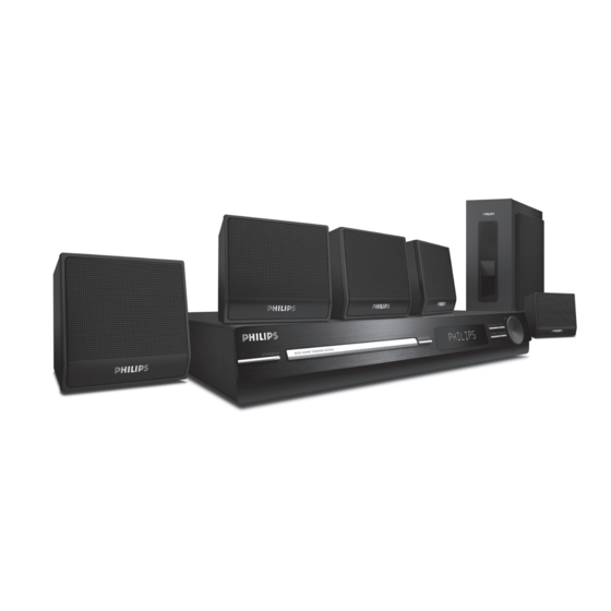
DVD Home Theater System
Service
Service Manual
This service manual is for HTS3011/98 Second Generation
model, which is different from the previous generation
HTS3011/98 models.
For Second Generation model the serial number begin with
MF2AXXXXXXXXXX. Refer to the rating label illustration at right.
©
Copyright 2008 Philips Consumer Electronics B.V. Eindhoven, The Netherlands
All rights reserved. No part of this publication may be reproduced, stored in a retrieval system or
transmitted, in any form or by any means, electronic, mechanical, photocopying, or otherwise
without the prior permission of Philips.
Published by
LM0832
Service Audio Printed in The Netherlands Subject to modification
Version 1.0
Second Generation
TABLE OF CONTENTS
Location of PCB Boards ............................................ 1-2
Versions Variation ...................................................... 1-2
Specifications ............................................................ 1-3
Measurement Setup .................................................. 1-4
Service Aids .............................................................. 1-5
ESD & Safety Instruction .......................................... 1-6
Lead-free solding Information .................................... 1-7
Setting procedure & Repair Instructions........................ 2
Disassembly Instructions & Service positions .............. 3
Block & Wiring Diagram ................................................ 4
VFD+STANDBY+VOL+MP3+BRACKET Board ............ 5
Main Board .................................................................... 6
Power Board .................................................................. 7
Mechanical Exploded View & Part List .......................... 8
Revision List .................................................................. 9
1 - 1
Chapter
HTS3011
/98
GB
3139 785 34480
Advertisement

Related Manuals for Philips HTS3011-Mk2


Summary of Contents for Philips HTS3011-Mk2
- Page 1 MF2AXXXXXXXXXX. Refer to the rating label illustration at right. © Copyright 2008 Philips Consumer Electronics B.V. Eindhoven, The Netherlands All rights reserved. No part of this publication may be reproduced, stored in a retrieval system or transmitted, in any form or by any means, electronic, mechanical, photocopying, or otherwise without the prior permission of Philips.
- Page 2 1 - 2 LOCATION OF PCB BOARDS VERSION VARIATION: Type/Versions HTS3011 Features Output Power - 200W Voltage (110V~240V) Aux In SERVICE SCNARIO MATRIX: HTS3011 Type/Versions Board in used Main Board Power Board VFD+STANDBY+VOL+MP3+BRACKETBoard *C = Component Level Repair...
- Page 3 1 - 3 SPECIFICATIONS FRONT AND REAR SPEAKERS AMPLIFIER System ............Full range satellite Total output power : Impedance ................4 - Home Theatre mode ............. 200 W Speaker drivers .........3” full range speaker Frequency Response ......180 Hz – 18 kHz / ±3 dB Frequency response ........150 Hz –...
- Page 4 1 - 4 MEASUREMENT SETUP Tuner FM Bandpass LF Voltmeter 250Hz-15kHz e.g. PM2534 e.g. 7122 707 48001 RF Generator e.g. PM5326 S/N and distortion meter e.g. Sound Technology ST1700B Use a bandpass filter to eliminate hum (50Hz, 100Hz) and disturbance from the pilottone (19kHz, 38kHz). Use Audio Signal Disc SBC429 4822 397 30184 (replaces test disc 3)
- Page 5 1 - 5 SERVICE AIDS Service Tools: Universal Torx driver holder .........4822 395 91019 Torx bit T10 150mm ...........4822 395 50456 Torx driver set T6-T20 .........4822 395 50145 Torx driver T10 extended ........4822 395 50423 Compact Disc: SBC426/426A Test disc 5 + 5A ......4822 397 30096 SBC442 Audio Burn-in test disc 1kHz ....4822 397 30155 SBC429 Audio Signals disc .........4822 397 30184 Dolby Pro-logic Test Disc ........4822 395 10216...
- Page 6 1 - 6...
- Page 7 1 - 7...
- Page 8 2 - 1 2 - 1 System , Region Code , etc. Setting Produre 1)System Reset 7) Upgrading new sofeware a) Press “OPTIONS“ button on R/C,TV will show setup menu a) copy “sofeware les” into a CD-R b) Select the menu using the on R/C b) open the CD Door,then insert the CD-R program disc c) Go preference page to do system reset...
- Page 9 2 - 2 2 - 2 REPAIR INSTRUCTIONS Chang F901 Ok or No Check CHANG D902/903/904/908 D902/903/904/908 D909/911/912 D909/911/912 OK or No Check Repair IC901/IC902/IC903 /Q902 or output circuit...
- Page 10 3 - 1 3 - 1 DISASSEMBLY INSTRUCTIONS Dismantling of the Front Panel Assemble 3) Loosen 5 screws and remove the Top Cover by lifting the rear portion upwards before sliding it out towards the rear. - 1 screw “A” each on the left & right side as shown in gure 4. 1) Open the DVD Tray by using the Open/Close Button while the Set is ON and disconnect the mains supply after removing the Tray - 3 screws “B”...
- Page 11 3 - 2 3 - 2 Dismantling of the DVD Module Dismantling of the Main Board 1) Loosen 4 screws “ E “ at the DVD Module as shown in gure 8. 1) Loosen 4 screws “H” on the top of Main Board as shown in gure 11. 2) Loosen 4 screws “I”...
- Page 12 4 - 1 4 - 1 BLOCK DIAGRAM...
- Page 13 4 - 2 4 - 2 WIRING DIAGRAM...
- Page 14 5 - 1 5 - 1 FTD DISPLAY PIN ASSIGNMENT CONTROL BOARD TABLE OF CONTENTS FTD Display Pin Assignment ............. 5-1 Circuit Diagram ................. 5-2 PCB Layout Top View ............... 5-3 PCB Layout Bottom View ..............5-4 PIN CONNECTION...
- Page 15 5 - 2 5 - 2 CIRCUIT DIAGRAM C200 A2 R202 A2 C201 A2 R203 B2 C202 B2 R204 B2 C203 C2 R205 B2 C204 B2 R206 C1 C205 B1 R207 C1 C206 C2 R208 D1 C207 C1 R209 D1 C208 B2 R210 D4 C209 B2...
- Page 16 5 - 3 5 - 3 PCB LAYOUT - TOP VIEW C208 D203 JW10 JW15 JW19 JW22 R202 R214 RB201 C3 TA201 B4 TA205 A1 C209 DP200 B2 JW12 JW16 JW23 LD200 A1 R203 R215 RB204 C2 TA202 C1 VR200 A3 C216 JW13 JW17...
- Page 17 5 - 4 5 - 4 PCB LAYOUT - BOTTOM VIEW C200 C204 C210 C214 C219 C226 D201 R205 R209 R218 ZD202 A4 C201 C205 C211 C215 C220 C288 IC200 B3 R206 R210 R225 ZD203 C2 C202 C206 C212 C217 C221 C289 Q200 B4...
- Page 18 6 - 1 6 - 1 INTERNAL IC DIAGRAM - MT1389HD Debug 108MHz CVBS,Y/C CVBS,Y/C Module Port Component Component RF Amplifier TV Encoder Video Video Motor Servo IO Video DAC Servo Drive Spindle Processor Control Video digital video RASH Processor Interlacer Memory Audio...
- Page 19 6 - 2 6 - 2 CIRCUIT DIAGRAM - part one C1001 A4 C182 C4 C421 B3 C801 B2 D614 C4 Q401 A3 R325 A1 R617 C4 C1002 A4 C183 C4 C422 B3 C802 B2 D615 C4 Q402 B3 R326 A1 R618 C4 C1003 A4 C184 C4...
- Page 20 6 - 3 6 - 3 PCB LAYOUT - TOP VIEW C1011 C4 C159 B1 C332 A2 C367 C4 C439 B3 C538 C5 C571 C4 C816 C1 C845 C2 D104 C3 FB1101 A1 FB802 C3 JK1103A L511 A4 R108 C2 R147 B1 R302 A3 R335 A3...
- Page 21 6 - 4 6 - 4 PCB LAYOUT - BOTTOM VIEW C1001 B4 C1010 B3 C1023 A4 C1106 A5 C118 C3 C135 B5 C182 C3 C303 A3 C368 A2 C408 B4 C435 C2 C545 B2 C603 A1 C809 B5 C848 B4 C902 A3 D619 A2 R114 C4...
- Page 22 7 - 1 7 - 1 INTERNAL IC DIAGRAM - AP3843GMTR UVLO 2.50V INTERNAL BIAS VREF GOOD OUTPUT LOGIC POWER BOARD OVER TEMP PROTECT ERROR COMP LATCH CURRENT SENSE COMPARATOR TABLE OF CONTENTS Internal IC Diagram ................7-1 Circuit Diagram .................. 7-2 PCB Layout Top View ...............
- Page 23 7 - 2 7 - 2 CIRCUIT DIAGRAM BD901 A1 C909 C917 C925 C933 C942 CN902 A4 D908 GT901 B1 L903 Q905 R906 R914 R924 R932 R942 R955 C901 C910 C918 C926 C934 C943 CN903 B4 D909 GT902 B1 L904 Q908 R907 R915...
- Page 24 7 - 3 7 - 3 PCB LAYOUT - TOP VIEW BD901 A1 C910 C923 C929 C943 CN902 B4 D904 D913 IC903 J911 L904 Q904 R908 R932 C901 C911 C924 C930 C946 CN903 D3 D905 F901 J904 J912 L905 Q905 R915 R933 C902...
- Page 25 7 - 4 7 - 4 PCB LAYOUT - BOTTOM VIEW C904 C914 C919 C934 C942 IC901 R903 R909 R913 R923 R927 R934 R942 R947 R955 C905 C915 C922 C935 C945 J901 R904 R910 R914 R924 R928 R935 R943 R948 R956 C908 C916...
- Page 26 8 - 1 8 - 1 Mechanical Exploded View Note: A1=18+13+17+34+35...
- Page 27 8- 2 8 - 2 MECHANICAL PART LIST Loc. 12NC No. Description Loc. 12NC No. Description Loc. 12NC No. Description MAIN IC501 996510012541 IC 36P STA518 PSSO ST 40V 3.5A CN901 996500019399 CONNECTOR 3P CL3962WVO IC502 996510012541 IC 36P STA518 PSSO ST 40V 3.5A CN902 996500015863 CONNECTOR B5B-XH-A 5 PIN...
- Page 28 9 - 1 9 - 1 REVISION LIST Version 1.0 *Initial release...