Table of Contents
Advertisement
Quick Links
Advertisement
Table of Contents

Related Manuals for National Instruments 6368


Summary of Contents for National Instruments 6368
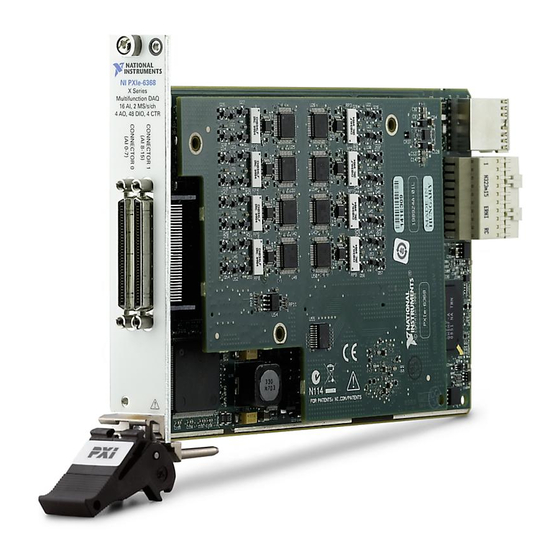
- Page 1 PXIe-6368...
- Page 2 DAQ X Series X Series User Manual NI 632x/634x/635x/636x/637x/638x/639x Devices X Series User Manual Français Deutsch ni.com/manuals May 2019 370784K-01...
- Page 3 11500 North Mopac Expressway Austin, Texas 78759-3504 USA Tel: 512 683 0100 For further support information, refer to the NI Services appendix. To comment on NI documentation, refer to the NI website at and enter the Info Code ni.com/info feedback © 2009–2019 National Instruments. All rights reserved.
- Page 4 National Instruments Corporation. National Instruments respects the intellectual property of others, and we ask our users to do the same. NI software is protected by copyright and other intellectual property laws. Where NI software may be used to reproduce software or other materials belonging to others, you may use NI software only to reproduce materials that you may reproduce in accordance with the terms of any applicable license or other legal restriction.
- Page 5 ™ The ExpressCard word mark and logos are owned by PCMCIA and any use of such marks by National Instruments is under license. The mark LabWindows is used under a license from Microsoft Corporation. Windows is a registered trademark of Microsoft Corporation in the United States and other countries.
-
Page 6: Table Of Contents
SCXI Accessories ..................... 2-4 SCC Accessories....................2-4 BNC Accessories....................2-5 Screw Terminal Accessories ................2-6 RTSI Cables...................... 2-6 Cables ....................... 2-6 Custom Cabling and Connectivity..............2-7 USB Device Accessories, USB Cable, Power Supply, and Ferrite....2-7 © National Instruments | v... - Page 7 Contents Signal Conditioning ......................2-8 Sensors and Transducers...................2-8 Signal Conditioning Options ..................2-9 SCXI ......................... 2-9 SCC........................2-9 Programming Devices in Software ................... 2-10 Chapter 3 Connector and LED Information I/O Connector Signal Descriptions ................... 3-2 +5 V Power Source ......................3-5 USER 1 and USER 2 ......................
- Page 8 AI Sample Clock Timebase Signal..............4-49 AI Hold Complete Event Signal............... 4-50 AI Start Trigger Signal ..................4-50 AI Reference Trigger Signal................4-53 AI Pause Trigger Signal ................... 4-54 Getting Started with AI Applications in Software............ 4-56 © National Instruments | vii...
- Page 9 Contents Chapter 5 Analog Output AO Reference Selection....................5-2 Minimizing Glitches on the Output Signal ...............5-2 Analog Output Data Generation Methods ................ 5-3 Software-Timed Generations ..................5-3 Hardware-Timed Generations................... 5-3 Analog Output Triggering ....................5-4 Connecting Analog Output Signals .................. 5-5 Analog Output Timing Signals ..................
- Page 10 Programmable Power-Up States..................6-18 DI Change Detection ......................6-19 DI Change Detection Applications................6-20 Digital Filtering ........................ 6-20 Watchdog Timer ....................... 6-23 Connecting Digital I/O Signals..................6-24 Getting Started with DIO Applications in Software............6-25 © National Instruments | ix...
- Page 11 Contents Chapter 7 Counters Counter Timing Engine ....................7-2 Counter Input Applications....................7-3 Counting Edges......................7-3 Single Point (On-Demand) Edge Counting ............7-4 Buffered (Sample Clock) Edge Counting............7-4 Controlling the Direction of Counting.............. 7-5 Pulse-Width Measurement..................7-5 Single Pulse-Width Measurement ..............7-6 Implicit Buffered Pulse-Width Measurement...........7-6 Sample Clocked Buffered Pulse-Width Measurement ........
- Page 12 Other Counter Features..................... 7-45 Cascading Counters ....................7-45 Prescaling........................7-46 Synchronization Modes .................... 7-46 100 MHz Source Mode..................7-47 External Source Greater than 25 MHz ............. 7-47 External or Internal Source Less than 25 MHz ..........7-47 © National Instruments | xi...
- Page 13 Contents Chapter 8 Using PFI Terminals as Timing Input Signals..............8-2 Exporting Timing Output Signals Using PFI Terminals ..........8-2 Using PFI Terminals as Static Digital I/Os ..............8-3 Using PFI Terminals to Digital Detection Events ............8-4 Connecting PFI Input Signals ...................8-4 PFI Filters .........................
- Page 14 NI USB-6343 Screw Terminal Pinout ..........A-9 Figure A-7. NI USB-6343 BNC Pinout ..............A-10 Figure A-8. NI PXIe-6345/6355 Pinout..............A-12 Figure A-9. NI PCIe-6346 Pinout ................A-14 Figure A-10. NI USB 6346 Screw Terminal Pinout........... A-15 © National Instruments | xiii...
- Page 15 NI USB-6356/6366 Screw Terminal Pinout.......... A-36 Figure A-25. NI USB-6356/6366 BNC Pinout ............A-37 Figure A-26. NI PXIe-6358/6368/6378 Pinout............A-39 Figure A-27. NI PXIe-6365 Connector 2 Pinout ............A-41 Figure A-28. NI PXIe-6365 Connector 0 and Connector 1 Pinout ......A-42 Figure A-29.
-
Page 16: Getting Started
Getting Started The X Series User Manual contains information about using the National Instruments X Series data acquisition (DAQ) devices with NI-DAQmx 19.0 and later. X Series devices feature up to 208 analog input (AI) channels, up to four analog output (AO) channels, up to 48 lines of digital input/output (DIO), and four counters. -
Page 17: Electromagnetic Compatibility Guidelines
At the end of the product life cycle, all products must be sent to a WEEE recycling center. For more information about WEEE recycling centers, National Instruments WEEE initiatives, and compliance with WEEE Directive 2002/96/EC on Waste and Electronic Equipment, visit ni.com/environment/... -
Page 18: Installation
Notify NI if the device appears damaged in any way. Do not install a damaged device in your computer or chassis. Store the device in the antistatic package when the device is not in use. © National Instruments | 1-3... -
Page 19: Device Self-Calibration
Chapter 1 Getting Started Device Self-Calibration NI recommends that you self-calibrate your X Series device after installation and whenever the ambient temperature changes. Self-calibration should be performed after the device has warmed up for the recommended time period. Refer to the device specifications to find your device warm-up time. -
Page 20: Getting Started With X Series Usb Devices
NI BNC USB-63xx device. Use as short a wire as possible. In addition, the wires in the shielded cable that extend beyond the shield should be as short as possible. Note (NI USB-636 Mass Termination Devices) USB Mass Termination X Series devices have chassis ground connection through the I/O connector. © National Instruments | 1-5... -
Page 21: Ferrite Installation
Chapter 1 Getting Started Ferrite Installation (NI USB-63 xx Mass Termination and BNC Devices) To ensure the specified EMC performance for radiated RF emissions of the NI USB-63xx Mass Termination and BNC device, install the included snap-on ferrite bead onto the power cable, as shown in Figure 1-2. Ensure that the ferrite bead is as close to the end of the power cable as practical. -
Page 22: Mounting Ni Usb X Series Devices
While holding the USB X Series device in place, attach the front bracket to the backpanel wall mount by tightening the two thumbscrews. © National Instruments | 1-7... -
Page 23: Din Rail Mounting
Chapter 1 Getting Started DIN Rail Mounting Complete the following steps to mount your USB X Series device to a DIN rail using the USB X Series mounting kit with DIN rail clip (part number 781515-01 not included in your USB X Series device kit). -
Page 24: Usb Device Leds
USB cable (included in the USB X Series device kit) to securely attach the cable to the device, as shown in Figure 1-6. Figure 1-6. USB Cable Strain Relief on USB X Series Devices Locking USB Cable Jackscrew Jackscrew Hole Security Cable Slot © National Instruments | 1-9... -
Page 25: Usb Device Security Cable Slot
Chapter 1 Getting Started USB Device Security Cable Slot (NI USB-63 Devices) The security cable slot, shown in Figure 1-6, allows you to attach an optional laptop lock to your USB X Series device. Note The security cable is designed to act as a deterrent, but might not prevent the device from being mishandled or stolen. -
Page 26: Daq System Overview
PC. The following sections cover the components of a typical DAQ system. Figure 2-1. Components of a Typical DAQ System Signal Cables and Personal Computer Conditioning Accessories Hardware Software Sensors and PXI Express Transducers Chassis © National Instruments | 2-1... -
Page 27: Daq Hardware
Chapter 2 DAQ System Overview DAQ Hardware DAQ hardware digitizes signals, performs D/A conversions to generate analog output signals, and measures and controls digital I/O signals. Figure 2-2 features components common to all X Series devices. Figure 2-2. General X Series Block Diagram Analog Input Analog Output Digital... -
Page 28: Calibration Circuitry
Refer to the Custom Cabling and Connectivity section of this chapter and the Field Wiring Considerations section of Chapter 4, Analog Input, for information about how to select accessories for your X Series device. © National Instruments | 2-3... -
Page 29: Pci Express, Pxi Express, And Usb Mass Termination Device Cables And Accessories
SCXI is a programmable signal conditioning system designed for measurement and automation applications. To connect your X Series device to an SCXI chassis, use the SCXI-1349 adapter and an SHC68-68-EPM cable. Note (NI 6346/6349/6356/6358/6366/6368/6374/6376/6378 Devices) Simultaneous MIO (SMIO) X Series devices only support controlling SCXI in parallel mode. -
Page 30: Bnc Accessories
24 differential analog inputs for connector 1 of the NI 6349 device. The BNC-2111 cannot be used with NI 6356/6358/6366/6368/6374/6376/6378/6386/6396 SMIO X Series devices. † The BNC-2115 can only be used on connectors 1, 2, or 3 of NI 6345/6355/6365/6375 devices and connector 1 of the NI 6349 device. -
Page 31: Screw Terminal Accessories
6355/6365/6375 devices and connector 1 of the NI 6349 device. Screw Terminal Accessories National Instruments offers several styles of screw terminal connector blocks. All terminal connector blocks require a cable except the TB-2706 to connect an X Series device to a connector block, as listed in Table 2-2. -
Page 32: Custom Cabling And Connectivity
NI offers a variety of products to use with the USB X Series devices, as shown in Table 2-3. NI recommends that you use the SHC68-68-EPM cable; however, an SHC68-68-EP cable works with X Series devices. © National Instruments | 2-7... -
Page 33: Signal Conditioning
Chapter 2 DAQ System Overview Table 2-3. USB Device Accessories, Power Supply, and Ferrite Description Part Number Universal power supply with mini-combicon 781513-01 connector, 12 VDC, 2.5 A USB X Series mounting kit with DIN rail clip* 781515-01 USB X Series mounting kit* 781514-01 USB X Series lid with thumbscrew fasteners 781661-01... -
Page 34: Signal Conditioning Options
SCXI is designed for large measurement systems or systems requiring high-speed acquisition. Note (NI 6346/6349/6356/6358/6366/6368/6374/6376/6378 Devices) Simultaneous MIO (SMIO) X Series devices only support controlling SCXI in parallel mode. -
Page 35: Programming Devices In Software
Simultaneous MIO (SMIO) X Series devices do not support SCC. Programming Devices in Software National Instruments measurement devices are packaged with NI-DAQmx driver software, an extensive library of functions and VIs you can call from your application software, such as LabVIEW or LabWindows/CVI, to program all the features of your NI measurement devices. - Page 36 NI-DAQmx 9.5 NI PXIe-6345/6355/6365/6375 NI-DAQmx 14.1 NI PXIe-6376/6378 NI-DAQmx 15.5 NI PCIe-6374/6376 NI-DAQmx 17.6 NI PXIe-6349 NI-DAQmx 18.1 NI PCIe-6346 NI-DAQmx 18.1 USB-6346/6349 Screw Terminal NI-DAQmx 18.6 USB-6346/6349 BNC NI-DAQmx 18.6 NI PXIe-6386/6396 NI-DAQmx 19.0 © National Instruments | 2-11...
-
Page 37: Connector And Led Information
RTSI Connector Pinout sections refer to X Series PCI Express device power and the RTSI connector on PCI Express devices. USB Device LED Patterns section refers to the X Series USB device READY, POWER, and ACTIVE LEDs. © National Instruments | 3-1... -
Page 38: I/O Connector Signal Descriptions
Chapter 3 Connector and LED Information I/O Connector Signal Descriptions Table 3-1 describes the signals found on the I/O connectors. Not all signals are available on all devices. Table 3-1. I/O Connector Signals Signal Name Reference Direction Description AI GND —... - Page 39 These functions are not available on all devices. Refer to the device specifications. +5 V D GND Output +5 V Power Source—These terminals provide a fused +5 V power source. Refer to the +5 V Power Source section for more information. © National Instruments | 3-3...
- Page 40 Chapter 3 Connector and LED Information Table 3-1. I/O Connector Signals (Continued) Signal Name Reference Direction Description PFI <0..7>/ D GND Input or Programmable Function Interface or Digital I/O P1.<0..7> Output Channels 0 to 7 and Channels 8 to 15—Each of PFI <8..15>/ these terminals can be individually configured as a P2.<0..7>...
-
Page 41: +5 V Power Source
Figure 3-1. USER 1 and USER 2 BNC Connections Screw Terminal Block Internal Connection USER 1 USER 1 BNC USER 2 D GND +5 V AI GND D GND AI SENSE AI SENSE 2 USER 2 BNC APFI 0 CHS GND D GND © National Instruments | 3-5... -
Page 42: Pci Express Device Disk Drive Power Connector
Chapter 3 Connector and LED Information PCI Express Device Disk Drive Power Connector (NI PCIe-632 /634 /635 /636 Devices, not including PCIe-6346) The disk drive power connector is a four-pin hard drive connector on some PCI Express devices that, when connected, increases the current the device can supply on the +5 V terminal. -
Page 43: Rtsi Connector Pinout
Detection can take 30 to 45 seconds. The device is configured, but there is no activity over the bus. The device is configured and there is activity over the bus. Blinking * USB BNC devices only. © National Instruments | 3-7... -
Page 44: Analog Input
• Analog Input on Simultaneous MIO X Series Devices—NI 6346/6349/6356/6358/6366/6368/6374/6376/6378/6386/6396 devices can be configured for differential analog input simultaneous sampled measurements. Analog Input on MIO X Series Devices Figure 4-1 shows the analog input circuitry of MIO X Series devices. -
Page 45: Analog Input Range
Chapter 4 Analog Input • Instrumentation Amplifier (NI-PGIA)—The NI programmable gain instrumentation amplifier (NI-PGIA) is a measurement and instrument class amplifier that minimizes settling times for all input ranges. The NI-PGIA can amplify or attenuate an AI signal to ensure that you use the maximum resolution of the ADC. MIO X Series devices use the NI-PGIA to deliver high accuracy even when sampling multiple channels with small input ranges at fast rates. -
Page 46: Working Voltage Range
The total working voltage of the positive input, which is equivalent to (Vcm + Vs), or subtracting AI GND from AI <0..x>+, must be less than ±11 V. If any of these conditions are exceeded, the input voltage is clamped until the fault condition is removed. © National Instruments | 4-3... -
Page 47: Analog Input Ground-Reference Settings
Chapter 4 Analog Input Analog Input Ground-Reference Settings MIO X Series devices support the following analog input ground-reference settings: • Differential mode—In DIFF mode, the MIO X Series device measures the difference in voltage between two AI signals. • Referenced single-ended mode—In RSE mode, the MIO X Series device measures the voltage of an AI signal relative to AI GND. - Page 48 For differential measurements, AI 0 and AI 8 are the positive and negative inputs of differential analog input channel 0. For a complete list of signal pairs that form differential input channels, refer to the I/O Connector Signal Descriptions section of Chapter 3, Connector and LED Information. © National Instruments | 4-5...
-
Page 49: Configuring Ai Ground-Reference Settings In Software
Chapter 4 Analog Input Caution The maximum input voltages rating of AI signals with respect to ground (and for signal pairs in differential mode with respect to each other) are listed in the device specifications. Exceeding the maximum input voltage of AI signals distorts the measurement results. - Page 50 The capacitance of the cable can also increase the settling time. National Instruments recommends using individually shielded, twisted-pair wires that are 2 m or less to connect AI signals to the device. Refer to the...
- Page 51 Chapter 4 Analog Input • Insert Grounded Channel between Signal Channels—Another technique to improve settling time is to connect an input channel to ground. Then insert this channel in the scan list between two of your signal channels. The input range of the grounded channel should match the input range of the signal after the grounded channel in the scan list.
-
Page 52: Analog Input Data Acquisition Methods
With continuous operations, if the user program does not read data out of the PC buffer fast enough to keep up with the data transfer, the buffer could reach an overflow condition, causing an error to be generated. © National Instruments | 4-9... -
Page 53: Analog Input Triggering
Chapter 4 Analog Input • Hardware-timed single point (HWTSP)—Typically, HWTSP operations are used to read single samples at known time intervals. While buffered operations are optimized for high throughput, HWTSP operations are optimized for low latency and low jitter. In addition, HWTSP can notify software if it falls behind hardware. - Page 54 Refer to the Analog Input Ground-Reference Settings section for descriptions of the RSE, NRSE, and DIFF modes and software considerations. † Refer to the Connecting Ground-Referenced Signal Sources section for more information. © National Instruments | 4-11...
-
Page 55: Connecting Floating Signal Sources
Chapter 4 Analog Input Connecting Floating Signal Sources What Are Floating Signal Sources? A floating signal source is not connected to the building ground system, but has an isolated ground-reference point. Some examples of floating signal sources are outputs of transformers, thermocouples, battery-powered devices, optical isolators, and isolation amplifiers. -
Page 56: When To Use Referenced Single-Ended (Rse) Connections With Floating Signal Sources
This connection works well for DC-coupled sources with low source impedance (less than 100 Ω). Note (NI USB-6341/6343/6346/6361/6363 BNC Devices) To measure a floating signal source on X Series USB BNC devices, move the switch under the BNC connector to the FS position. © National Instruments | 4-13... - Page 57 Chapter 4 Analog Input Figure 4-4. Differential Connections for Floating Signal Sources without Bias Resistors MIO X Series Device Floating Signal Source – AI– Inpedance AI SENSE <100 Ω AI GND However, for larger source impedances, this connection leaves the DIFF signal path significantly off balance.
- Page 58 (typically 100 kΩ to 1 MΩ). In this case, connect the negative input directly to AI GND. If the source has high output impedance, balance the © National Instruments | 4-15...
-
Page 59: Using Non-Referenced Single-Ended (Nrse) Connections For Floating Signal Sources
Chapter 4 Analog Input signal path as previously described using the same value resistor on both the positive and negative inputs; be aware that there is some gain error from loading down the source, as shown in Figure 4-7. Figure 4-7. Differential Connections for AC Coupled Floating Sources with Balanced Bias Resistors MIO X Series Device AC Coupling... -
Page 60: Using Referenced Single-Ended (Rse) Connections For Floating Signal Sources
1 and 100 mV, but the difference can be much higher if power distribution circuits are improperly connected. If a grounded signal source is incorrectly measured, this difference can appear as measurement error. Follow the connection instructions © National Instruments | 4-17... -
Page 61: When To Use Differential Connections With Ground-Referenced Signal Sources
Chapter 4 Analog Input for grounded signal sources to eliminate this ground potential difference from the measured signal. When to Use Differential Connections with Ground-Referenced Signal Sources Use DIFF input connections for any channel that meets any of the following conditions: •... -
Page 62: When To Use Referenced Single-Ended (Rse) Connections With Ground-Referenced Signal Sources
With this type of connection, the NI-PGIA rejects both the common-mode noise in the signal and the ground potential difference between the signal source and the device ground, shown as Vcm in the figure. AI+ and AI- must both remain within ±11 V of AI GND. © National Instruments | 4-19... -
Page 63: Using Non-Referenced Single-Ended (Nrse) Connections For Ground-Referenced Signal Sources
Chapter 4 Analog Input Using Non-Referenced Single-Ended (NRSE) Connections for Ground-Referenced Signal Sources Figure 4-11 shows how to connect ground-reference signal sources in NRSE mode. Figure 4-11. Single-Ended Connections for Ground-Referenced Signal Sources (NRSE Configuration) I/O Connector AI <0..x> Ground- Referenced Signal Instrumentation... -
Page 64: Field Wiring Considerations
Refer to the Field Wiring and Noise Considerations for Analog Signals document, for more information. To access this document, go to and enter the Info Code ni.com/info rdfwn3 © National Instruments | 4-21... -
Page 65: Analog Input Timing Signals
Chapter 4 Analog Input Analog Input Timing Signals In order to provide all of the timing functionality described throughout this section, MIO X Series devices have a flexible timing engine. Figure 4-12 summarizes all of the timing options provided by the analog input timing engine. Also refer to the Clock Routing section of Chapter 9, Digital Routing and Clock... - Page 66 MIO X Series devices feature the following analog input timing signals: • AI Sample Clock Signal • AI Sample Clock Timebase Signal • AI Convert Clock Signal • AI Convert Clock Timebase Signal © National Instruments | 4-23...
-
Page 67: Aggregate Versus Single Channel Sample Rates
Chapter 4 Analog Input • AI Hold Complete Event Signal • AI Start Trigger Signal • AI Reference Trigger Signal • AI Pause Trigger Signal Signals with an support digital filtering. Refer to the PFI Filters section of Chapter 8, PFI, for more information. - Page 68 When using the AI timing engine, you can also specify a configurable delay from AI Start Trigger to the first AI Sample Clock pulse. By default, this delay is set to four ticks of the AI Sample Clock Timebase signal. © National Instruments | 4-25...
-
Page 69: Ai Sample Clock Timebase Signal
Chapter 4 Analog Input When using an externally generated AI Sample Clock, you must ensure the clock signal is consistent with respect to the timing requirements of AI Convert Clock. Failure to do so may result in a scan overrun and will cause an error. Refer to the AI Convert Clock Signal section for more information about the timing requirements between AI Convert Clock and AI Sample... -
Page 70: Ai Convert Clock Signal
It then reloads itself in preparation for the next AI Sample Clock pulse. Several other internal signals can be routed to AI Convert Clock through internal routes. Refer to Device Routing in MAX in the NI-DAQmx Help or the LabVIEW Help for more information. © National Instruments | 4-27... - Page 71 Chapter 4 Analog Input Using an External Source Use one of the following external signals as the source of AI Convert Clock: • PFI <0..15> • RTSI <0..7> • PXI_STAR • PXIe_DSTAR<A,B> • Analog Comparison Event (an analog trigger) Routing AI Convert Clock Signal to an Output Terminal You can route AI Convert Clock (as an active low signal) out to any PFI <0..15>, RTSI <0..7>, or PXIe_DSTARC terminal.
- Page 72 Sample #3 Figure 4-21. AI Sample Clock and AI Convert Clock Properly Matched AI Sample Clock AI Convert Clock Channel Measured 1 2 3 1 2 3 1 2 3 Sample #1 Sample #2 Sample #3 © National Instruments | 4-29...
-
Page 73: Ai Convert Clock Timebase Signal
Chapter 4 Analog Input AI Convert Clock Timebase Signal The AI Convert Clock Timebase (ai/ConvertClockTimebase) signal is divided down to provide one of the possible sources for AI Convert Clock. Use one of the following signals as the source of AI Convert Clock Timebase: •... - Page 74 You can also specify whether the measurement acquisition begins on the rising edge or falling edge of AI Start Trigger. Using an Analog Source When you use an analog trigger source, the acquisition begins on the first rising edge of the Analog Comparison Event signal. © National Instruments | 4-31...
-
Page 75: Ai Reference Trigger Signal
Chapter 4 Analog Input Routing AI Start Trigger to an Output Terminal You can route AI Start Trigger out to any PFI <0..15>, RTSI <0..7>, or PXIe_DSTARC terminal. The output is an active high pulse. All PFI terminals are configured as inputs by default. - Page 76 Routing AI Reference Trigger Signal to an Output Terminal You can route AI Reference Trigger out to any PFI <0..15>, RTSI <0..7>, PXI_Trig <0..7>, or PXIe_DSTARC terminal. All PFI terminals are configured as inputs by default. © National Instruments | 4-33...
-
Page 77: Ai Pause Trigger Signal
Chapter 4 Analog Input AI Pause Trigger Signal Use the AI Pause Trigger (ai/PauseTrigger) signal to pause and resume a measurement acquisition. The internal sample clock pauses while the external trigger signal is active and resumes when the signal is inactive. You can program the active level of the pause trigger to be high or low, as shown in Figure 4-24. -
Page 78: Getting Started With Ai Applications In Software
To locate LabVIEW, LabWindows/CVI, Measurement Studio, Visual Basic, and ANSI C examples, refer to the document, Where Are NI-DAQmx Examples Installed in Windows?, by going to and entering the Info Code ni.com/info daqmxexp For additional examples, refer to ni.com/examples © National Instruments | 4-35... -
Page 79: Analog Input On Simultaneous Mio X Series Devices
Chapter 4 Analog Input Analog Input on Simultaneous MIO X Series Devices Figure 4-25 shows the analog input circuitry of the Simultaneous MIO X Series devices. Figure 4-25. Simultaneous MIO X Series Analog Input Circuitry NI-PGIA – AI Data AI FIFO –... -
Page 80: Analog Input Terminal Configuration
Choosing a smaller input range improves the voltage resolution, but may result in the input signal going out of range. For more information about setting ranges, refer to the NI-DAQmx Help or the LabVIEW Help. © National Instruments | 4-37... -
Page 81: Working Voltage Range
Nominal Resolution Assuming X Series Device Input Range 5% Over Range 320 μV NI 6346/6349/6356/6358/ -10 V to 10 V 6366/6368/6374/ 160 μV -5 V to 5 V 6376/6378/6386/6396 64 μV -2 V to 2 V 32 μV -1 V to 1 V... - Page 82 PC buffer fast enough to keep up with the data transfer, the buffer could reach an overflow condition, causing an error to be generated. © National Instruments | 4-39...
-
Page 83: Analog Input Triggering
Chapter 4 Analog Input – Hardware-timed single point (HWTSP)—Typically, HWTSP operations are used to read single samples at known time intervals. While buffered operations are optimized for high throughput, HWTSP operations are optimized for low latency and low jitter. In addition, HWTSP can notify software if it falls behind hardware. These features make HWTSP ideal for real time control applications. -
Page 84: Connecting Analog Input Signals
The difference in ground potential between two instruments connected to the same building power system is typically between 1 mV and 100 mV, but the difference can be much © National Instruments | 4-41... -
Page 85: Differential Connections For Ground-Referenced Signal Sources
Chapter 4 Analog Input higher if power distribution circuits are improperly connected. If a grounded signal source is incorrectly measured, this difference can appear as measurement error. Follow the connection instructions for grounded signal sources to eliminate this ground potential difference from the measured signal. -
Page 86: Differential Connections For Floating Signal Sources
Low Source Impedance—You must reference the source to AI GND. The easiest way to make this reference is to connect the positive side of the signal to the positive input of the instrumentation amplifier and connect the negative side of the signal to AI GND as well as © National Instruments | 4-43... -
Page 87: Unused Channels
Chapter 4 Analog Input to the negative input of the instrumentation amplifier, without using resistors. This connection works well for DC-coupled sources with low source impedance (less than 100 Ω). • High Source Impedance—For larger source impedances, this connection leaves the DIFF signal path significantly off balance. -
Page 88: Minimizing Drift In Differential Mode
Simultaneous MIO X Series devices use AI Sample Clock (ai/SampleClock) to perform simultaneous sampling on all active analog channels. Since there is one ADC per channel, AI Sample Clock controls the sample period on all the channels in the task. © National Instruments | 4-45... - Page 89 Chapter 4 Analog Input An acquisition with posttrigger data allows you to view data that is acquired after a trigger event is received. A typical posttrigger DAQ sequence is shown in Figure 4-28. The sample counter is loaded with the specified number of posttrigger samples, in this example, five. The value decrements with each pulse on AI Sample Clock, until all desired samples have been acquired.
-
Page 90: Aggregate Versus Single Channel Sample Rates
NI 6366 2 MS/s 16 MS/s NI 6368 2 MS/s 32 MS/s NI 6374 3.57 MS/s 14.28 MS/s NI 6376 3.57 MS/s 28.56 MS/s NI 6378 3.57 MS/s 57.12 MS/s NI 6386 14.29 MS/s 114.29 MS/s © National Instruments | 4-47... -
Page 91: Ai Sample Clock Signal
Chapter 4 Analog Input Table 4-8. Analog Input Rates for Simultaneous MIO X Series Devices (Continued) Analog Input Rate Simultaneous MIO X Series Device Single Channel Total Aggregate NI 6396 14.29 MS/s 114.29 MS/s NI PXIe-6386/6396 devices support the listed analog input rates when using an internal clock. When using an externally-derived clock, the maximum single channel analog input rate is 15 MS/s and the total aggregate rate is 120 MS/s. -
Page 92: Ai Sample Clock Timebase Signal
Delay From Start Trigger AI Sample Clock Timebase Signal You can route any of the following signals to be the AI Sample Clock Timebase (ai/SampleClockTimebase) signal: • 100 MHz Timebase (default) • 20 MHz Timebase © National Instruments | 4-49... -
Page 93: Ai Hold Complete Event Signal
Chapter 4 Analog Input • 100 kHz Timebase • PXI_CLK10 • RTSI <0..7> • PFI <0..15> • PXI_STAR • PXIe_DSTAR<A,B> • Analog Comparison Event (an analog trigger) Note (NI PXIe-6386/6396 Devices) PXIe-6386 and PXIe-6396 devices differ in several ways from other SMIO devices. For more information about these devices related to AI Sample Clocks, go to and enter the Info Code ni.com/info... - Page 94 Figure 4-31. Simultaneous MIO X Series Retriggerable Analog Input AI Start Trigger AI Sample Clock Note Waveform information from LabVIEW does not reflect the delay between triggers. They are treated as a continuous acquisition with constant t0 and t1 information. © National Instruments | 4-51...
- Page 95 Chapter 4 Analog Input Note (NI USB-6356/6366 and PXIe-6378 Devices) Some X Series devices internally transfer data in sample pairs, as opposed to single samples. This implementation allows for greater data throughput. However, if an acquisition on these devices acquires an odd number of total samples, the last sample acquired cannot be transferred.
-
Page 96: Ai Reference Trigger Signal
When the reference trigger occurs, the DAQ device continues to write samples to the buffer until the buffer contains the number of posttrigger samples desired. Figure 4-32 shows the final buffer. Figure 4-32. Reference Trigger Final Buffer Reference Trigger Pretrigger Samples Posttrigger Samples Complete Buffer © National Instruments | 4-53... -
Page 97: Ai Pause Trigger Signal
Chapter 4 Analog Input Using a Digital Source To use AI Reference Trigger with a digital source, specify a source and an edge. The source can be any of the following signals: • PFI <0..15> • RTSI <0..7> • PXI_STAR •... - Page 98 DO Pause Trigger (do/PauseTrigger) The source can also be one of several other internal signals on your DAQ device. Refer to Device Routing in MAX in the NI-DAQmx Help or the LabVIEW Help for more information. © National Instruments | 4-55...
-
Page 99: Getting Started With Ai Applications In Software
Using an Analog Source When you use an analog trigger source, the internal sample clock pauses when the Analog Comparison Event signal is low and resumes when the signal goes high (or vice versa). Routing AI Pause Trigger Signal to an Output Terminal You can route AI Pause Trigger out to any PFI <0..15>, RTSI <0..7>, PXI_STAR, or PXIe_DSTARC terminal. -
Page 100: Analog Output
AO Sample Clock—The AO Sample Clock signal reads a sample from the DAC FIFO and generates the AO voltage. • AO Reference Selection—The AO reference selection signal allows you to change the range of the analog outputs. © National Instruments | 5-1... -
Page 101: Ao Reference Selection
Chapter 5 Analog Output AO Reference Selection AO reference selection allows you to set the analog output range. The analog output range describes the set of voltages the device can generate. The digital codes of the DAC are spread evenly across the analog output range. So, if the range is smaller, the analog output has better resolution;... -
Page 102: Analog Output Data Generation Methods
FIFO using DMA before it is written to the DACs one sample at a time. Buffered generation typically allow for much faster transfer rates than non-buffered acquisitions because data is moved in large blocks, rather than one point at a time. © National Instruments | 5-3... -
Page 103: Analog Output Triggering
Chapter 5 Analog Output One property of buffered I/O operations is the sample mode. The sample mode can be either finite or continuous: – Finite sample mode generation refers to the generation of a specific, predetermined number of data samples. Once the specified number of samples has been written out, the generation stops. -
Page 104: Connecting Analog Output Signals
100 kHz Timebase PXI_CLK10 X Series devices feature the following analog output (waveform generation) timing signals: • AO Start Trigger Signal • AO Pause Trigger Signal • AO Sample Clock Signal • AO Sample Clock Timebase Signal © National Instruments | 5-5... -
Page 105: Ao Start Trigger Signal
Chapter 5 Analog Output Signals with an support digital filtering. Refer to the PFI Filters section of Chapter 8, PFI, for more information. AO Start Trigger Signal Use the AO Start Trigger (ao/StartTrigger) signal to initiate a waveform generation. If you do not use triggers, you can begin a generation with a software command. -
Page 106: Using An Analog Source
Figure 5-6. Figure 5-6. AO PauseTrigger with Other Signal Source Pause Trigger Sample Clock © National Instruments | 5-7... -
Page 107: Using A Digital Source
Chapter 5 Analog Output Using a Digital Source To use AO Pause Trigger, specify a source and a polarity. The source can be one of the following signals: • PFI <0..15> • RTSI <0..7> • PXI_STAR • PXIe_DSTAR<A,B> • Counter n Internal Output •... -
Page 108: Using An External Source
Figure 5-7 shows the relationship of AO Sample Clock to AO Start Trigger. Figure 5-7. AO Sample Clock and AO Start Trigger AO Sample Clock Timebase AO Start Trigger AO Sample Clock Delay From Start Trigger © National Instruments | 5-9... -
Page 109: Ao Sample Clock Timebase Signal
Chapter 5 Analog Output AO Sample Clock Timebase Signal The AO Sample Clock Timebase (ao/SampleClockTimebase) signal is divided down to provide a source for AO Sample Clock. You can route any of the following signals to be the AO Sample Clock Timebase signal: •... -
Page 110: Getting Started With Ao Applications In Software
To locate LabVIEW, LabWindows/CVI, Measurement Studio, Visual Basic, and ANSI C examples, refer to the document, Where Are NI-DAQmx Examples Installed in Windows?, by going to and entering the Info Code ni.com/info daqmxexp For additional examples, refer to ni.com/examples © National Instruments | 5-11... -
Page 111: Digital I/O
P0. x I/O Protection DO. x Direction Control Weak Pull-Down Static DI DI Waveform Filter Measurement FIFO DI Sample Clock DI Change Detection The DIO terminals are named P0.<0..31> on the X Series device I/O connector. © National Instruments | 6-1... -
Page 112: Digital Input Data Acquisition Methods
Chapter 6 Digital I/O The voltage input and output levels and the current drive levels of the DIO lines are listed in the device specifications. Digital Input Data Acquisition Methods When performing digital input measurements, you either can perform software-timed or hardware-timed acquisitions. -
Page 113: Digital Input Triggering
An analog or digital trigger can initiate these actions. All X Series devices support digital triggering, but some do not support analog triggering. To find your device triggering options, refer to the device specifications. © National Instruments | 6-3... -
Page 114: Digital Waveform Acquisition
Chapter 6 Digital I/O Digital Waveform Acquisition Figure 6-2 summarizes all of the timing options provided by the digital input timing engine. Figure 6-2. Digital Input Timing Options DSTAR <A..B> 100 MHz Timebase PFI, RTSI DSTAR <A..B> PXI_STAR DI Sample Clock Analog Comparison Event PFI, RTSI Revamp AO timing options with DI timebase and clocks... -
Page 115: Using An Internal Source
DAQ device to ignore DI Sample Clock using the DI Pause Trigger signal. The DI timing engine on your device internally generates DI Sample Clock unless you select an external source. DI Start Trigger starts the timing engine and either software or hardware can © National Instruments | 6-5... -
Page 116: Di Sample Clock Timebase Signal
Chapter 6 Digital I/O stop it once a finite acquisition completes. When using the DI timing engine, you can also specify a configurable delay from DI Start Trigger to the first DI Sample Clock pulse. By default, this delay is set to two ticks of the DI Sample Clock Timebase signal. Figure 6-3. -
Page 117: Di Start Trigger Signal
To use DI Start Trigger with a digital source, specify a source and an edge. The source can be any of the following signals: • PFI <0..15> • RTSI <0..7> • Counter n Internal Output © National Instruments | 6-7... -
Page 118: Using An Analog Source
Chapter 6 Digital I/O • PXI_STAR • PXIe_DSTAR<A,B> • Change Detection Event • AI Start Trigger (ai/StartTrigger) • AO Start Trigger (ao/StartTrigger) • DO Start Trigger (do/StartTrigger) The source can also be one of several other internal signals on your DAQ device. Refer to Device Routing in MAX in the NI-DAQmx Help or the LabVIEW Help for more information. -
Page 119: Using A Digital Source
Routing DI Reference Trigger Signal to an Output Terminal You can route DI Reference Trigger out to any PFI <0..15>, RTSI <0..7>, PXI_Trig <0..7>, or PXIe_DSTARC terminal. All PFI terminals are configured as inputs by default. © National Instruments | 6-9... -
Page 120: Di Pause Trigger Signal
Chapter 6 Digital I/O DI Pause Trigger Signal You can use the DI Pause Trigger (di/PauseTrigger) signal to pause and resume a measurement acquisition. The internal sample clock pauses while the external trigger signal is active and resumes when the signal is inactive. You can program the active level of the pause trigger to be high or low, as shown in Figure 6-6. -
Page 121: Routing Di Pause Trigger Signal To An Output Terminal
Lateness Checking document for more information. To access this document, go to and enter the Info Code ni.com/info daqhwtsp Note (NI USB-634 /635 /636 Devices) USB X Series devices do not support hardware-timed single point (HWTSP) operations. © National Instruments | 6-11... -
Page 122: Digital Output Triggering
Chapter 6 Digital I/O • Buffered—In a buffered generation, data is moved from a PC buffer to the DAQ device’s onboard FIFO using DMA before it is written to the output lines one sample at a time. Buffered generation typically allow for much faster transfer rates than non-buffered acquisitions because data is moved in large blocks, rather than one point at a time. -
Page 123: Digital Waveform Generation
One of the following internal signals can drive DO Sample Clock: • DI Sample Clock (di/SampleClock) • DO Sample Clock (do/SampleClock) • AI Sample Clock (ai/SampleClock) • AI Convert Clock (ai/ConvertClock) • AO Sample Clock (ao/SampleClock) • Counter n Sample Clock © National Instruments | 6-13... -
Page 124: Using An External Source
Chapter 6 Digital I/O • Counter n Internal Output • Frequency Output • DI Change Detection output Several other internal signals can be routed to DO Sample Clock through internal routes. Refer to Device Routing in MAX in the NI-DAQmx Help or the LabVIEW Help for more information. Using an External Source Use one of the following external signals as the source of DO Sample Clock: •... -
Page 125: Do Sample Clock Timebase Signal
After the clock generation is finished, the timing engine waits for another start trigger to begin another clock generation. Figure 6-8 shows a retriggerable DO of four samples. Figure 6-8. Retriggerable DO DO Start Trigger DO Sample Clock © National Instruments | 6-15... -
Page 126: Using A Digital Source
Chapter 6 Digital I/O Using a Digital Source To use DO Start Trigger, specify a source and an edge. The source can be one of the following signals: • A pulse initiated by host software • PFI <0..15> • RTSI <0..7> •... -
Page 127: Using A Digital Source
Routing in MAX in the NI-DAQmx Help or the LabVIEW Help for more information. You can also specify whether the samples are paused when DO Pause Trigger is at a logic high or low level. © National Instruments | 6-17... -
Page 128: Using An Analog Source
Chapter 6 Digital I/O Using an Analog Source When you use an analog trigger source, the samples are paused when the Analog Comparison Event signal is at a high level. Refer to the Triggering with an Analog Source section of Chapter 11, Triggering, for more information. -
Page 129: Di Change Detection
DI signal. The result of this OR is the Change Detection Event signal. Change detection performs bus correlation by considering all changes within a 50 ns window one change detection event, which keeps signals on the same bus synchronized in samples and prevents overruns. © National Instruments | 6-19... -
Page 130: Di Change Detection Applications
Chapter 6 Digital I/O The Change Detection Event signal can do the following: • Drive any RTSI <0..7>, PFI <0..15>, or PXI_STAR signal • Drive the DO Sample Clock or DI Sample Clock • Generate an interrupt The Change Detection Event signal can also be used to detect changes on digital output events. DI Change Detection Applications The DIO change detection circuitry can interrupt a user program when one of several DIO signals changes state. - Page 131 Case 1—If no transitions have occurred on the other lines, the transition propagates on the second filtered clock edge, as shown in Figure 6-13. Figure 6-13. Case 1 Stable Stable Stable Digital Input P0.A Digital Input P0.B Filter Clock Filtered Input A Filtered Input B © National Instruments | 6-21...
- Page 132 Chapter 6 Digital I/O • Case 2—If an additional line on the bus also has a transition during the filter clock period, the change is not propagated until the next filter clock edge, as shown in Figure 6-14. Figure 6-14. Case 2 Not Stable Not Stable Digital Input P0.A...
-
Page 133: Watchdog Timer
The counter on the watchdog timer is configurable up to - 1) × 8 ns (approximately 34 seconds) before it expires. A watchdog timer can be set for all DIO and PFI lines. © National Instruments | 6-23... -
Page 134: Connecting Digital I/O Signals
Chapter 6 Digital I/O Connecting Digital I/O Signals The DIO signals, P0.<0..31>, P1.<0..7>, and P2.<0..7> are referenced to D GND. You can individually program each line as an input or output. Figure 6-16 shows P1.<0..3> configured for digital input and P1.<4..7> configured for digital output. Figure 6-16 shows the switch receiving TTL signals and sensing external device states and shows the LED sending TTL signals and driving external devices. -
Page 135: Getting Started With Dio Applications In Software
To locate LabVIEW, LabWindows/CVI, Measurement Studio, Visual Basic, and ANSI C examples, refer to the document, Where Are NI-DAQmx Examples Installed in Windows?, by going to and entering the Info Code ni.com/info daqmxexp For additional examples, refer to ni.com/examples © National Instruments | 6-25... - Page 136 (Embedded Ctrn) for use in what are traditionally two-counter measurements and generations. The embedded counters cannot be programmed independent of the main counter; signals from the embedded counters are not routable. © National Instruments | 7-1...
-
Page 137: Counter Timing Engine
Chapter 7 Counters Counter Timing Engine Unlike analog input, analog output, digital input, and digital output, X Series counters do not have the ability to divide down a timebase to produce an internal counter sample clock. For sample clocked operations, an external signal must be provided to supply a clock source. The source can be any of the following signals: •... -
Page 138: Counter Input Applications
The counter values can be read on demand or with a sample clock. Refer to the following sections for more information about X Series edge counting options: • Single Point (On-Demand) Edge Counting • Buffered (Sample Clock) Edge Counting © National Instruments | 7-3... -
Page 139: Single Point (On-Demand) Edge Counting
Chapter 7 Counters Single Point (On-Demand) Edge Counting With single point (on-demand) edge counting, the counter counts the number of edges on the Source input after the counter is armed. On-demand refers to the fact that software can read the counter contents at any time without disturbing the counting process. -
Page 140: Controlling The Direction Of Counting
A pulse-width measurement is accurate even if the counter is armed while a pulse train is in progress. If a counter is armed while the pulse is in the active state, it waits for the next transition to the active state to begin the measurement. © National Instruments | 7-5... -
Page 141: Single Pulse-Width Measurement
Chapter 7 Counters Refer to the following sections for more information about X Series pulse-width measurement options: • Single Pulse-Width Measurement • Implicit Buffered Pulse-Width Measurement • Sample Clocked Buffered Pulse-Width Measurement • Hardware-Timed Single Point Pulse-Width Measurement Single Pulse-Width Measurement With single pulse-width measurement, the counter counts the number of edges on the Source input while the Gate input remains active. -
Page 142: Sample Clocked Buffered Pulse-Width Measurement
If a pulse does not occur between sample clocks, an overrun error occurs. Note (NI USB-634 /635 /636 Devices) USB X Series devices do not support hardware-timed single point (HWTSP) operations. For information about connecting counter signals, refer to the Default Counter/Timer Pins section. © National Instruments | 7-7... -
Page 143: Pulse Measurement
Chapter 7 Counters Pulse Measurement In pulse measurements, the counter measures the high and low time of a pulse on its Gate input signal after the counter is armed. A pulse is defined in terms of its high and low time, high and low ticks or frequency and duty cycle, which is similar to the pulse-width measurement, except that the inactive pulse is measured as well. -
Page 144: Sample Clocked Buffered Pulse Measurement
Note If a pulse does not occur between sample clocks, an overrun error occurs. Note (NI USB-634 /635 /636 Devices) USB X Series devices do not support hardware-timed single point (HWTSP) operations. © National Instruments | 7-9... -
Page 145: Pulse Versus Semi-Period Measurements
Chapter 7 Counters For information about connecting counter signals, refer to the Default Counter/Timer Pins section. Pulse versus Semi-Period Measurements In hardware, pulse measurement and semi-period are the same measurement. Both measure the high and low times of a pulse. The functional difference between the two measurements is how the data is returned. -
Page 146: Single Semi-Period Measurement
X Series frequency measurement options: • Low Frequency with One Counter • High Frequency with Two Counters • Large Range of Frequencies with Two Counters • Sample Clocked Buffered Frequency Measurement • Hardware-Timed Single Point Frequency Measurement © National Instruments | 7-11... -
Page 147: Low Frequency With One Counter
Chapter 7 Counters Low Frequency with One Counter For low frequency measurements with one counter, you measure one period of your signal using a known timebase. You can route the signal to measure (fx) to the Gate of a counter. You can route a known timebase (fk) to the Source of the counter. -
Page 148: Large Range Of Frequencies With Two Counters
The X Series device can measure this long pulse more accurately than the faster input signal. Note Counter 0 is always paired with Counter 1. Counter 2 is always paired with Counter 3. © National Instruments | 7-13... -
Page 149: Sample Clocked Buffered Frequency Measurement
Chapter 7 Counters You can route the signal to measure to the Source input of Counter 0, as shown in Figure 7-14. Assume this signal to measure has frequency fx. NI-DAQmx automatically configures Counter 0 to generate a single pulse that is the width of N periods of the source input signal. Figure 7-14. - Page 150 Figure 7-16. Sample Clocked Buffered Frequency Measurement (Non-Averaging) Counter Armed Gate Source Sample Clock Latched Values With sample clocked frequency measurements, ensure that the frequency to measure is twice as fast as the sample clock to prevent a measurement overflow. © National Instruments | 7-15...
-
Page 151: Hardware-Timed Single Point Frequency Measurement
Chapter 7 Counters Hardware-Timed Single Point Frequency Measurement Hardware-timed single point (HWTSP) frequency measurements can either be a single frequency measurement or an average between sample clocks. Use CI.Freq.EnableAveraging to set the behavior. For hardware-timed single point, the default is False. Refer to the Sample Clocked Buffered Frequency Measurement section for more information. - Page 152 ------------------------------ - --------------- ---- ------------------------- - fk fx N fk fx ---- 1 – – – Note: Accuracy equations do not take clock stability into account. Refer to your device specifications for clock stability. © National Instruments | 7-17...
- Page 153 Chapter 7 Counters Which Method Is Best? This depends on the frequency to be measured, the rate at which you want to monitor the frequency and the accuracy you desire. Take for example, measuring a 50 kHz signal. Assuming that the measurement times for the sample clocked (with averaging) and two counter frequency measurements are configured the same, Table 7-3 summarizes the results.
- Page 154 One of the disadvantages of a sample clocked frequency measurement is that the frequency to be measured must be at least twice the sample clock rate to ensure that a full period of the frequency to be measured occurs between sample clocks. © National Instruments | 7-19...
-
Page 155: Period Measurement
Chapter 7 Counters Table 7-5 summarizes some of the differences in methods of measuring frequency. Table 7-5. Frequency Measurement Method Comparison Measures Measures High Number of Number of Frequency Frequency Counters Measurements Signals Signals Method Used Returned Accurately Accurately Low frequency with Poor Good one counter... -
Page 156: Position Measurement
A, depending on which channel leads the other. Each cycle results in two increments or decrements, as shown in Figure 7-19. Figure 7-19. X2 Encoding Ch A Ch B Counter Value 5 © National Instruments | 7-21... - Page 157 Chapter 7 Counters • X4 Encoding—Similarly, the counter increments or decrements on each edge of channels A and B for X4 encoding. Whether the counter increments or decrements depends on which channel leads the other. Each cycle results in four increments or decrements, as shown in Figure 7-20.
-
Page 158: Measurements Using Two Pulse Encoders
Figure 7-23 shows an example of a buffered X1 position measurement. Figure 7-23. Buffered Position Measurement Counter Armed Sample Clock (Sample on Rising Edge) Ch A Ch B Count Buffer © National Instruments | 7-23... -
Page 159: Hardware-Timed Single Point Position Measurement
Chapter 7 Counters Hardware-Timed Single Point Position Measurement A hardware-timed single point (HWTSP) position measurement has the same behavior as a buffered (sample clock) position measurement. Note (NI USB-634 /635 /636 Devices) X Series USB devices do not support hardware-timed single point (HWTSP) operations. For information about connecting counter signals, refer to the Default Counter/Timer Pins section. -
Page 160: Implicit Buffered Two-Signal Edge-Separation Measurement
Aux signal. The counter then stores the count in the FIFO on a sample clock edge. On the next active edge of the Gate signal, the counter begins another measurement. A DMA controller transfers the stored values to host memory. © National Instruments | 7-25... -
Page 161: Hardware-Timed Single Point Two-Signal Separation Measurement
Chapter 7 Counters Figure 7-26 shows an example of a sample clocked buffered two-signal separation measurement. Figure 7-26. Sample Clocked Buffered Two-Signal Separation Measurement Sample Clock GATE SOURCE Counter Value Buffer Hardware-Timed Single Point Two-Signal Separation Measurement A hardware-timed single point (HWTSP) two-signal separation measurement has the same behavior as a sample clocked buffered two-signal separation measurement. -
Page 162: Simple Pulse Generation
Start Trigger to the beginning of the pulse. You can also specify the pulse width. The delay and pulse width are measured in terms of a number of active edges of the Source input. After the Start Trigger signal pulses once, the counter ignores the Gate input. © National Instruments | 7-27... -
Page 163: Pulse Train Generation
Chapter 7 Counters Figure 7-28 shows a generation of a pulse with a pulse delay of four and a pulse width of three (using the rising edge of Source). Figure 7-28. Single Pulse Generation with Start Trigger GATE (Start Trigger) SOURCE Pulse Train Generation Refer to the following sections for more information about the X Series pulse train generation... -
Page 164: Retriggerable Pulse Or Pulse Train Generation
The counter ignores the Gate input while a pulse generation is in progress. After the pulse generation is finished, the counter waits for another Start Trigger signal to begin another pulse generation. For retriggered pulse generation, pause triggers are not allowed since the pause trigger also uses the gate input. © National Instruments | 7-29... -
Page 165: Continuous Pulse Train Generation
Chapter 7 Counters Figure 7-31 shows a generation of two pulses with a pulse delay of five and a pulse width of three (using the rising edge of Source) with CO.EnableInitalDelayOnRetrigger set to the default True. Figure 7-31. Retriggerable Single Pulse Generation with Initial Delay on Retrigger Counter Load Values 4 3 2 1 0 2 1 0... -
Page 166: Buffered Pulse Train Generation
Each point you write generates a single pulse. The number of pairs of idle and active times (pulse specifications) you write determines the number of pulses generated. All points are generated back to back to create a user defined pulse train. © National Instruments | 7-31... -
Page 167: Continuous Buffered Implicit Pulse Train Generation
Chapter 7 Counters Table 7-6 and Figure 7-34 detail a finite implicit generation of three samples. Table 7-6. Finite Implicit Buffered Pulse Train Generation Sample Idle Ticks Active Ticks Figure 7-34. Finite Implicit Buffered Pulse Train Generation Counter Load Values 1 0 1 0 2 1 0 3 1 0 1 0 1 0 SOURCE... -
Page 168: Continuous Buffered Sample Clocked Pulse Train Generation
Continuous buffered sample clocked pulse train generation creates a continuous train of pulses with variable idle and active times. Instead of generating a set number of data samples and stopping, a continuous generation continues until you stop the operation. Each point you write © National Instruments | 7-33... -
Page 169: Frequency Generation
Chapter 7 Counters specifies pulse specifications that are updated with each sample clock. When a sample clock occurs, the current pulse finishes generation and the next pulse uses the next sample specifications. Frequency Generation You can generate a frequency by using a counter in pulse train generation mode or by using the frequency generator circuit, as described in the Using the Frequency Generator section. -
Page 170: Frequency Division
ETS; the delay from the trigger to the pulse increases after each subsequent Gate active edge. Figure 7-38. Pulse Generation for ETS GATE D2 = D1 + ∆D D3 = D1 + 2∆D © National Instruments | 7-35... -
Page 171: Counter Timing Signals
Chapter 7 Counters For information about connecting counter signals, refer to the Default Counter/Timer Pins section. Counter Timing Signals X Series devices feature the following counter timing signals: • Counter n Source Signal • Counter n Gate Signal • Counter n Aux Signal •... -
Page 172: Routing A Signal To Counter N Source
All PFIs are set to high-impedance at startup. Counter n Gate Signal The Counter n Gate signal can perform many different operations depending on the application including starting and stopping the counter, and saving the counter contents. © National Instruments | 7-37... -
Page 173: Routing A Signal To Counter N Gate
Chapter 7 Counters Routing a Signal to Counter n Gate Each counter has independent input selectors for the Counter n Gate signal. Any of the following signals can be routed to the Counter n Gate input: • RTSI <0..7> • PFI <0..15>... -
Page 174: Counter N A, Counter N B, And Counter N Z Signals
Software can arm a counter or configure counters to be armed on a hardware signal. Software calls this hardware signal the Arm Start Trigger. Internally, software routes the Arm Start Trigger to the Counter n HW Arm input of the counter. © National Instruments | 7-39... -
Page 175: Routing Signals To Counter N Hw Arm Input
Chapter 7 Counters Routing Signals to Counter n HW Arm Input Any of the following signals can be routed to the Counter n HW Arm input: • RTSI <0..7> • PFI <0..15> • AI Reference Trigger (ai/ReferenceTrigger) • AI Start Trigger (ai/StartTrigger) •... -
Page 176: Using An External Source
You can route Frequency Output to any PFI <0..15> or PXIe_DSTARC terminal. All PFIs are set to high-impedance at startup. The FREQ OUT signal can also be routed to DO Sample Clock and DI Sample Clock. © National Instruments | 7-41... -
Page 177: Default Counter/Timer Pins
Chapter 7 Counters Default Counter/Timer Pins By default, NI-DAQmx routes the counter/timer inputs and outputs to the PFI pins. Refer to Table 7-9 for the default NI-DAQmx counter/timer outputs for PCI Express, PXI Express, USB Mass Termination, and USB BNC devices. Refer to Table 7-10 for the default NI-DAQmx counter/timer outputs for USB Screw Terminal devices. - Page 178 CTR 0 Z 83 (PFI 9) CTR 0 B 85 (PFI 10) CTR 1 SRC 76 (PFI 3) CTR 1 GATE 77 (PFI 4) CTR 1 AUX 87 (PFI 11) CTR 1 OUT 91 (PFI 13) © National Instruments | 7-43...
- Page 179 Chapter 7 Counters Table 7-10. X Series USB Screw Terminal Device Default NI-DAQmx Counter/Timer Pins (Continued) Counter/Timer Signal Default Pin Number (Name) CTR 1 A 76 (PFI 3) CTR 1 Z 77 (PFI 4) CTR 1 B 87 (PFI 11) CTR 2 SRC 73 (PFI 0) CTR 2 GATE...
-
Page 180: Counter Triggering
64-bit counter. By cascading counters, you can also enable other applications. For example, to improve the accuracy of frequency measurements, use reciprocal frequency measurement, as described in the Large Range of Frequencies with Two Counters section. © National Instruments | 7-45... -
Page 181: Prescaling
Chapter 7 Counters Prescaling Prescaling allows the counter to count a signal that is faster than the maximum timebase of the counter, as shown in Figure 7-39. X Series devices offer 8X and 2X prescaling on each counter (prescaling can be disabled). Each prescaler consists of a small, simple counter that counts to eight (or two) and rolls over. -
Page 182: 100 Mhz Source Mode
Source signal, and counts on the following rising edge of the source, as shown in Figure 7-42. Figure 7-42. External or Internal Source Less than 25 MHz Source Synchronize Delayed Source Count © National Instruments | 7-47... -
Page 183: Pfi
0 to 15). When a terminal is used as a static digital input or output, it is called P1.x or P2.x. On the I/O connector, each terminal is labeled PFI x/P1.x or PFI x/P2.x. The voltage input and output levels and the current drive levels of the PFI signals are listed in the device specifications © National Instruments | 8-1... -
Page 184: Using Pfi Terminals As Timing Input Signals
Chapter 8 Using PFI Terminals as Timing Input Signals Use PFI terminals to route external timing signals to many different X Series functions. Each PFI terminal can be routed to any of the following signals: • (NI 632 /634 /6351/6353/6355 6361/6363/6365/6375 Devices) AI Convert Clock (ai/ConvertClock) -
Page 185: Using Pfi Terminals As Static Digital I/Os
P1.x or P2.x. On the I/O connector, each terminal is labeled PFI x/P1.x or PFI x/P2.x. In addition, X Series devices have up to 32 lines of bidirectional DIO signals. © National Instruments | 8-3... -
Page 186: Using Pfi Terminals To Digital Detection Events
Chapter 8 Using PFI Terminals to Digital Detection Events Each PFI can be configured to detect digital changes. The values on the PFI lines cannot be read in a hardware-timed task, but they can be used to fire the change detection event. For example, if you wanted to do change detection on eight timed DIO lines but wanted to ensure that the value of the lines was updated every second independent of the eight lines changing you could set a PFI line up for change detection and connect a 1 Hz signal to it. - Page 187 Enabling filters introduces jitter on the input signal. The maximum jitter is one period of the timebase. When a RTSI input is routed directly to PFI, the X Series device does not use the filtered version of the input signal. © National Instruments | 8-5...
-
Page 188: I/O Protection
Chapter 8 I/O Protection Each DIO and PFI signal is protected against overvoltage, undervoltage, and overcurrent conditions as well as ESD events. However, you should avoid these fault conditions by following these guidelines: • If you configure a PFI or DIO line as an output, do not connect it to any external signal source, ground, or power supply. -
Page 189: Digital Routing And Clock Generation
PXIe-DSTAR<A, B> Timebase Note (NI PXIe-6386/6396 Devices) PXIe-6386 and PXIe-6396 devices only support PXIe_CLK100 and the onboard oscillator. For more information about special considerations for these devices, go to and enter the Info ni.com/info Code smio14ms © National Instruments | 9-1... -
Page 190: 100 Mhz Timebase
Chapter 9 Digital Routing and Clock Generation 100 MHz Timebase The 100 MHz Timebase can be used as the timebase for all internal subsystems. The 100 MHz Timebase is generated from the following sources: • Onboard oscillator • External signal (by using the external reference clock) 20 MHz Timebase The 20 MHz Timebase can be used to generate many of the AI and AO timing signals.The 20 MHz Timebase can also be used as the Source input to the 32-bit general-purpose... -
Page 191: 10 Mhz Reference Clock
All devices (including the initiator device) receive the 10 MHz reference clock from RTSI or PFI. This signal becomes the external reference clock. A PLL on each device generates the internal timebases synchronous to the external reference clock. © National Instruments | 9-3... -
Page 192: Usb Devices
• Share trigger signals between devices Many National Instruments DAQ, motion, vision, and CAN devices support RTSI. In a PCI Express system, the RTSI bus consists of the RTSI bus interface and a ribbon cable. The bus can route timing and trigger signals between several functions on as many as five DAQ, vision, motion, or CAN devices in the computer. -
Page 193: Rtsi Connector Pinout
RTSI 6 RTSI 5 RTSI 4 RTSI 3 RTSI 2 RTSI 1 RTSI 0 Not Connected. Do not connect signals to these terminals. 1 through 18 D GND 19, 21, 23, 25, 27, 29, 31, 33 © National Instruments | 9-5... -
Page 194: Using Rtsi As Outputs
Chapter 9 Digital Routing and Clock Generation Using RTSI as Outputs RTSI <0..7> are bidirectional terminals. As an output, you can drive any of the following signals to any RTSI terminal: • AI Start Trigger (ai/StartTrigger) • AI Reference Trigger (ai/ReferenceTrigger) •... -
Page 195: Rtsi Filters
PXIe_CLK100 along with those using PXI_CLK10. The PXI Express backplane is responsible for generating PXIe_SYNC100 independently to each peripheral slot in a PXI Express chassis. For more information, refer to the PXI Express Specification at www.pxisa.org © National Instruments | 9-7... -
Page 196: Pxi_Clk10
Chapter 9 Digital Routing and Clock Generation PXI_CLK10 PXI_CLK10 is a common low-skew 10 MHz reference clock for synchronization of multiple modules in a PXI measurement or control system. The PXI backplane is responsible for generating PXI_CLK10 independently to each peripheral slot in a PXI chassis. Note PXI_CLK10 cannot be used as a reference clock for X Series devices. -
Page 197: Pxie_Dstar
(output). The DSTAR lines are only available for PXI Express devices when used with a PXI Express system timing module. For more information, refer to the PXI Express Specification at www.pxisa.org © National Instruments | 9-9... -
Page 198: Bus Interface
One DMA controller is available for each measurement and acquisition block: – Analog input – Analog output – Counter 0 – Counter 1 – Counter 2 – Counter 3 © National Instruments | 10-1... -
Page 199: Usb Device Data Transfer Methods
Chapter 10 Bus Interface – Digital waveform generation (digital output) – Digital waveform acquisition (digital input) Each DMA controller channel contains a FIFO and independent processes for filling and emptying the FIFO. This allows the buses involved in the transfer to operate independently for maximum performance. -
Page 200: Pxi Express Considerations
USB 2.0 is 60 MB/s. Typical bandwidth to the host computer from USB DAQ systems could produce lower speeds, depending on the application. Tasks using multiple channels at higher sample rates may experience buffer overflow/underflow errors. © National Instruments | 10-3... -
Page 201: Data Throughput
The following sample equation demonstrates typical bandwidth speeds, assuming the smallest data type. 16 channels × 2 MS/s × 2 B/S = 64 MB/s Note Typical speeds for USB 2.0 range from 30 MB/s to 45 MB/s. A bandwidth lower than the theoretical 60 MB/s maximum is not unexpected behavior for USB 2.0. -
Page 202: Triggering With A Digital Source
You can also program your DAQ device to perform an action in response to a trigger from a digital source. The action can affect the following: • Analog input acquisition • Analog output generation • Counter behavior • Digital waveform acquisition and generation © National Instruments | 11-1... -
Page 203: Triggering With An Analog Source
Chapter 11 Triggering Triggering with an Analog Source Some X Series devices can generate a trigger on an analog signal. To find your device triggering options, refer to the device specifications. Figure 11-2 shows the analog trigger circuit on MIO X Series devices. Figure 11-2. -
Page 204: Analog Input Channels
DAQ device to perform an action in response to the Analog Comparison Event signal. The action can affect the following: • Analog input acquisition • Analog output generation • Digital input behavior • Digital output behavior • Counter behavior © National Instruments | 11-3... -
Page 205: Routing Analog Comparison Event To An Output Terminal
Chapter 11 Triggering Routing Analog Comparison Event to an Output Terminal You can route Analog Comparison Event out to any PFI <0..15> or RTSI <0..7> terminal. Analog Trigger Types Configure the analog trigger circuitry to different triggering modes: • Analog Edge Triggering—Configure the analog trigger circuitry to detect when the analog signal is below or above a level you specify. - Page 206 Figure 11-7. Analog Edge Triggering with Hysteresis Falling Slope Example First signal must go above high threshold. High threshold (Level + Hysteresis) Hysteresis Low threshold (Level) Then signal must go below low threshold before Analog Comparison Event asserts. Analog Comparison Event © National Instruments | 11-5...
-
Page 207: Analog Trigger Accuracy
Chapter 11 Triggering • Analog Window Triggering—An analog window trigger occurs when an analog signal either passes into (enters) or passes out of (leaves) a window defined by two voltage levels. Specify the levels by setting the window Top value and the window Bottom value. Figure 11-8 demonstrates a trigger that asserts when the signal enters the window. -
Page 208: Device-Specific Information
• NI 6349 • NI 6351/6361 • NI 6353/6363 • NI 6356/6366/6376/6386/6396 • NI 6358/6368/6378 • NI 6365 • NI 6374 • NI 6375 To obtain documentation for devices not listed here, refer to ni.com/manuals © National Instruments | A-1... -
Page 209: Figure A-1. Ni Pcie-6320 Pinout
Appendix A Device-Specific Information NI 6320 The following sections contain information about the NI PCIe-6320 device. NI 6320 Pinout Figure A-1 shows the pinout of the NI PCIe-6320 device. For a detailed description of each signal, refer to the I/O Connector Signal Descriptions section of Chapter 3, Connector and LED Information. - Page 210 NI 6320 Accessory and Cabling Options NI offers a variety of accessories and cables to use with your DAQ device. Refer to the Cables and Accessories section of Chapter 2, DAQ System Overview, for more information. © National Instruments | A-3...
-
Page 211: Figure A-2. Ni Pcie-6321 And Ni Pcie/Pxie-6341 Pinout
Appendix A Device-Specific Information NI 6321/6341 The following sections contain information about the NI PCIe-6321, NI PCIe/PXIe-6341, and NI USB-6341 devices. NI 6321/6341 Pinouts Figure A-2 shows the pinout of the NI PCIe-6321 and NI PCIe/PXIe-6341 devices. For a detailed description of each signal, refer to the I/O Connector Signal Descriptions section of Chapter 3,... -
Page 212: Figure A-3. Ni Usb-6341 Screw Terminal Pinout
NI-DAQmx Counter/Timer Pins, for a list of the default NI-DAQmx counter/timer pins for this device. For more information about default NI-DAQmx counter inputs, refer to Connecting Counter Signals in the NI-DAQmx Help or the LabVIEW Help. © National Instruments | A-5... -
Page 213: Figure A-4. Ni Usb-6341 Bnc Pinout
Appendix A Device-Specific Information Figure A-4 shows the pinout of the NI USB-6341 BNC. For a detailed description of each signal, refer to the I/O Connector Signal Descriptions section of Chapter 3, Connector and LED Information. Figure A-4. NI USB-6341 BNC Pinout D GND P0.0 P0.1... - Page 214 NI 6321/6341 Accessory and Cabling Options NI offers a variety of accessories and cables to use with your DAQ device. Refer to the Cables and Accessories section of Chapter 2, DAQ System Overview, for more information. © National Instruments | A-7...
-
Page 215: Figure A-5. Ni Pcie-6323/6343 Pinout
Appendix A Device-Specific Information NI 6323/6343 The following sections contain information about the NI PCIe-6323, NI PCIe-6343, and NI USB-6343 devices. NI 6323/6343 Pinouts Figure A-5 shows the pinout of the NI PCIe-6323/6343. The I/O signals appear on two 68-pin connectors. -
Page 216: Figure A-6. Ni Usb-6343 Screw Terminal Pinout
D GND PFI 3/P1.3 P0.19 PFI 14/P2.6 P0.30 PFI 4/P1.4 P0.20 D GND D GND PFI 5/P1.5 P0.21 PFI 15/P2.7 P0.31 PFI 6/P1.6 P0.22 +5 V D GND PFI 7/P1.7 P0.23 NC = No Connect © National Instruments | A-9... -
Page 217: Figure A-7. Ni Usb-6343 Bnc Pinout
Appendix A Device-Specific Information Figure A-7 shows the pinout of the NI USB-6343 BNC. For a detailed description of each signal, refer to the I/O Connector Signal Descriptions section of Chapter 3, Connector and LED Information. Figure A-7. NI USB-6343 BNC Pinout D GND P0.8 P0.0... - Page 218 NI 6323/6343 Accessory and Cabling Options NI offers a variety of accessories and cables to use with your DAQ device. Refer to the Cables and Accessories section of Chapter 2, DAQ System Overview, for more information. © National Instruments | A-11...
-
Page 219: Figure A-8. Ni Pxie-6345/6355 Pinout
Appendix A Device-Specific Information NI 6345/6355 The following sections contain information about the NI PXIe-6345 and NI PXIe-6355 devices. NI 6345/6355 Pinouts Figure A-8 shows the pinout of the NI PXIe-6345 and NI PXIe-6355. The I/O signals appear on two 68-pin connectors. For a detailed description of each signal, refer to the I/O Connector Signal Descriptions section of Chapter 3,... - Page 220 NI 6345/6355 Accessory and Cabling Options NI offers a variety of accessories and cables to use with your DAQ device. Refer to the Cables and Accessories section of Chapter 2, DAQ System Overview, for more information. © National Instruments | A-13...
-
Page 221: Figure A-9. Ni Pcie-6346 Pinout
Appendix A Device-Specific Information NI 6346 The following sections contain information about the NI PCIe-6346. NI 6346 Pinout Figure A-9 shows the pinout of the NI PCIe-6346. The I/O signals appear on one 68-pin connector. For a detailed description of each signal, refer to the I/O Connector Signal Descriptions section of Chapter 3,... -
Page 222: Figure A-10. Ni Usb 6346 Screw Terminal Pinout
PFI 3/P1.3 AI GND APFI 0 PFI 14/P2.6 PFI 4/P1.4 RESERVED AI GND D GND PFI 5/P1.5 AI GND AO 1 PFI 15/P2.7 PFI 6/P1.6 AO 0 AO GND +5 V PFI 7/P1.7 AO GND © National Instruments | A-15... - Page 223 Appendix A Device-Specific Information Figure A-11. NI USB 6346 BNC Pinout D GND P0.0 P0.1 AI 0 AI 1 AI 2 AI 3 AO 0 P0.2 P0.3 D GND P0.4 P0.5 P0.6 AI 4 AI 5 AI 6 AI 7 AO 1 P0.7 D GND...
- Page 224 NI 6346 Accessory and Cabling Options NI offers a variety of accessories and cables to use with your DAQ device. Refer to the Cables and Accessories section of Chapter 2, DAQ System Overview, for more information. © National Instruments | A-17...
- Page 225 Appendix A Device-Specific Information NI 6349 The following sections contain information about the NI PXIe-6349. NI 6349 Pinouts Figure A-12 shows the pinout of the NI PXIe-6349. The I/O signals appear on two 68-pin connectors. For a detailed description of each signal, refer to the I/O Connector Signal Descriptions section of Chapter 3,...
- Page 226 AI 31+ AI 25+ PFI 6/P1.6 +5 V AI 31– AI 25– PFI 7/P1.7 Note Refer to Table 7-9, X Series PCI Express/PXI Express/USB Mass Termination/USB BNC Device Default NI-DAQmx Counter/Timer Pins, for a list of © National Instruments | A-19...
- Page 227 Appendix A Device-Specific Information the default NI-DAQmx counter/timer pins for this device. For more information about default NI-DAQmx counter inputs, refer to Connecting Counter Signals in the NI-DAQmx Help or the LabVIEW Help. NI 6349 Device Specifications Refer to the NI 6349 Device Specifications for more detailed information about the NI 6349 device.
- Page 228 PFI 2/P1.2 D GND PFI 3/P1.3 +5 V PFI 4/P1.4 D GND PFI 13/P2.5 PFI 5/P1.5 PFI 15/P2.7 PFI 6/P1.6 PFI 7/P1.7 D GND PFI 8/P2.0 PFI 9/P2.1 D GND PFI 12/P2.4 D GND PFI 14/P2.6 © National Instruments | A-21...
- Page 229 Appendix A Device-Specific Information Note Refer to Table 7-9, X Series PCI Express/PXI Express/USB Mass Termination/USB BNC Device Default NI-DAQmx Counter/Timer Pins, for a list of the default NI-DAQmx counter/timer pins for this device. For more information about default NI-DAQmx counter inputs, refer to Connecting Counter Signals in the NI-DAQmx Help or the LabVIEW Help.
- Page 230 PFI 13/P2.5 PFI 5/P1.5 PFI 15/P2.7 PFI 6/P1.6 PFI 7/P1.7 D GND PFI 8/P2.0 PFI 9/P2.1 D GND PFI 12/P2.4 D GND PFI 14/P2.6 CONNECTOR 0 (AI 0–15) TERMINAL 34 TERMINAL 1 TERMINAL 35 TERMINAL 68 © National Instruments | A-23...
- Page 231 Appendix A Device-Specific Information Note Refer to Table 7-9, X Series PCI Express/PXI Express/USB Mass Termination/USB BNC Device Default NI-DAQmx Counter/Timer Pins, for a list of the default NI-DAQmx counter/timer pins for this device. For more information about default NI-DAQmx counter inputs, refer to Connecting Counter Signals in the NI-DAQmx Help or the LabVIEW Help.
- Page 232 Default NI-DAQmx Counter/Timer Pins, for a list of the default NI-DAQmx counter/timer pins for this device. For more information about default NI-DAQmx counter inputs, refer to Connecting Counter Signals in the NI-DAQmx Help or the LabVIEW Help. © National Instruments | A-25...
- Page 233 Appendix A Device-Specific Information NI 6351/6361 Device Specifications Refer to the NI 6351 Device Specifications for more detailed information about the NI 6351 device. Refer to the NI 6361 Device Specifications for more detailed information about the NI 6361 device. NI 6351/6361 Accessory and Cabling Options NI offers a variety of accessories and cables to use with your DAQ device.
- Page 234 Termination/USB BNC Device Default NI-DAQmx Counter/Timer Pins, for a list of the default NI-DAQmx counter/timer pins for this device. For more information about default NI-DAQmx counter inputs, refer to Connecting Counter Signals in the NI-DAQmx Help or the LabVIEW Help. © National Instruments | A-27...
- Page 235 Appendix A Device-Specific Information Figure A-19 shows the pinout of the NI USB-6363 Mass Termination. For a detailed description of each signal, refer to the I/O Connector Signal Descriptions section of Chapter 3, Connector and LED Information. Figure A-19. NI USB-6363 Mass Termination Pinout AI 16 (AI 16+) AI 24 (AI 16–) AI 0 (AI 0+)
- Page 236 Termination/USB BNC Device Default NI-DAQmx Counter/Timer Pins, for a list of the default NI-DAQmx counter/timer pins for this device. For more information about default NI-DAQmx counter inputs, refer to Connecting Counter Signals in the NI-DAQmx Help or the LabVIEW Help. © National Instruments | A-29...
- Page 237 Appendix A Device-Specific Information Figure A-20 shows the pinout of the NI USB-6353/6363 Screw Terminal. For a detailed description of each signal, refer to the I/O Connector Signal Descriptions section of Chapter 3, Connector and LED Information. Figure A-20. NI USB-6353/6363 Screw Terminal Pinout AI 4 (AI 4+) AI 20 (AI 20+) AI 0 (AI 0+)
- Page 238 AI SENSE 2 P0.30 APFI 0 P0.31 CHS GND APFI 1 PFI 6/P1.6 PFI 7/P1.7 PFI 4/P1.4 PFI 5/P1.5 USER 2 CHS GND NI USB-6363 POWER 16 Inputs, 16-Bit, 2.0 MS/s X Series Multifunction DAQ © National Instruments | A-31...
- Page 239 Appendix A Device-Specific Information Refer to Table 7-9, X Series PCI Express/PXI Express/USB Mass Termination/USB BNC Device Default NI-DAQmx Counter/Timer Pins, for a list of the default NI-DAQmx counter/timer pins for this device. For more information about default NI-DAQmx counter inputs, refer to Connecting Counter Signals in the NI-DAQmx Help or the LabVIEW Help.
- Page 240 PFI 3/P1.3 +5 V PFI 4/P1.4 D GND PFI 13/P2.5 PFI 5/P1.5 PFI 15/P2.7 PFI 6/P1.6 PFI 7/P1.7 D GND PFI 8/P2.0 PFI 9/P2.1 D GND PFI 12/P2.4 D GND PFI 14/P2.6 NC = No Connect © National Instruments | A-33...
- Page 241 Appendix A Device-Specific Information Note Refer to Table 7-9, X Series PCI Express/PXI Express/USB Mass Termination/USB BNC Device Default NI-DAQmx Counter/Timer Pins, for a list of the default NI-DAQmx counter/timer pins for this device. For more information about default NI-DAQmx counter inputs, refer to Connecting Counter Signals in the NI-DAQmx Help or the LabVIEW Help.
- Page 242 PFI 15/P2.7 PFI 6/P1.6 PFI 7/P1.7 D GND PFI 8/P2.0 PFI 9/P2.1 D GND PFI 12/P2.4 D GND PFI 14/P2.6 NC = No Connect CONNECTOR 0 (AI 0–7) TERMINAL 34 TERMINAL 1 TERMINAL 68 TERMINAL 35 © National Instruments | A-35...
- Page 243 Appendix A Device-Specific Information Note Refer to Table 7-9, X Series PCI Express/PXI Express/USB Mass Termination/USB BNC Device Default NI-DAQmx Counter/Timer Pins, for a list of the default NI-DAQmx counter/timer pins for this device. For more information about default NI-DAQmx counter inputs, refer to Connecting Counter Signals in the NI-DAQmx Help or the LabVIEW Help.
- Page 244 Default NI-DAQmx Counter/Timer Pins, for a list of the default NI-DAQmx counter/timer pins for this device. For more information about default NI-DAQmx counter inputs, refer to Connecting Counter Signals in the NI-DAQmx Help or the LabVIEW Help. © National Instruments | A-37...
- Page 245 Appendix A Device-Specific Information NI 6356/6366/6376/6386/6396 Device Specifications Refer to the following documents for more detailed information on your device: • PXIe/USB-6356— NI 6356 Device Specifications • PXIe/USB- 6366— NI 6366 Device Specifications • PCIe-6376 —PCIe-6376 Specifications • PXIe-6376 —NI 6376 Device Specifications •...
- Page 246 The following sections contain information about the NI PXIe-6358, NI PXIe-6368, and NI PXIe-6378 devices. NI 6358/6368/6378 Pinout Figure A-26 shows the pinout of the NI PXIe-6358/6368/6378. The I/O signals appear on two 68-pin connectors. For a detailed description of each signal, refer to the I/O Connector...
- Page 247 Refer to the NI 6358 Device Specifications for more detailed information about the NI 6358 device. Refer to the NI 6368 Device Specifications for more detailed information about the NI 6368 device. Refer to the NI 6378 Device Specifications for more detailed information about the NI 6378 device.
- Page 248 AI 139 (AI 131–) AI 140 (AI 132–) AI 132 (AI 132+) AI 141 (AI 133–) AI 133 (AI 133+) AI 134 (AI 134+) AI 142 (AI 134–) AI 143 (AI 135–) AI 135 (AI 135+) © National Instruments | A-41...
- Page 249 Figure A-28. NI PXIe-6365 Connector 0 and Connector 1 Pinout AI 0 (AI 0+) 68 34 AI 8 (AI 0–) AI 71 (AI 71+) AI 79 (AI 71–) AI GND 67 33 AI 1 (AI 1+) AI 78 (AI 70–) AI 70 (AI 70+) AI 9 (AI 1–) AI GND...
- Page 250 NI 6365 Accessory and Cabling Options NI offers a variety of accessories and cables to use with your DAQ device. Refer to the Cables and Accessories section of Chapter 2, DAQ System Overview, for more information. © National Instruments | A-43...
- Page 251 Appendix A Device-Specific Information NI 6374 The following sections contain information about the NI PCIe-6374 device. NI 6374 Pinouts Figure A-29 shows the pinout of the NI PCIe-6374. For a detailed description of each signal, refer to the I/O Connector Signal Descriptions section of Chapter 3, Connector and LED Information.
- Page 252 NI 6374 Accessory and Cabling Options NI offers a variety of accessories and cables to use with your DAQ device. Refer to the Cables and Accessories section of Chapter 2, DAQ System Overview, for more information. © National Instruments | A-45...
- Page 253 Appendix A Device-Specific Information NI 6375 The following sections contain information about the NI PXIe-6375 device. NI 6375 Pinout Figures A-30 and Figure A-31 show the pinouts of the NI PXIe-6375. The I/O signals appear on four 68-pin connectors. For a detailed description of each signal, refer to the I/O Connector Signal Descriptions section of Chapter 3,...
- Page 254 Termination/USB BNC Device Default NI-DAQmx Counter/Timer Pins, for a list of the default NI-DAQmx counter/timer pins for this device. For more information about default NI-DAQmx counter inputs, refer to Connecting Counter Signals in the NI-DAQmx Help or the LabVIEW Help. © National Instruments | A-47...
- Page 255 Appendix A Device-Specific Information NI 6375 Device Specifications Refer to the NI 6375 Device Specifications for more detailed information about the NI 6375 device. NI 6375 Accessory and Cabling Options NI offers a variety of accessories and cables to use with your DAQ device. Refer to the Cables and Accessories section of Chapter 2,...
-
Page 256: Where To Go From Here
NI-DAQmx. Select Start»All Programs»National Instruments»NI-DAQmx» NI-DAQmx Readme. The NI-DAQmx Help contains API overviews, general information about measurement concepts, key NI-DAQmx concepts, and common applications that are applicable to all programming environments. Select Start»All Programs»National Instruments» NI-DAQmx»NI-DAQmx Help. © National Instruments | B-1... - Page 257 Appendix B Where to Go from Here LabVIEW Refer to for more information about getting started with ni.com/gettingstarted LabVIEW. Use the LabVIEW Help, available by selecting Help»LabVIEW Help in LabVIEW, to access information about LabVIEW programming concepts, step-by-step instructions for using LabVIEW, and reference information about LabVIEW VIs, functions, palettes, menus, and tools.
- Page 258 Select Start»All Programs»National Instruments»NI-DAQmx»NI-DAQmx Help. The NI-DAQmx C Reference Help describes the NI-DAQmx Library functions, which you can use with National Instruments data acquisition devices to develop instrumentation, acquisition, and control applications. Select Start»All Programs»National Instruments»NI-DAQmx» Text-Based Code Support»NI-DAQmx C Reference Help.
- Page 259 Adobe Reader 7.0 or later (PDF 1.6 or later) installed to view the PDFs. Refer to the Adobe Systems Incorporated website at to download Adobe Reader. Refer to the www.adobe.com National Instruments Product Manuals Library at for updated ni.com/manuals documentation resources.
- Page 260 You can use this signal if you need a general analog ground connection point to the device. Refer to the When to Use Differential Connections with Ground-Referenced Signal Sources section of Chapter 4, Analog Input, for more information. © National Instruments | C-1...
-
Page 261: Appendix C Troubleshooting
Appendix C Troubleshooting How can I use the AI Sample Clock and AI Convert Clock signals on an MIO X Series device to sample the AI channel(s)? MIO X Series devices use AI Sample Clock (ai/SampleClock) and AI Convert Clock (ai/ConvertClock) to perform interval sampling. -
Page 262: Ni Services
NI Services National Instruments provides global services and support as part of our commitment to your success. Take advantage of product services in addition to training and certification programs that meet your needs during each phase of the application life cycle; from planning and development through deployment and ongoing maintenance. - Page 263 Appendix D NI Services • Training and Certification—The NI training and certification program is the most effective way to increase application development proficiency and productivity. Visit for more information. ni.com/training – The Skills Guide assists you in identifying the proficiency requirements of your current application and gives you options for obtaining those skills consistent with your time and budget constraints and personal learning preferences.
- Page 264 Simultaneous MIO X Series MIO X Series devices, 4-26 devices, 4-39 Simultaneous MIO X Series devices, digital waveform, 6-4 4-49 double-buffered AI Start Trigger signal MIO X Series devices, 4-9 MIO X Series devices, 4-30 © National Instruments | I-1...
- Page 265 Index Simultaneous MIO X Series devices, AI Convert Clock, 4-27 4-50 AI Convert Clock Timebase, 4-30 ai/ConvertClock, 4-27 AI Hold Complete Event, 4-30 ai/ConvertClockTimebase, 4-30 AI Pause Trigger, 4-34 ai/HoldCompleteEvent AI Reference Trigger, 4-32 MIO X Series devices, 4-30 AI Sample Clock, 4-24 Simultaneous MIO X Series devices, AI Sample Clock Timebase, 4-26 4-50...
- Page 266 NI 6375, A-48 AO Start Trigger signal, 5-6 X Series devices, 2-4 ao/PauseTrigger, 5-7 calibration, 1-4 ao/SampleClock, 5-8 circuitry, 2-3 ao/StartTrigger, 5-6 cascading counters, 8-45 APFI <0, 1> terminals, 11-2 cDAQ chassis applications example programs, B-1 © National Instruments | I-3...
- Page 267 NI PCIe-6376, A-33 software NI PXIe-6345/6355, A-12, A-14, A-18 MIO X Series devices, 4-6 NI PXIe-6356/6366/6376, A-33 Simultaneous MIO X Series devices, NI PXIe-6358/6368/6378, A-39 4-56 NI PXIe-6375, A-46 connecting NI USB-6341 BNC, A-6 analog input signals NI USB-6341 Screw Terminal, A-5...
- Page 268 Counter n HW Arm, 8-39 transfer methods Counter n Internal Output, 8-41 DMA, 10-1 Counter n Source, 8-36 programmed I/O, 10-2 Counter n TC, 8-41 USB Signal Stream, 10-2 Counter n Up_Down, 8-39 data acquisition methods © National Instruments | I-5...
- Page 269 Index MIO X Series devices, 4-9 MIO X Series devices, 4-12 Simultaneous MIO X Series devices, when to use with ground-referenced 4-38 signal sources DC coupling, connections (Simultaneous MIO X Series devices, 4-18 MIO X Series devices), 4-43 digital default waveform acquisition, 6-4 counter terminals, 8-42 waveform generation, 6-13...
- Page 270 MIO X Series devices, 4-35 floating signal sources AO applications in software, 5-11 connecting DIO applications in software, 6-25 MIO X Series devices, 4-12 ghost voltages when sampling multiple description channels, C-1 MIO X Series devices, 4-12 © National Instruments | I-7...
- Page 271 NI PXIe-6345/6355 pinout, A-12, A-14, ground-referenced signal sources A-18 connecting NI PXIe-6356/6366/6376 pinout, A-33 MIO X Series devices, 4-17 NI PXIe-6358/6368/6378 pinout, A-39 description NI USB-6341 BNC pinout, A-6 MIO X Series devices, 4-17 NI USB-6341 Screw Terminal pinout, using in differential mode...
- Page 272 MIO X Series devices, 4-6 NI 6356/6366 multiple device synchronization, 9-3 USB pinout, A-36 NI 6356/6366/6376 MIO X Series devices, 4-1 accessory options, A-38 cabling options, A-38 PCI Express pinout, A-33 NI 6320, A-2 PXI Express pinout, A-33 © National Instruments | I-9...
- Page 273 Index specifications, A-38 when to use with floating signal sources NI 6358/6368/6378 MIO X Series devices, 4-12 accessory options, A-40 when to use with ground-referenced cabling options, A-40 signal sources pinout, A-39 MIO X Series devices, 4-18 specifications, A-40 NRSE connections...
- Page 274 9-2 power-up states, 6-18, 7-6 referenced single-ended connections programmed I/O, 10-2 using with floating signal sources programming devices in software, 2-10 MIO X Series devices, 4-17 pulse when to use with floating signal sources © National Instruments | I-11...
- Page 275 Index MIO X Series devices, 4-13 short high-quality cabling (MIO X Series when to use with ground-referenced devices), 4-7 signal sources signal conditioning MIO X Series devices, 4-19 options, 2-9 related documentation, B-1 signal connections retriggerable single pulse generation, 8-29 analog input routing Simultaneous MIO X Series...
- Page 276 (MIO X Series devices), 4-7 retriggerable, 8-29 synchronization modes with start trigger, 8-27 100 MHz source, 8-47 pulse-width measurement, 8-6 external source greater than 40 MHz, semi-period measurement, 8-11 8-47 external source less than 40 MHz, 8-47 © National Instruments | I-13...
- Page 277 Index internal source less than 40 MHz, 8-47 APFI <0, 1> terminals, 11-2 synchronizing multiple devices, 9-3 counter, 8-45 with a digital source, 11-1 with an analog source, 11-2 troubleshooting technical support, B-4 analog input, C-1 terminal configuration analog output, C-2 analog input counters, C-2 MIO X Series devices, 4-1...
- Page 278 Simultaneous MIO X Series devices, 4-3, 4-38 X Series accessories and cables, 1-10 accessory options, 2-4 cabling options, 2-4 information, A-1 pinouts, 1-10 specifications, 1-10 USB devices, 1-5 X1 encoding, 8-21 X2 encoding, 8-21 X4 encoding, 8-22 © National Instruments | I-15...
Need help?
Do you have a question about the 6368 and is the answer not in the manual?
Questions and answers