Advertisement
Quick Links
Advertisement

Related Manuals for Sanyo LCE-32R40HDW


Summary of Contents for Sanyo LCE-32R40HDW
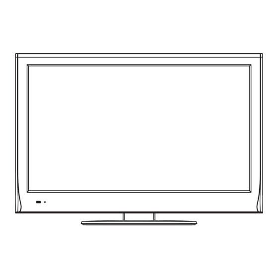
- Page 1 LCE-32R40HDW 9 82 LED-LCD TV...
-
Page 2: Table Of Contents
CONTENTS Safety precautions………………………………………………………………………..… Alignment instructions …………………………….…….………………………………… Instruction of software upgrading & boot burning ............ Working principle analysis of the unit……………………………….………….…………. Block diagram…………………………………..………………………………….………… IC block diagram………………………………………………………………………..…… Wiring diagram ……………………………………………………………………………. Troubleshooting guide ………………………………………………………………..…… Schematic diagram………………………………………………………………………… APPENDIX-A: Assembly list APPENDIX-B: Exploded View... -
Page 3: Safety Precautions
This service manual is only for service personnel to take reference with. Before Attention: servicing please read the following points carefully. Safety precautions 1. Instructions Be sure to switch off the power supply before replacing or welding any components or inserting/plugging in connection wire. - Page 4 would be unable to work and no way to get it repaired. If the connection wires, connections or components fixed by the thermotropic glue need to disengage when service, please soak the thermotropic glue into the alcohol and then pull them out in case of dagmage.
-
Page 5: Alignment Instructions
Alignment instructions 2 Adjustment equipment Digital multimeter Signal generator (54200) PC (presetting FLASH software) VG848, VG849 (VGA, YPbPr and HDMI signal generator) DVD player with HDMI output White balance apparatus (CA210) Monitor 3 Adjustment flow 3.1 Test voltage of power supply 3.1.1 According to wiring diagram "9242KC5101JL", connect main board, power board, IR board and key board correctly, switch on power supply, then press key ‘power’... - Page 6 3.2 Adjustment flow chart as Fig.1 Check if FLASH has been burned Product main board on line General assembly and adjustment White balance adjustment Connect to central signal source, check if each function of TV, such as omitted program, analog parameter control, etc. is normal? Check if output of earphones, speakers are normal? Input AV/S-VIDEO signal, check if each function of both channels are normal?
- Page 7 4 Adjustment instruction 4.1 Unit adjustment 4.1.1 According to wiring diagram ‘9242KC5101JL’ , connect main board, power board, key board and IR board correctly, switch on power supply, check if display is normal? 4.1.2 Instruction of factory menu a)First press key ‘Program source’, then press number keys “2、5、8、0” in turn to enter initial factory menu;...
- Page 8 4.2.3 White balance adjustment of YPbPr channel ADC calibration of SD mode: Input color-bar signal with format of 480i/60 Hz (VG848: Timing is 968,PAT is 918), enter into submenu “ADC adjustment” of factory menu and select item “AUTO COLOR”, system will begin calibration automatically, please note whether picture and data are abnormal clearly or not (main abnormal data phenomena are that several data are very different from the other or about 1000 more than the other);...
- Page 9 adjustment” of factory menu and select item “AUTO COLOR”, system will begin calibration automatically, Press key “Menu” to be back to upper menu, set “Program source” as VGA”, input monochrome signal with format of 800×600/60 Hz (VG848: Timing is 854,PAT is 948), enter into submenu “ADC adjustment”...
- Page 10 5 Performance check 5.1 TV port Connect RF port to central signal source, first enter into channel menu, then auto search programs, check if there is any omitted program ,output of speakers and picture are normal 5.2 AV/S-Video port Input AV/S signal to corresponding terminal respectively, check if picture and sound are normal. 5.3 YPbPr/YCbCr port Input YUV signal from signal general VG848 with YUV format listed as Table 8, check if picture and sound are normal.
- Page 11 6 User menu setting before leaving factory Enter into factory menu, select item ‘Reset’, TV set will be preset automatically before leaving factory. Be sure to do the step after completing adjustments in factory. 7 Instruction for software burning in factory as Table 10 Table 10 Instruction for software burning in factory Instruction for...
- Page 12 Instruction of software upgrade Instruction of software upgrade for KC# model: 1. Save upgrade file “flash.img” into the root directory of a U disk; 2. Insert the U disk into USB port of TV set, press key “power” until TV set is in “standby”...
- Page 13 Fig. 2 Factory menu 4. Press keys of remote control “▲”,”▼” to select item “ISP”, press key “enter” to begin updating progress, a prompt “Updating, Pls, Waiting…” is displaying, wait for a while until menu display (TV set is unable to accept other operation now), please refer to the Fig.
- Page 14 Fig. 3 Updating prompt 5. TV set will auto-reset after completing update, according to step1 and step 2, enter into factory menu again to confirm updating completion by checking the time of update file.
-
Page 15: Working Principle Analysis Of The Unit
Working principle analysis of the unit RF signal from antenna is sent into TUNER301 to be processed by HF-amplified and frequency mixing, then IF signal is outputted to SWF Z301 to be IF filtered to get ideal IF characteristics, then the signal is sent to main chip N101(RTD2674S)-27#,28# to be amplified by inline IF amplifier and synchronous demodulated to get CVBS. -
Page 16: Block Diagram
Block diagram... -
Page 17: Ic Block Diagram
IC block diagram Main IC RTD2674S Pin List VCM_BB AVDD_BB0_3.3V HDDC0_SCL AIN_5L/LSADC6 HDDC0_SDA AIO_2R HDDC1_SCL AIO_2L HDDC1_SDA AIO_1R VGA_DDC_SCL AIO_1L VGA_DDC_SDA AIN_4R IO_3.3V AIN_4L GPIO_C8 AIN_3R GPIO_C6 AIN_3L GPIO_C5 AIN_2R STBY _CORE_1.2V AIN_2L SPI_DI AIN_1R SPI_DO AIN_1L SPI_SCK AOUT_R SPI_CS_N AOUT_L RESET_IN HPOUT_R GPIO_C4... - Page 18 Main IC RTD2674S Table 1-1. RTD2674S Pin Assignments – Pin detail description (I/O Legend: A = Analog, I = Input, O = Output, P = Power, G = Ground) Pin No Pin Name Type Description Note Connect 1uF to GND VCM_BB Analog Audio Common Voltage Reference Analog 3.3V AVDD_BB0...
- Page 19 Main IC RTD2674S Digital I/O 3.3V VCC3_0 PAD I/O Power 3.3V 5V tolerance even when GPIO_A0 GPIO_A0 power-off 5V tolerance even when GPIO_A1 GPIO_A1 power-off Digital 1.2V, Power Down@ Core_1.2V Core Power 1.2V Power saving B_FP LVDS_Port_B_F_Pair_P B_FN LVDS_Port_B_F_Pair_N B_EP LVDS_Port_B_E_Pair_P B_EN LVDS_Port_B_E_Pair_N B_DP...
- Page 20 Main IC RTD2674S 5V tolerance even when GPIO_B9 GPIO_B9 power-off 5V tolerance even when GPIO_B10 GPIO_B10 power-off 5V tolerance even when GPIO_B12 GPIO_B12 power-off Digital 1.2V, Power Down@ Core_1.2V Core Power 1.2V Power saving DQS0 DDR_DQS0 DQ_7 DDR_Data7 DQ_6 DDR_Data6 SVCC25 DDR I/O Power 2.5V DQ_5 DDR_Data5...
- Page 21 Main IC RTD2674S DQ_15 DDR_Data15 DQ_14 DDR_Data14 DQ_13 DDR_Data13 DQ_12 DDR_Data12 DQ_11 DDR_Data11 DQ_10 DDR_Data10 SVCC25 DDR I/O Power 2.5V DQ_9 DDR_Data9 DQ_8 DDR_Data8 DQS1 DDR_DQS1 Digital 1.2V, Power Down@ Core_1.2V Core Power 1.2V Power saving V33_IO PAD I/O Power 3.3V Connect 10K to GND lsadc_ref LSADC reference...
- Page 22 Main IC RTD2674S 5V tolerance even when HDDC0_SDA HDMI DDC Data 0 power-off 5V tolerance even when HDDC0_SCL HDMI DDC Clock 0 power-off 5V tolerance even when HDMI CEC function power-off RX_V12 HDMI GDI Power 1.2V RX_V33 HDMI GDI Power 3.3V HDMI_1_CLKN HDMI_RX_Port1_CLK_Pair_Negative HDMI_1_CLKP...
- Page 23 Main IC RTD2674S ADC_VDC_VDD12 ADC Power 1.2V ADC_GND_OFF ADC GND VIN_11P S-Video C/Scart C Input VIN_A0N Common GND for Scart/SV VIN_9P S-Video Y/Scart Y Input VIN_12P S-Video C Input VIN_A1N Common GND for SV VIN_10P S-Video Y Input VIN_13P CVBS Input VIN_A2N Common GND for CVBS VIN_14P...
- Page 24 TAS5711 PIN ASSIGNMENT PHP Package (Top View) 48 47 46 45 44 43 42 41 40 39 38 37 OUT_A OUT_D PVDD_A PVDD_D PVDD_A PVDD_D BST_A BST_D GVDD_OUT GVDD_OUT VREG SSTIMER TAS5711 OC_ADJ AGND PBTL AVSS DVSS PLL_FLTM DVDD PLL_FLTP STEST VR_ANA RESET...
- Page 25 PIN FUNCTIONS (continued) TYPE TERMINATION DESCRIPTION TOLERANT NAME DVSS Digital ground Analog ground for power stage GVDD_OUT 5, 32 Gate drive internal regulator output. This pin must not be used to drive external devices. LRCLK Pulldown Input serial audio data left/right clock (sample rate clock) MCLK Pulldown Master clock input...
-
Page 26: Wiring Diagram
Wiring diagram... -
Page 27: Troubleshooting Guide
Troubleshooting guide 1. No raster... - Page 28 2. No picture, but sound is normal...
- Page 29 3. No sound, but picture is normal.
- Page 30 1.2V_STB 330n 53912B33K0 STBY_CORE_1.2V 3.3V_STB VADC_3.3V 3.3V_STB PLL_3.3V L101 L109 L114 BG1608B121 SGMI2012-2R2KT BG1608B121 5V_STB N102 MAX3232CSE C178 100n C179 L121 R117 SGMI3216K100KT R133 100n 003:F1 RF_AGC RF_AGC_OUT 001:C5 HDMI_1.2V VDAC_3.3V APLL_3.3V TX 002:H2 T1OUT C176 L102 L110 L115 R134 100n BG1608B121 BG1608B121...
- Page 31 HDMI1_RX2+ 001:E2 HDMI1_RX2- 001:E2 HDMI1_RX1+ 001:E2 HDMI1_RX1- 001:E2 HDMI1_RX0+ 001:E2 HDMI1_5V HDMI1_RX0- 001:E2 HDMI1_CLK+ 001:E2 R257 CM1213-08MS 001:E2 HDMI1_CLK- X208 N207 YPBPR1_Y+ 001:D2 HDMI_CEC 001:F3 JY-3541L-01-030 R258 HDMI1_SCL 001:F3 HDMI1_SDA 001:F3 VIN_Y0- 001:D2 HDMI1_5V R217 R259 BC847AW R224 RX 001:H1 4.7K YPBPR1_PB+ 001:D2...
- Page 32 L314 BG1608B121 N301 MP1484 C307 N307 L304 VCC_PANEL AO4803A SGMI3216K100KT D2_8 BC857AW COMP RF_AGC 001:E1 V314 RF_AGC D2_7 GND_4 BT_4 D1_6 D1_5 L301 R364 SLF7032T-100M1R4-PF 5V_USB C343 R327 470n TUN_SCL 001:C5 R323 R365 4.7K close to main chip V303 PANEL_ON 001:F4 BC847AW TUN_SDA...
- Page 33 AVDD2_LVDS AVDD2_LPLL VDDP2 N 4 0 1 K 4 T 5 1 1 6 3 Q G - H C F 7 AVDD2 VDDP2 005:F3 VDDP2 004:A5 M1-BA0 DQ15 B-MDATA15 004:A4 AVDD2_LVDS B-MDATA14 004:F4 B_BA1 DQ14 004:A3 AVDD2_MPLL DQ13 B-MDATA13 004:A4 VDDC_6M20S R401...
- Page 34 N601 MP1484 C642 3.3V-6M20S AVDD2_LPLL L604 BG1608B121 COMP 004:H2 AVDD2_LPLL GND_4 AVDD2_MEMPLL L610 SLF7032T-100M1R4-PF 1.26V-6M20S L605 BG1608B121 004:H1 AVDD2_MEMPLL Vout=0.923*[1+(R611+R612)/R613] OUT 1.35 v 53998010M1 2.1A AVDD2_MPLL L606 BG1608B121 004:H2 AVDD2_MPLL N602 MP1484 C649 AVDD2 L607 BG1608B121 AVDD2 004:H1 COMP GND_4 +3.3VDD AVDD2_LVDS 3.3V-6M20S...
- Page 35 R526 R527 +3.3VDD SLF12575T-220M4R0 GND-H L501 C515 2.2n GND-D C516 C508 C510 4.7n 4.7n R522 0 GND-H GND-H GND-D GND-H +3.3VDD GND-H GND-H GND-H AVDD PGND_AB_48 X502 A_SEL PGND_AB_47 GND-H R510 GND-H 001:D6 MCLK MCLK GND_49 OUT_B SLF12575T-220M4R0 OSC_RES PVDD_B_45 L504 GND-H GND-H...
- Page 37 PAD1 RESERVE POWER PAD2 GND/THD INPUT PAD3 CIN1 GPIO5 MENU 3.6K PAD8 CIN2 GPIO6 CIN3 GPIIO7 LED1 D[0] PAD4 5.6K CIN4 INT# CIN5 VOL- PAD5 LED2 D[1] CIN6 SCLK PAD6 CIN7 ADD0 LED3 D[2] CIN8 ADD1 CIN9 GPIO8 5.6K LED4 D[3] CIN10 GPIO9...
- Page 38 APPENDIX-A: Main assembly 9232KC5111-S1 LCE-32R40HDW MAIN COMPONENT AND IT'S NO. NAME 5270160001 EM6AA160TS-4G Main board XI6KC03701F0 N103 5272674001 RTD2674S N101 5272532004 W25X32VSSIG-E N104 5275711001 TAS5711 N501 Power board XI6KC0372010 Remote control XI6010J03501 RC-J35-0A Key board XI635KC02103 IR board XI635KC02201 Display panel...
- Page 39 APPENDIX-B: Exploded view (LCE-32R40HDW)
- Page 40 PART LIST OF EXPLODED VIEW REF.No. DESCRIPION Front cabinet Front cabinet decorative board IR assembly Light guided pole Panel pressing block 2 Sound box assembly Display panel Main board assembly Main board washer Power board assembly Standing pole bracket (right) Standing pole bracket (left) Power board insulated patition Interface baffle (right)
- Page 41 PART LIST LCE-32R40HDW ver. REF.No. PARTS No. DESCRIPION Q'TY REMARK XI5Q32510030 Front cabinet Front cabinet decorative board XI5850447010 XI635KC02201 IR assembly Light guided pole XI570031901A Panel pressing block 2 XI5810074600 Sound box assembly XI6170856000 Display panel XI5203328306 1 T315HW05 V0...
- Page 42 Appendix: Installing the Stand If the stand is provided, please read these instructions thoroughly before attempting this installation. You must install your TV into the stand in order for it to stand upright on a cabinet or other flat surface. If you intend to mount your TV on a wall or other vertical surface, you must remove the stand column.
- Page 44 Augest 2010...