
Related Manuals for Supermicro SUPER P6DBE


Summary of Contents for Supermicro SUPER P6DBE
- Page 1 UPER SUPER P6DBS SUPER P6DBE SUPER P6DBU SUPER P6SBU SUPER P6SBS SUPER P6SBA SUPER P6SBM USER’S AND BIOS MANUAL Revision 4.0 ®...
- Page 2 SUPERMICRO COMPUTER reserves the right to make changes to the product described in this manual at any time and without notice. This product, including software, if any, and documentation may not, in whole or in part, be copied, photocopied, reproduced, translated or reduced to any medium or machine without prior written consent.
-
Page 3: Preface
P6SBM supports Celeron and 100 MHz FSB speed Pentium III processors up to 700 MHz. (*Note: Currently, SUPER P6DBE/P6DBU/P6SBU/P6SBA motherboard supports CPU speeds up to 1GHz with 100MHz FSB speed.) Pentium III and II processors with the Dual Independent Bus Architecture are housed in a new package technology called a Single Edge Contact Cartridge (S.E.C.C.) . - Page 4 Manual UPER P6DBS/P6DBE/P6DBU/P6SBU/P6SBS/P6SBA/P6SBM If you encounter any problems, please see Chapter 3, Troubleshooting, which describes troubleshooting procedures for the video, the memory and the setup configuration stored in memory. For quick reference, a general FAQ [Frequently Asked Questions] section is provided.
-
Page 5: Table Of Contents
Overview ... 1-1 SUPER P6DBS Image ... 1-4 SUPER P6DBS Motherboard Layout ... 1-5 SUPER P6DBE Image ... 1-6 SUPER P6DBE Motherboard Layout ... 1-7 SUPER P6DBU Image ... 1-8 SUPER P6DBU Motherboard Layout ... 1-9 SUPER P6SBU Image ... 1-10 SUPER P6SBU Motherboard Layout ... - Page 6 UPER P6DBS/P6DBE/P6DBU/P6SBU/P6SBS/P6SBA/P6SBM ACPI/PC 98 Features ... 1-25 Wake-On-LAN ... 1-26 Power Supply ... 1-27 Super I/O ... 1-27 AIC 7895 SCSI Controller ... 1-28 1-10 AIC 7890 SCSI Controller ... 1-29 Chapter 2: Installation Static-Sensitive Devices ... 2-1 Precautions ... 2-1 Unpacking ...
- Page 7 DIMM Installation ... 2-13 2-10 Connecting Parallel Port, Floppy and Hard Disk Drives ... 2-14 Parallel Port Connector ... 2-15 Floppy Connector ... 2-15 IDE Connectors ... 2-15 SCSI Connectors ... 2-16 Ultra II LVD SCSI 68-pin Connector ... 2-17 AGP Port ...
-
Page 8: Jumper Quick Reference
W O L W a k e - O n - L A N *Note: SCSI jumpers and connectors do not apply to the P6DBE, P6SBA or P6SBM motherboards. P 6 D B U / P 6 S B U... -
Page 9: Front Control Panel Connector
Front Control Panel Connector Front Control Panel Connector P6DBS/DBE/DBU/SBU/ S B S / S B M IR Conn P o w e r O n R e s e t JF2 JF1 See pages 2-8 through 2-10 for pin definitions. H a r d Hard Drive Drive LED... - Page 10 Manual UPER P6DBS/P6DBE/P6DBU/P6SBU/P6SBS/P6SBA/P6SBM Notes...
-
Page 11: Chapter 1: Introduction
While all of the motherboards are the ATX form factor, the P6DBU and P6DBE have 5 PCI and 2 ISA slots with one shared. The SUPER P6DBS, P6SBU, P6SBS and P6SBA have 4 PCI and 3 ISA slots with one shared, and the SUPER P6SBM has 3 PCI and 1 ISA slots with one shared. - Page 12 Manual UPER P6DBS/P6DBE/P6DBU/P6SBU/P6SBS/P6SBA/P6SBM Included I/O on all motherboards are 2 EIDE ports, a floppy port, an ECP/EPP supported parallel port, PS/2 mouse and PS/2 keyboard ports, 2 serial ports, an infrared port and 2 USB ports. The SUPER P6DBU and P6SBU provide an onboard Adaptec 7890 Ultra II SCSI controller with data transfer rates of up to 80 MB/s and an optional RAIDport III (ARO-1130U2).
- Page 13 Chapter 1: Introduction Notes...
-
Page 14: Super P6Dbs Image
Manual UPER P6DBS/P6DBE/P6DBU/P6SBU/P6SBS/P6SBA/P6SBM SUPER P6DBS Figure 1-1. SUPER P6DBS Motherboard Image... -
Page 15: Super P6Dbs Motherboard Layout
PS/2 KB (bottom) PS/2 MOUSE (top) J17, J18 Parallel Port JP20 PCI 4 PCI 3 Chassis Intrusion PCI 2 PCI 1 JJ14 SBLINK ——–—— Manufacturer Settings —–——— J B T 1 : 1-2 (default) 2-3 CMOS Clear * To clear the CMOS completely, disconnect the power source. -
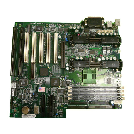
Page 16: Super P6Dbe Image
Manual UPER P6DBS/P6DBE/P6DBU/P6SBU/P6SBS/P6SBA/P6SBM SUPER P6DBE Figure 1-3. SUPER P6DBE Motherboard Image... -
Page 17: Super P6Dbe Motherboard Layout
1-2 PIIX CTL PD State 2-3 BIOS CTL PD State (default) WO L : Wake-on-LAN ——–—–——————–———–——–——–— Note: To enable the overheat buzzer, place a jumper on BZ_ON. Figure 1-4. SUPER P6DBE Motherboard Layout Chapter 1: Introduction 9.6" JP16 JP11 PIIX4E JP18 9.6"... -
Page 18: Super P6Dbu Image
Manual UPER P6DBS/P6DBE/P6DBU/P6SBU/P6SBS/P6SBA/P6SBM SUPER P6DBU Figure 1-5. SUPER P6DBU Motherboard Image... -
Page 19: Super P6Dbu Motherboard Layout
PS/2 KB (bottom) PS/2 MOUSE (top) J17, J18 Parallel Port JP20 PCI 5 PCI 4 Chassis Intrusion PCI 3 PCI 2 SBLINK PCI 1 ——–—— Manufacturer Settings —–——— J B T 1 : 1-2 (default) 2-3 CMOS Clear * To clear the CMOS completely, disconnect the power source. -
Page 20: Super P6Sbu Image
Manual UPER P6DBS/P6DBE/P6DBU/P6SBU/P6SBS/P6SBA/P6SBM SUPER P6SBU Figure 1-7. SUPER P6SBU Motherboard Image 1-10... -
Page 21: Super P6Sbu Motherboard Layout
PS/2 KB (bottom) PS/2 MOUSE (top) J17, J18 JOH: Overheat LED Parallel Port 12" 1938 JPSI JJ14 JTM1 ——–—— Manufacturer Settings —–——— J B T 1 : 1-2 (default) 2-3 CMOS Clear To clear the CMOS completely, disconnect the power source. J L 1 : OFF (default) ON (intrusion) -
Page 22: Super P6Sbs Image
Manual UPER P6DBS/P6DBE/P6DBU/P6SBU/P6SBS/P6SBA/P6SBM SUPER P6SBS Figure 1-9. SUPER P6SBS Motherboard Image 1-12... -
Page 23: Super P6Sbs Motherboard Layout
PS/2 KB (bottom) PS/2 MOUSE (top) J17, J18 JOH: Overheat LED JA5, JA6: SCSI Termination Parallel Port Chassis 12" Intrusion SBLINK JJ14 ——–—— Manufacturer Settings —–——— J B T 1 : 1-2 (default) 2-3 CMOS Clear To clear the CMOS completely, disconnect the power source. -
Page 24: Super P6Sba Image
Manual UPER P6DBS/P6DBE/P6DBU/P6SBU/P6SBS/P6SBA/P6SBM SUPER P6SBA Figure 1-11. SUPER P6SBA Motherboard Image 1-14... -
Page 25: Super P6Sba Motherboard Layout
PS/2 KB (bottom) PS/2 MOUSE (top) J17, J18 Parallel Port 12" JP20 BIOS ——–—— Manufacturer Settings —–——— J B T 1 : 1-2 (default) 2-3 CMOS Clear To clear the CMOS completely, disconnect the power source. J L 1 : OFF (default) ON (intrusion) J P 1 1 :... -
Page 26: Super P6Sbm Image
Manual UPER P6DBS/P6DBE/P6DBU/P6SBU/P6SBS/P6SBA/P6SBM SUPER P6SBM Figure 1-13. SUPER P6SBM Motherboard Image 1-16... -
Page 27: Super P6Sbm Motherboard Layout
PS/2 KB (bottom) PS/2 MOUSE (top) J17, J18 Parallel Port LINE LINE 9.6" MONO JP20 AUDIO 1938 JJ14 ——–—— Manufacturer Settings —–——— J B T 1 : 1-2 (default) 2-3 Clear CMOS To clear CMOS completely, disconnect the power source. J L 1 : OFF (default) ON (intrusion) -
Page 28: 440Bx Agp Chipset: System Block Diagram
Manual UPER P6DBS/P6DBE/P6DBU/P6SBU/P6SBS/P6SBA/P6SBM C P U C P U Host Bus S D R A M A G P 440BX Port PCI Slots SMBus APIC PIIX4E IDE Ports Power SCSI Management U S B U S B Ports ISA Slots BIOS Figure 1-15. - Page 29 100 MHz bus speed a single processor only.) (Also see note on processors - page 2-3.) (*Note: Currently, the P6DBE/P6DBU/P6SBU/P6SBA motherboard supports CPU speeds up to 1GHz with 100 MHz FSB speed.) M e m o r y •...
- Page 30 UPER P6DBS/P6DBE/P6DBU/P6SBU/P6SBS/P6SBA/P6SBM • System resource alert • Hardware BIOS virus protection • Auto-switching voltage regulator for the CPU core • SUPERMICRO Super Doctor and (optional) Intel Manager (LDCM) support ACPI/PC 98 Features • Microsoft OnNow • Slow blinking LED for suspend state indicator •...
-
Page 31: Chipset Overview
Dimensions • SUPER P6DBS - ATX (12" x 9.65") • SUPER P6DBE - ATX (12" x 9.6") • SUPER P6DBU - ATX (12" x 9.65") • SUPER P6SBU - ATX (12" x 8.875") • SUPER P6SBS - ATX (12" x 8.875") •... - Page 32 CPU is in sleep mode. When in sleep mode, the CPU will not run at full power, thereby generating less heat. the user has the option to shut down the CPU fan. CPU Overheat Alarm, LED and Control in P6DBS/P6DBE/ P6DBU/P6SBU/P6SBS/P6SBM This feature is available when the user enables the CPU overheat warning function in the BIOS (see page 5-18).
- Page 33 The system BIOS is protected by hardware so that no virus can infect the BIOS area. The user can only change the BIOS content through the flash utility provided by SUPERMICRO. infecting the BIOS area and destroying valuable data. Auto-Switching Voltage Regulator for the CPU Core The switching voltage regulator for the CPU core can support up to 20A current, with the auto-sensing voltage ID ranging from 1.4V to 3.5V.
-
Page 34: Solo-1 Pci Audio Drive
UPER P6DBS/P6DBE/P6DBU/P6SBU/P6SBS/P6SBA/P6SBM Solo-1 PCI Audio Drive (Standard on P6SBM, OEM option on P6SBU) The Solo-1 PCI Audio Drive feature implements a single-chip PCI audio solu- tion to provide high quality audio processing while maintaining full legacy DOS game compatibility. With a dynamic range of over 80 dB, the Solo-1 complies with the Microsoft PC 97/PC 98 specifications and meets WHQL audio requirements. -
Page 35: Acpi/Pc 98 Features
ACPI/PC 98 Features ACPI stands for Advanced Configuration and Power Interface. specification defines a flexible and abstract hardware interface that pro- vides a standard way to integrate power management features throughout a PC system, including hardware, operating system and application soft- ware. -
Page 36: Wake-On-Lan
UPER P6DBS/P6DBE/P6DBU/P6SBU/P6SBS/P6SBA/P6SBM Real Time Clock Wake-Up Alarm Although the PC may be perceived to be off when not in use, it is still capable of responding to preset wake-up events. In the BIOS, the user can set a timer to wake-up the system at a predetermined time (see page 5-15). -
Page 37: Power Supply
It is even more important for Pentium II and III processors that have high CPU clock rates of 300 MHz and above. The SUPER P6DBS/P6DBE/P6DBU/P6SBU/P6SBS/P6SBA/P6SBM accommo- dates ATX power supplies. the specifications required by the CPU, some are inadequate. - Page 38 UPER P6DBS/P6DBE/P6DBU/P6SBU/P6SBS/P6SBA/P6SBM The Super I/O provides functions that comply with ACPI (Advanced Con- figuration and Power Interface), which includes support of legacy and ACPI power management through an SMI or SCI function pin. auto power management to reduce power consumption.
- Page 39 Chapter 1: Introduction 1-10 AIC-7890 Ultra II SCSI Note: If you are using a low voltage differential hard drive, it is recommended that you use an LVD/SE Ultra II SCSI cable. LVD/SE cables offer increased length and can accommodate more devices. The SUPER P6DBU/P6SBU has an onboard SCSI controller that is 100% compatible with all major operating and hardware platforms.
- Page 40 Manual UPER P6DBS/P6DBE/P6DBU/P6SBU/P6SBS/P6SBA/P6SBM Notes 1-30...
-
Page 41: Chapter 2: Installation
• Handle the board by its edges only; do not touch its components, peripheral chips, memory modules or gold contacts. • When handling chips or modules, avoid touching their pins. • Put the system board and peripherals back into their antistatic bags when not in use. - Page 42 Manual UPER P6DBS/P6DBE/P6DBU/P6SBU/P6SBS/P6SBA/P6SBM 2. Install the retention mechanism attach mount under the motherboard. Do this before mounting the motherboard in the chassis. Do not screw it in too tight. Mount the two black plastic pegs onto the motherboard (Figure 2-1).
- Page 43 Chapter 2: Installation alignment notch in the SECC cartridge fits over the plug in Slot 1. Push the processor down firmly, with even pressure on both sides of the top, until it is seated. Figure 2-2. Retention Mechanism Top of Processor Heat Sink Do not screw in too tight! 6.
- Page 44 UPER P6DBS/P6DBE/P6DBU/P6SBU/P6SBS/P6SBA/P6SBM 7. Attach the small end of the power cable (C in Figure 2-3) to the three-pin connector on the processor, then attach the large end to the three-pin connector on the motherboard. Figure 2-3. Attaching the Fan Power Cable When removing the Pentium III/II processor, avoid press- ing down on the motherboard or components.
-
Page 45: Installation Of The Universal Retention Mechanism
Installation of the Universal Retention Mechanism (URM)* Please Note! Screws and washers attach from the bottom of the board and must be installed before mounting the board to the chassis. (See Figures 2-4 and 2-5.) 1. When installing the URM, be sure the Left (L) and Right (R) sides are placed accordingly.** 2. - Page 46 Manual UPER P6DBS/P6DBE/P6DBU/P6SBU/P6SBS/P6SBA/P6SBM Figure 2-4. Installing a Celeron Processor Figure 2-5. URM and Celeron Installation Supero Screw holes for retention URM with arms folded mechanism Note: Left and Right arms are defined Note notch in socket Top view of Celeron cap...
-
Page 47: Explanation And Diagram Of Jumper/Connector
Explanation and Diagram of Jumper/ Connector To modify the operation of the motherboard, jumpers can be used to choose between optional set- tings. Jumpers create shorts be- tween two pins to change the function of the connector. Pin 1 is identified with a square. -
Page 48: Mounting The Motherboard In The Chassis
UPER P6DBS/P6DBE/P6DBU/P6SBU/P6SBS/P6SBA/P6SBM Mounting the Motherboard in the Chassis All the motherboards have standard mounting holes to fit different types of chas- sis. Chassis may come with a variety of mounting fasteners made of metal or plastic. Although a chassis may have both metal and plastic fasteners, metal fasteners are the most highly recommended because they ground the system board to the chassis. -
Page 49: Pw_On Connector
PW_ON Connector The PW_ON connector is located on pins 9 and 10 of JF2. Momentarily contacting both pins will power on/off the system. The user can also con- figure this button to function as a suspend button. (See the Power Button Function in BIOS on page 5- 13.) To turn off the power when set to suspend mode, hold down the... -
Page 50: Speaker Connector
UPER P6DBS/P6DBE/P6DBU/P6SBU/P6SBS/P6SBA/P6SBM Speaker Connector The speaker connector is located on pins 10 to 13 of JF1. See Table 2-9 for pin definitions. Power Save State Select Refer to Table 2-10 to set JP20. The Power Save State Select is used... -
Page 51: Cmo Clear
ATX Serial Ports ATX serial port COM1 is located on J20 and serial port COM2 is located on J21. See Table 2-13 for pin definitions. CMOS Clear Refer to Table 2-14 for instructions on how to clear CMOS. For an ATX power supply, you must com- pletely shut down the system, then use JBT1 to clear CMOS. -
Page 52: Chassis Intrusion
UPER P6DBS/P6DBE/P6DBU/P6SBU/P6SBS/P6SBA/P6SBM Chassis Intrusion The Chassis Intrusion Detector is located on JL1. See the board lay- outs in Chapter 1 and the PC Health Monitor section (page 1-22) for more information. See Table 2-18 for pin definitions. PCI Audio Drive Connectors (P6SBM, OEM option on P6SBU) Boards with PCI Audio Drive have additional input jacks and connectors installed. -
Page 53: Installing Dimms
Installing DIMMs Exercise extreme care when installing or removing the DIMM modules to prevent any possible damage. DIMM Installation (See Figure 2-6) 1. Insert DIMMs in Bank 0 through Bank 3 as required for the desired system memory. 2. Insert each DIMM module vertically into its slot. Pay attention to the two notches along the bottom of the module to prevent inserting the DIMM incorrectly. -
Page 54: Connecting Parallel Port, Floppy And Hard Disk Drives
UPER P6DBS/P6DBE/P6DBU/P6SBU/P6SBS/P6SBA/P6SBM 2-10 Connecting Parallel Port, Floppy and Hard Disk Drives Use the following information to connect the floppy and hard disk drive cables. • The floppy disk drive cable has seven twisted wires. • A red mark on a wire typically designates the location of pin 1. -
Page 55: Parallel Port Connector
Table 2-21 Parallel Port Pin Definitions for Connector J19 Pin Number Function Pin Number Strobe- Data Bit 0 Data Bit 1 Data Bit 2 Data Bit 3 Data Bit 4 Data Bit 5 Data Bit 6 Data Bit 7 A C K B U S Y S L C T Floppy Connector... -
Page 56: Scsi Connectors
UPER P6DBS/P6DBE/P6DBU/P6SBU/P6SBS/P6SBA/P6SBM SCSI Connectors There are no jumpers to configure the onboard Single End SCSI inter- face. Refer to Table 2-24 for pin defi- nitions. Refer to Table 2-25 for the Wide SCSI pin definitions. 50-pin Wide SCSI Connector Pin Definitions... -
Page 57: Ultra Ii Lvd Scsi 68-Pin Connector
Table 2-26 68-pin Ultra II LVD SCSI Connector Connector Contact N u m b e r Signal Names +DB(12) +DB(13) +DB(14) +DB(15) +DB(P1) +DB(0) +DB(1) +DB(2) +DB(3) +DB(4) +DB(5) +DB(6) +DB(7) +DB(P) G R O U N D D I F F S E N S T E R M P W R T E R M P W R R E S E R V E D... -
Page 58: Agp Port
UPER P6DBS/P6DBE/P6DBU/P6SBU/P6SBS/P6SBA/P6SBM Pin # Table 2-27 AGP Port Pin Definitions for J8 Pin # Spare 1 2 V Vddq3.3 5.0V Spare A D 2 1 5.0V Reserved* A D 1 9 U S B + U S B - G N D... -
Page 59: Troubleshooting Flowchart
Troubleshooting Procedures Use the following procedures and flowchart to troubleshoot your system. If you have followed all of the procedures below and still need assistance, refer to the ‘Technical Support Procedures’ and/or ‘Returning Merchandise for Service’ section(s) in this chapter. Before Power On 1. -
Page 60: No Power
UPER P6DBS/P6DBE/P6DBU/P6SBU/P6SBS/P6SBA/P6SBM No Power 1. Make sure that the default jumper is on and the CPU is correctly set 2. Check the power supply voltage monitor. (Check the power supply 115V/230V switch.) 3. If the power is still not on, turn off the system power and move the jumper setting on JP20 from 2-3 to 1-2. -
Page 61: Losing The System's Setup Configuration
Question' (FAQ) sections in this chapter of the manual or see our web site FAQs (http://www.supermicro.com/TechSupport.htm) before contact- ing Technical Support. 2. Take note that as a motherboard manufacturer, SUPERMICRO does not sell directly to end-users, so it is best to check with your distributor or reseller for troubleshooting services. -
Page 62: Frequently Asked Questions
5. The user should populate the DIMMs starting with the DIMM slot located farthest from the BX chip (U2 on P6DBS/P6DBE/P6SBS, U4 on P6DBU/ P6SBU or U9 on P6SBA). 6. If EDO memory is used, the CPU bus should be set to 66 MHz only. - Page 63 I have memory problems. to use and which BIOS setting should I choose? Answer: The correct memory to use on the SUPER P6DBS/P6DBE/P6DBU/ P6SBU/P6SBS/P6SBA is 168-pin DIMM 3.3v non-buffered SPD (Serial Present Detection) SDRAM, SDRAM and EDO memory. SPD SDRAM is preferred but is not necessary.
- Page 64 Manual UPER P6DBS/P6DBE/P6DBU/P6SBU/P6SBS/P6SBA/P6SBM Question: Which Operating System (OS) supports AGP? Answer: At present, Windows 98 and Windows NT 5.0 are the only OS that have built-in support for AGP. Some AGP video adapters can run Windows 95 OSR2.1 with special drivers.
- Page 65 Question: How do I install the sound driver for the built-in ES1938 AudioDrive? Answer: Insert the Supermicro CD that came with the motherboard into your CD- ROM drive. Double click on your CD-ROM icon (which can be found in "My Computer") to access the CD, then double click on the red "S"...
-
Page 66: Returning Merchandise For Service
UPER P6DBS/P6DBE/P6DBU/P6SBU/P6SBS/P6SBA/P6SBM Question: Do I need to change any settings to use a single proces- sor on a dual processor board? Answer: There are no jumpers or BIOS settings that need to be changed when running a single CPU on a dual processor board. In addition, you can use a single processor in either CPU slot. -
Page 67: Chapter 4: Amibios
Introduction This chapter describes the AMIBIOS for the Intel 440BX Pentium II 233/266/ 300/333/350/400/450 MHz and Pentium III MHz processors. The AMI ROM BIOS is stored in the Flash EEPROM and can be easily upgraded using a floppy disk-based program. System BIOS The BIOS is the Basic Input Output System used in all IBM ®... -
Page 68: Bios Features
BIOS Manual American AMIBIOS (c) 1997 American Megatrends, Inc. M e g a Trends 0404981500 Pentium II Motherboard Made in USA R1.0 U P E R BIOS date code Checking NVRAM xxxxx KB OK Hit <DEL> if you want to run SETUP (C) Super Micro Computer, Inc., XX-XXXX-XXXXXX-XXXXXXXX-XXXXXX-XXXX-X BIOS Features... -
Page 69: Bios Configuration Summary Screen
• Five positive voltage inputs • Two negative voltage inputs • Three fan-speed monitor inputs BIOS Configuration Summary Screen AMIBIOS displays a screen that looks similar to the following when the POST routines complete successfully. AMIBIOS System Configuration (C) 1985-1997 American Megatrends Inc., Main Processor : Pentium(tm) II Math Processor... - Page 70 BIOS Manual Figure 4-1. Standard Option Highlighted Figure 4-2. Settings for Standard Setup...
-
Page 71: Chapter 5: Running Setup
*Optimal and Fail-Safe default settings are bolded in text unless otherwise noted. The WinBIOS Setup options described in this section are selected by choosing the appropriate high-level icon from the Standard Setup screen. All displayed icons are described in this section, although the screen display is often all you need to understand how to set the options. - Page 72 BIOS Manual Entering Drive Parameters You can also enter the hard disk drive parameters. The drive parameters are: Parameter Description Type The number for a drive with certain identification parameters. Cylinders The number of cylinders in the disk drive. H e a d s The number of heads.
-
Page 73: Advanced Setup
Date and Time Configuration Select the Standard option. Select the Date/Time icon. The current values for each category are displayed. Enter new values through the keyboard. Floppy A Floppy B Choose the Floppy Drive A or B icon to specify the floppy drive type. The settings are Not Installed, 360 KB 5¼... - Page 74 BIOS Manual Pri Master ARMD Emulated as Pri Slave ARMD Emulated as Sec Master ARMD Emulated as Sec Slave ARMD Emulated as Options for Pri Master ARMD Emulated as, Pri Slave ARMD Emulated as, Sec Master ARMD Emulated as and Sec Slave ARMD Emulated as are Auto, Floppy or Hard disk .
- Page 75 Chapter 5: Running Setup booting). If selected as No and all selected boot devices failed to boot, the BIOS will try not to boot from the other boot devices which may be present but not selected as boot devices in setup. Initial Display Mode This option determines the display screen with which the POST is going to start the display.
- Page 76 BIOS Manual Primary Display This option specifies the type of display adapter card installed in the system. The settings are Absent, VGA/EGA , CGA40x25 , CGA80x25 or Mono . Password Check This option enables the password check option every time the system boots or the end user runs WinBIOS Setup.
-
Page 77: Chipset Setup
Chapter 5: Running Setup MPS Revision The settings for this option are 1.1 or 1.4. C000, 16K Shadow C400, 16K Shadow These options specify how the 32 KB of video ROM at C0000h is treated. The settings are: Disabled , Enabled or Cached . When set to Disabled, the contents of the video ROM are not copied to RAM. - Page 78 BIOS Manual - In an ECC configuration, the 82443BX asserts SERR#, for single bit (correctable) ECC errors or multiple bit (non-correctable) ECC errors if SERR# signaling is enabled via the ERRCMD control register. Any ECC errors received during initialization should be ignored. - The 82443BX asserts SERR# for one clock when it detects a target abort during 82443BX initiated PCI cycle - The 82443BX can also assert SERR# when a PCI parity error occurs during the address or data phase...
- Page 79 Multi-Trans Timer (Clks) This option specifies the multi-trans latency timings (in PCI clocks) for devices in the computer. It reduces overhead switching between different masters. The settings are Disabled , 32 , 64 , 96 , 128 , 160 , 192 or 224 . PCI1 to PCI0 Access PCI1 refers to AGP in BX and LX chipsets.
- Page 80 BIOS Manual DRAM Refresh Rate This option specifies the interval between Refresh signals to DRAM system memory. The settings for this option are 15.6 us (micro-sec- onds), 31.2 us , 62.4 us , 124.8 us or 249.6 us . Memory Hole This option specifies the location of an area of memory that cannot be addressed on the ISA bus.
- Page 81 Chapter 5: Running Setup ACPI Control Register The settings for this option are Enabled or Disabled . Set this option to Enabled to enable the ACPI (Advanced Configuration and Power Interface) control register. Gated Clock Signal GCLKEN enables internal dynamic clock gating in the 82443BX when a AGPset "IDLE"...
- Page 82 BIOS Manual 8bit I/O Recovery Time This option specifies the length of a delay inserted between consecutive 8-bit I/O operations. The settings are Disabled , 1 SYSCLK , 2 SYSCLKs , 3 SYSCLKs , 4 SYSCLKs , 5 SYSCLKs , 6 SYSCLKs , 7 SYSCLKs or 8 SYSCLKs .
-
Page 83: Power Management
Chapter 5: Running Setup DMA6 Type DMA7 Type These options specify the bus that the specified DMA channel can be used on. The settings are PC/PCI , Distributed , or Normal ISA . Memory Buffer Strength The settings for this option are Strong or Auto . Manufacturer's Setting Note: The user should always set this option to Mode 0. - Page 84 BIOS Manual Hard Disk Power Down Mode This option specifies the power conserving state that the hard disk drive enters after the specified period of hard drive inactivity has expired. The settings are Disabled , Standby , or Suspend . Note: The Optimal default setting for this option is Suspend and the Fail-Safe default setting is Disabled .
-
Page 85: Pci/Pnp Setup
Chapter 5: Running Setup display activity for the length of time specified in the Standby Timeout (Minute) option, the computer enters a power savings state. The settings are Monitor or Ignore . Device 6 (Serial port 1) Device 7 (Serial port 2) Device 8 (Parallel port) Device 5 (Floppy disk) Device 0 (Primary Master IDE) - Page 86 BIOS Manual PCI VGA Palette Snoop The settings for this option are Disabled or Enabled. When set to Enabled, multiple VGA devices operating on different buses can handle data from the CPU on each set of palette registers on every video device. Bit 5 of the command register in the PCI device configuration space is the VGA Palette Snoop bit (0 is disabled).
- Page 87 Chapter 5: Running Setup PCI Slot1 IRQ Priority PCI Slot2 IRQ Priority PCI Slot3 IRQ Priority PCI Slot4 IRQ Priority These options specify the IRQ priority for PCI devices installed in the PCI expansion slots. The settings are Auto, (IRQ) 3, 4, 5, 7, 9, 10, or 11, in priority order .
-
Page 88: Peripheral Setup
BIOS Manual Reserved Memory Size This option specifies the size of the memory area reserved for legacy ISA adapter cards. The settings are Disabled , 16K , 32K or 64K . Reserved Memory Address This option specifies the beginning address (in hex) of the reserved memory area. - Page 89 Chapter 5: Running Setup H/W Monitor In6 (-5V) CPU1 Fan CPU2 Fan Thermal Control Fan The above features are for PC Health Monitoring. The motherboards with W83781D have seven on-board voltage monitors for the CPU core, CPU I/O, +3.3V, +5V, -5V, +12V, and -12V, and three fan status monitors. Power Loss Control This option determines how the system will respond when power is lost and then comes back.
-
Page 90: Security Setup
BIOS Manual Parallel Port Mode This option specifies the parallel port mode. The settings are Normal , Bi-Dir , EPP or ECP . When set to Normal, the normal parallel port mode is used. Use Bi-Dir to support bidirectional transfers. Use EPP (Enhanced Parallel Port) to provide asymmetric bidirectional data transfer driven by the host device. -
Page 91: Fail-Safe Defaults
When you select Supervisor or User, AMIBIOS prompts for a password. You must set the Supervisor password before you can set the User password. Enter a 1-6 character password. appear on the screen when typed. prompted and press <Enter>. Make sure you write it down. If you forget it, you must drain CMOS RAM and reconfigure. - Page 92 BIOS Manual Notes 5-22...
- Page 93 Appendix A: BIOS Error Beep Codes Appendix A BIOS Error Beep Codes & Messages During the POST (Power-On Self-Test) routines, which are performed each time the system is powered on, errors may occur. Non-fatal errors are those which, in most cases, allow the system to continue the boot-up process.
- Page 94 BIOS User’s Manual Beeps Error message Refresh Failure Parity Error Base 64 KB Memory Failure Timer Not Operational Processor Error 8042 - Gate A20 Failure Processor Exception Interrupt Error Display Memory Read/Write Error ROM Checksum Error CMOS Shutdown Register Read/Write Error Refer to the table on page A-3 for solutions to the error beep codes.
-
Page 95: Appendix A: Bios Error Beep Codes
If it beeps... 1, 2, 3 times 6 times 8 times 9 times 4, 5, 7, or 10 times Appendix A: BIOS Error Beep Codes then ... reseat the DIMM memory. system still beeps, replace the memory. reseat the keyboard controller chip. If it still beeps, replace the keyboard controller. - Page 96 BIOS User’s Manual Error Message 8042 Gate -- A20 Error Address Line Short! C: Drive Error C: Drive Failure Cache Memory Bad CH-2 Timer Error CMOS Battery State Low CMOS Checksum Failure CMOS System Option Not Set CMOS Display Type Mismatch CMOS Memory Size Mismatch...
- Page 97 Error Message CMOS Time and Date Not Set D: Drive Error D: Drive Failure Diskette Boot Failure Display Switch Not Proper DMA Error DMA #1 Error DMA #2 Error FDD Controller Failure HDD Controller Failure INTR #1 Error INTR #2 Error Appendix A: BIOS Error Beep Codes Information Run Standard Setup to set the date and time...
- Page 98 BIOS User’s Manual Error Message Invalid Boot Diskette Keyboard Is Locked... Unlock It Keyboard Error KB/Interface Error No ROM BASIC Off Board Parity Error On Board Parity Error Parity Error???? Information The BIOS can read the disk in floppy drive A:, but cannot boot the computer.
- Page 99 Appendix B: AMIBIOS POST Diagnostics Error Messages AMIBIOS POST Diagnostic Error This section describes the power-on self-tests (POST) port 80 codes for the AMIBIOS. Check Point Description Code copying to specific areas is done. to INT 19h boot loader next. NMI is Disabled.
- Page 100 BIOS User’s Manual Check Point Description The keyboard controller command byte is written. Next, issuing the pin 23 and 24 blocking and unblocking commands. Next, checking if the <End or <Ins> keys were pressed during Initialize CMOS RAM in every boot AMIBIOS POST option was set in AMIBCP or the <End>...
-
Page 101: Appendix B: Amibios Post Diagnostics Error Messages
Appendix B: AMIBIOS POST Diagnostics Error Messages Check Point Description Initialization before setting the video mode is complete. Configuring the monochrome mode and color mode settings next. Bus initialization system, static, output devices will be done next, if present. Passing control to the video ROM to perform any required configuration before the video ROM test. - Page 102 BIOS User’s Manual Check Point Description Initializing the bus input, IPL, and general devices next, if present. Displaying bus initialization error messages. The new cursor position has been read and saved. Displaying the Hit <DEL> message next. Preparing the descriptor tables next. The descriptor tables are prepared.
- Page 103 Appendix B: AMIBIOS POST Diagnostics Error Messages Check Point Description The memory below 1 MB has been cleared via a soft reset. Clearing the memory above 1 MB next. The memory above 1 MB has been cleared via a soft reset.
- Page 104 BIOS User’s Manual Check Point Description The DMA page register test passed. DMA Controller 1 base register test next. The DMA controller 1 base register test passed. Performing the DMA controller 2 base register test next. The DMA controller 2 base register test passed. Programming DMA controllers 1 and 2 next.
- Page 105 Appendix B: AMIBIOS POST Diagnostics Error Messages Check Point Description programming been completed. Uncompressing the WINBIOS Setup code and executing the AMIBIOS Setup or WINBIOS Setup utility next. Returned from WINBIOS Setup and cleared the screen. Performing any necessary programming after WINBIOS Setup next.
- Page 106 BIOS User’s Manual Check Point Description Any initialization required after the option ROM test has been completed. printer base address next. Set the timer and printer base addresses. RS-232 base address next. Returned Performing Coprocessor test next. Required initialization before the Coprocessor test is over.
- Page 107 Appendix B: AMIBIOS POST Diagnostics Error Messages Check Point Description Returned Next, performing the E000 option ROM had control. Initialization completed. Displaying the system configuration next. Building the multiprocessor table, if necessary. POST next. The system configuration is displayed. Uncompressing the DMI data and initializing DMI. Copying any code to specific areas.
- Page 108 BIOS User’s Manual If either <Ctrl><Home>was pressed or the system BIOS checksum is bad, next the system will go to checkpoint code E0h. Otherwise, going to checkpoint code D7h. B-10...
Need help?
Do you have a question about the SUPER P6DBE and is the answer not in the manual?
Questions and answers